Special Counter/dividers
The last two chapters looked at D-type and JK flip-flops and showed how they are used in various ‘up’-counting counter/divider ICs. The present chapter rounds off this subject by looking at some of the special types of digital counter/divider ICs that are available, including ‘presettable’ and ‘down’- and ‘up/down’- counting types.
Directional Control
Chapter 10 explained how D-type and JK flip-flops work and described how a D-type can be made to act as a binary divider (divide-by-2) stage by connecting its D and NOT-Q terminals together as shown in Figure 12.1(a), and a JK-type can be made to act in the same way by tying its J and K terminals to logic-1 as shown in Figure 12.1(b). Note from the symbols of these diagrams that the D-type’s actions are triggered by the rising edges of the clock signals, and the JK’s are triggered by falling edges.
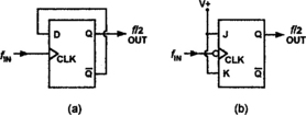
Figure 12.1 General circuit diagram of (a) D-type and (b) JK divide-by-2 stages; the D-type uses rising-edge triggering; the JK is falling-edge triggered
Figure 12.2 shows how D-type or JK divider stages can be cascaded to make ripple-mode binary counters in which the output of the first stage is used to clock the input of the second stage, and so on for however many stages there are. In rising-edge triggered D-type circuits the clock pulses are taken from NOT-Q outputs, as shown in (a), but in falling-edge triggered JK circuits they are taken from Q outputs, as in (b). Both circuits have the same Q-output Truth Table, which for a 2-stage ripple counter is as shown in (c); if you compare this Table with that of Figure 11.1 (in Chapter 11) you’ll notice that the 4-step sequential binary coded outputs of Figure 12.2 correspond with normal Decimal (BCD) coding, and run 0–1–2–3–0–, etc as the clock goes through cycles 0–1–2–3–0–, etc.
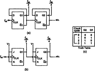
Thus, the Figure 12.2 type of counter gives a sequentially upwards-counting clocking cycle, which repeatedly runs from 0 to 3 in a 2-bit counter, or 0 to 7 in a 3-bit counter, and so on. Consequently, all circuits of this basic type are known as ‘up’ counters, irrespective of their bit count or whether they give a synchronous or asynchronous type of clocking action, etc.
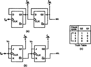
The counting action of a ripple counter can be reversed, so that it counts downwards rather than upwards, by using the basic connections shown in Figure 12.3, in which the clocking output of each stage is taken from the complement of that used in Figure 12.2 (i.e. from Q rather than NOT-Q, or vice versa). A 2-bit counter of this type generates the Truth Table shown in Figure 12.3(c), in which the sequential BCD coding runs 3–2–1–0–3–, etc. as the clock goes through cycles 0–1–2–3–0–, etc. This type of counter gives a sequentially downwards-counting clocking cycle, which repeatedly runs from 3 to 0 in a 2-bit counter, or 7 to 0 in a 3-bit counter, and so on. Consequently, all circuits of this basic type are known as ‘down’ counters, irrespective of their bit count or whether they give a synchronous or asynchronous type of clocking action, etc.
A ripple counter can be configured to count in either direction by fitting it with gate-controlled clock-source options, as shown in the JK example of Figure 12.4. Here, when the COUNT-UP line is biased to logic-1 and the COUNT-DOWN line is biased to logic-0 the G1 and G4 AND gates are enabled and pass ‘Q’ clock signals to FF2 and FF3 (etc.), but gates G2 and G5 are disabled and block the NOT-Q signals; the circuit thus acts like that of Figure 9.2(b) under this condition, and gives an up-counting action. But when the COUNT-DOWN line is biased to logic-1 and COUNT-UP is at logic-0 the G1 and G4 gates are disabled and G2 and G5 are enabled and pass NOT-Q clock signals, and under this condition the circuit acts like that of Figure 12.3(b) and gives a down-counting action. All circuits of this basic type are known as ‘up/down’ counters, irrespective of their bit count or their precise form of construction, etc.
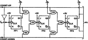
The Figure 12.4 up/down circuit uses individual COUNT-UP and COUNT-DOWN control lines, which must always by connected in opposite logic states. The circuit can be modified for control via a single UP/DOWN input terminal by wiring an inverter between the two lines, as shown dotted in the diagram, so that the circuit gives ‘up’ counting when the upper line is biased to logic-1, and ‘down’ counting when it is biased to logic-0. Some up/down counters use two clock lines, one for up counting and the other for down counting; these counters are internally similar to Figure 12.4 but have the clock and direction-control lines effectively combined via logic networks that control the clock feed to FF1 as well as all the other flip-flop stages.
Thus, the electronics engineer has many options when designing modern counter/divider circuits. The usual option is to use a conventional synchronous or asynchronous up-counting IC, and most of the finer points of this subject are covered in Chapter 11. There are also the options of using ‘down’ or ‘up/down’ counters; both of these options are dealt with later in the present chapter, but first it is necessary to look at yet another option, that of using ‘programmable’ counter/divider ICs.
‘Programmable’ Counter Basics
Many ‘counter’ ICs can be used in both counting and dividing applications, and are thus known as counter/divider ICs. Figure 12.5, for example, shows how two ordinary BCD divide-by-10 stages can be used as a divide-by-100 circuit that (a) gives a stable output frequency of 1kHz if fed with a stable 100kHz clock signal, or (b) produces 27 output pulses (cycles) when clocked via 2700 randomly timed input pulses. Note that neither of these circuits gives any visual output information (via 7-segment displays, etc.).
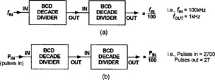
Figure 12.6 shows, in block diagram form, how the Figure 12.5(b) pulse cycle divider circuit can be converted into a pulse counter by simply fitting it with digital readout circuitry, so that the user can actually see the results of the divide-by-100 action. Thus the basic difference between a counter and a divider is one of usage; a counter usually has a visual readout, and a divider has not.
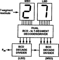
Figure 12.6 The Figure 12.5(b) pulse-count divider can be used as a pulse counter by fitting it with a digital readout facility
Most conventional ‘up’ counters have a RESET facility that enables all Q outputs to be set to zero at any time, thus giving a BCD ‘0’ output. This facility is – as already described – also useful in enabling the counter’s divide-by figure to be preset to any desired value, N, by connecting the outputs back to the RESET terminal so that the outputs reset to the BCD ‘0’ state on the arrival of every Nth clock pulse, but a weakness here is that the IC has to be hard-wired to give a specific divide-by figure, and this sometimes involves the use of external gating circuitry, etc. One way around this snag is to provide the IC with an additional PROGRAMMING control that enables its outputs to be set to any desired binary values when the control is activated.
Figure 12.7 illustrates the basic idea behind the programmable counter. Here, any desired 4-bit binary code can be applied to the IC’s four ‘P’ terminals, and the IC’s 4-bit output is forced to agree with this code whenever the PRESET control is activated. In practice, this type of IC may be known as a ‘programmable’ or ‘presettable’ counter, its input facilities may be named PRESET or
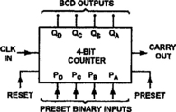
Figure 12.7 The Q outputs of a programmable counter can be forced into preset binary states via a PRESET control
PARALLEL LOAD or JAM controls, and the controls may be activated by a logic-0 or logic-1 input or by rising or falling clock edges, etc., depending on the individual device and its manufacturer. In all cases, however, these devices operate in the basic way just described.
Figure 12.8 shows one basic way of using the PRESET control to make a divider with any desired whole-number divide-by value from 2 to 9. Assume here that the PRESET terminal is active-high and is shorted to the CARRY output as shown; this output goes high on the arrival of each decimal-9 clock pulse and thence sets the IC’s Q outputs to the preset state. Thus, if the DCBA preset inputs are set to ‘0000’ the IC will go through a 0–1–2–3–4–5–6–7–8–0–, etc. counting cycle and thus give a divide-by-9 action, but if they are preset to ‘0010’ (decimal-2) the IC will go through a 2–3–4–5–6–7–8–2–, etc. counting cycle and thus give a divide-by-7 action, and so on. This type of divider thus goes through X-to-8 counting cycles, where X is the number set on the DCBA preset inputs; note that this action is useful in a divider, but of little value in a decade counter (in which counting usually starts from zero).
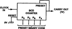
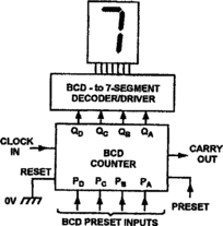
Figure 12.9 shows one basic way of using the PRESET function in a counter. Here, the 7-segment readout displays the current preset BCD number while the PRESET control is activated, and the counter then counts up from that number when the PRESET control is deactivated; the BCD inputs may be derived from special switches, or may be taken from the BCD outputs of a slowly clocked up/down counter, etc. This latter technique is of special value in time-setting electronic clocks, etc.
Yet another use of the PRESET facility is as a master RESET control if the normal RESET is in permanent use as a divide-by controller; in this case the preset binary code is simply set to ‘0000’.
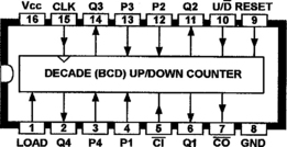
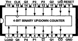
Several popular ‘up’-counter ICs are provided with programmable PRESET facilities. Among TTL types are the 74LS160, 74LS162 and 74LS196 decade counters, and the 74LS161, 74LS163 and 74LS197 4-bit binary counters; the most popular ‘4000’-series CMOS IC of this type is the 4018B (see Chapter 10). Most modern ‘down’- and ‘up/down’-counter/divider ICs are provided with programming facilities, and several examples of these are given in later sections of this chapter.
‘Down’ Counters
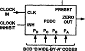
All ‘down’ counters should ideally have the basic facilities shown in Figure 12.10. Namely, they must be programmable (presettable) and have a special output that activates when the ‘zero’ count is reached, plus an input that inhibits the clocking action when activated. In the diagram, PRESET and INH (clock inhibit) are assumed to be active-high, and the ZERO OUT terminal goes high only when ZERO count is reached. In the following text and diagrams only decade (rather than binary) versions of these devices are considered, and the abbreviation ‘PDDC’ is used to indicate a programmable decade down counter.
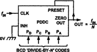
A PDDC can be used as a simple decade divider by connecting it as shown in Figure 12.11, with its PRESET and INH controls, etc., grounded, so that the counter repeatedly cycles through its basic BCD count, from 9 to 0 and then back to 9 again, and so on. The output, taken from the ZERO OUT terminal, goes high for one full clock cycle in every ten.
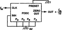
Figure 12.12 shows how to use a PDDC in its most important mode, as a programmable frequency divider. Here, the divide-by-N code is applied to the preset terminals and PRESET is controlled by the ZERO OUT terminal. Suppose that at the start of the count the BCD number 4 has been preset into the counter. On the arrival of the first clock pulse the counter decrements to 3, on the second pulse to 2, on the third to 1, and on the fourth to 0, at which point the ZERO OUT terminal goes high and presets the BCD number 4 back into the counter, so the whole sequence starts over again and ZERO OUT goes back low. Thus, the PDDC repeatedly counts by the number (4) set on the preset inputs, and the output (from the ZERO OUT terminal) takes the form of a narrow pulse with a width of a few tens of nanoseconds.
The really important thing about the Figure 12.12 circuit is that it automatically divides by whatever BCD number is set on the preset terminals (compare this action to that of the programmable ‘up’ counter of Figure 12.8, in which the preset BCD number is complexly related to the divide-by number). This feature is of special importance in what are known as ‘decade cascadable’ counter/divider applications, in which the overall division values are easily and directly programmable; Figures 12.13 and 12.14 illustrate the salient points of the subject.
![]()
Figure 12.13 When conventional counters are cascaded they give a final output equal to the product of the individual division values
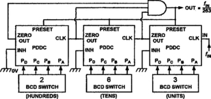
Figure 12.14 When PDDCs are wired in the decade cascaded mode they give a final ‘divide-by’ value equal to the sum of their individual decade values
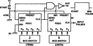
Figure 12.13 shows a conventional circuit in which three normal divider stages, with divide-by values of 2, 6 and 3, are cascaded to give an overall division value of 36, i.e. equal to the product of the individual divide-by values. Figure 12.14, on the other hand, shows what happens when PDDCs with divide-by values of (reading from left to right) 2, 6 and 3 are wired in the decade cascadable mode; in this case the overall divide-by value is equal to the sum of the individual decade values, and (since the decades are graded in ‘hundreds’, ‘tens’, and ‘units’) equals 263, or whatever other 3-digit number is set up on the PRESET switches. The circuit operates as follows.
Note in Figure 12.14 that the ZERO OUT signals of the three PDDCs are ANDed and used to drive the PRESET and OUT lines, which thus becomes active only when all three ZERO OUT signals coincide. With this point in mind, assume that at the start of the count cycle the BCD number 263 is loaded into the counters as shown. For the first few counts in the cycle the unit’s PDDC counts from 3 down to 0 and then goes into the normal 9-to-0 decade down-counting mode, passing a clock pulse on to the ‘tens’ PDDC each time the 0 state is reached. Thus, the ‘tens’ PDDC receives its first clock pulse after three input cycles and counts down from 6 to 5, but from then on is clocked down one step for every ten input cycles, until its own count falls to zero, at which point it passes a clock pulse on to the hundreds counter and simultaneously goes into the decade down-counting mode. One hundred input cycles later the ‘hundreds’ PDDC receives another clock pulse and its own count falls to zero; one hundred input cycles after that (on the 263rd count of the cycle) it receives a third clock pulse, and at that instant the ZERO OUT signals of all three PDDCs are active, so the AND gate activates the PRESET line and loads the BCD number 263 back into the counters, and the whole sequence starts over again.
Thus, the Figure 12.14 circuit repeatedly divides by 263 or whatever other 3-decade number is programmed in, and produces a narrow output pulse (from the AND gate) on completion of each ‘divide-by-263’ counting cycle. This output pulse is only a few tens of nanoseconds wide (the width is dictated by the circuit’s propagation delays), but is wide enough to trigger digital elements such as counters or monostables, etc.
PDDC Applications
Decade cascaded PDDC circuits of the Figure 12.14 type have important practical applications in frequency synthesis, programmable counting, and programmable timing. In frequency synthesis the PDDCs are wired as a programmable frequency divider and used in conjunction with a phase-locked loop (PLL) as shown in Figure 12.15. Here, the output of a wide-range voltage-controlled oscillator (VCO) is fed, via the programmable divide-by-N counter, to one input of a phase detector, which has its other input taken from a crystal-controlled reference-frequency generator. The phase detector produces an output voltage proportional to the difference between the two input frequencies; this voltage is filtered and fed back to the VCO control in such a way that the VCO automatically self-adjusts to bring the variable input frequency of the phase detector to the same value as the reference frequency, at which point the PLL is said to be ‘locked’.
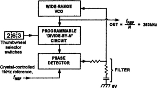
Figure 12.15 A programmable divide-by-N circuit can be used in conjunction with a PLL to make a precision programmable frequency synthesizer
Note that, when the PLL is locked, the VCO’s output frequency is N times that on the variable input of the phase detector, and is thus N times that of the reference generator, e.g. if N = 263 and fREF = 1kHz, fOUT = 263kHz, and has crystal precision. Thus, this circuit can be used to generate precise output frequencies that are variable in 1kHz steps via the 3-decade thumbwheel selector switches.
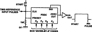
Figure 12.16 shows, in basic form, how a single PDDC can be used as a simple counting circuit. Here, the INH terminal is connected directly to ZERO OUT, so that the PDDC’s clocking action is inhibited when the PDDC is in the ‘0’ counting state; normally, the circuit is locked into this state, with its output at the logic-1 level. Suppose now that the BCD number 6 is preset via the START button; the output immediately switches low, and on the arrival of each clock pulse the PDDC counts down one step until finally, on the arrival of the sixth pulse, the ZERO OUT terminal goes high again and activates INH, causing any further pulses to be ignored. The count sequence is then complete, but can be restarted via the START button.
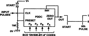
Figure 12.17 shows how the basic circuit can be turned into a useful 2-decade unit that can be programmed to count by any number up to 99 and has an output that goes high for the full duration of the counting cycle. This type of circuit is useful in (for example) controlling automatic packing machines in applications where N objects have to be loaded into each container, but the N value is often varied. In such an application, the object feeder must generate a clock pulse each time it feeds an object into the container, and must be so arranged that it directs its feed to the next container when the first one is registered ‘full’.
Finally, Figure 12.18 shows, in basic form, how the simple Figure 12.16 circuit can be made to act as a programmable timer with an output that goes high as the START button is pressed but then goes low again a preset time later. Here, the clock signal (which ideally should be synchronized with the START signal) is taken from a time-reference source (e.g. 1 pulse per second or minute, etc.). This basic circuit can be expanded to two decades by using connections similar to those of Figure 12.17.
Practical PDDC circuits can be built by using either dedicated programmable down-counter ICs, or by using up/down counters wired into the down-counting mode. No dedicated programmable ‘down’ counters are available in TTL form, but several are available in CMOS form, the best known examples being the 4522B and 4526B ‘Single’ and the 40102B (or 74HC40102) and 40103B (or 74HC40103) ‘Dual’ ICs, which are described in the next two sections of this chapter.
The 4522B and 4526B ICs
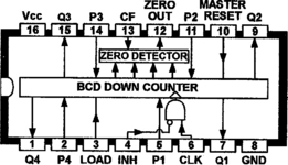
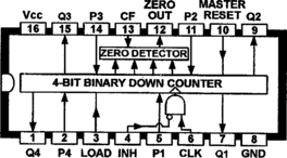
The best known family of CMOS programmable cascadable down counters comprise the 4522B (BCD decimal) and the 4526B (binary) 4-bit ICs, which have the functional diagrams shown in Figures 12.19 and 12.20. Each of these ICs contains a 4-bit down counter that has its Q1 to Q4 outputs externally available and can be synchronously reset to zero by taking the MASTER RESET pin high, and which can be loaded with a 4-bit ‘divide-by’ code (applied to the P1 to P4 pins) via the pin-3 LOAD control. The counter clock (CLK) signal can be inhibited via the INH terminal. An AND gate is built into the ZERO output line, so that the ZERO output can only go high if the CASCADE FEEDBACK (CF) terminal is also high, thus enabling cascading to be achieved without the use of external gates.
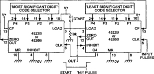
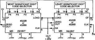
The 4522B decade down counter can be used as a PDDC in the same basic ways as shown in Figures 12.11 to 12.18, except that the MASTER RESET pin is normally grounded and the AND gate is already built into the IC. When the IC is used alone, the CASCADE FEEDBACK (CF) terminal must be tied high to enable the ZERO output. When cascading two or more ICs, tie the ZERO output of the MSD package to the CF terminal of the (MSD – 1) package, repeating the process on all less-significant dividers except the first. Figure 12.21 shows practical connections for making a 2-stage programmable down counter, and Figure 12.22 shows the connections for a 2-stage programmable frequency divider, using either 4522B or 4526B ICs.
When using these ICs, note that all unused inputs (including PRESETs) must be tied high or low, as appropriate, and that the outputs of all internal counter stages are available via the Q terminals, enabling the counter states to be decoded via external circuitry.
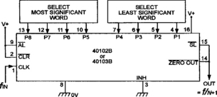
The 40102B and 40103B ICs
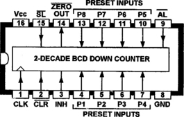
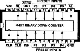
The 40102B and 40103B are another popular family of CMOS programmable cascadable down-counter ICs, but in this case each device houses a cascaded pair of presettable 4-bit down counters, with only the NOT-ZERO output (which goes low under the zero count condition) of the counters externally available; Q outputs are not provided. Figure 12.23 shows the functional diagram of the 40102B (and its ‘74HC’-series counterpart, the 74HC40102), which functions as a 2-decade BCD-type down counter, and Figure 12.24 shows the functional diagram of the 40103B (and 74HC40103), which functions as an 8-bit binary down counter. Both types clock down on the positive transition of the CLK signal. Figure 12.25 shows the Truth Table that is common to both ICs.
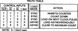
Codes that are applied to the eight PRESET pins of the ICs can be loaded asynchronously by pulling the NOT-AL pin low, or synchronously (on the arrival of the next CLK pulse) by pulling the NOT-SL pin low. When the NOT-CLR input is pulled low the counter asynchronously clears to its maximum count. When the inhibit (INH) control is pulled high it inhibits both the clock counting action and the NOT-ZERO output action, thereby acting as a ‘carry-in’ terminal in cascaded applications.
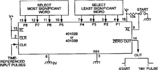
Figures 12.26 to 12.29 show four basic ways of using this family (or their ‘74HC’-series counterparts) of presettable down counters. Figure 12.26 shows the connections for making a programmable 8-bit or 2-decade timer or down counter, and Figure 12.27 shows the circuit of a programmable frequency divider. The latter circuit gives divide-by-(N + 1) operation, its output going low for one full clock cycle under the ‘zero count’ condition; true divide-by-N operation can be obtained by tying the NOT-SL pin high and wiring the NOT-ZERO output (pin-14) to NOT-AL (pin-9), but in this case the output pulses have widths of only a few hundred nanoseconds.
Finally, Figures 12.28 and 12.29 show the basic connections that are used to cascade 40102B or 40103B stages in large-bit programmable applications. The Figure 12.28 connections give ripple operation, and the Figure 12.29 connections give fully synchronous operation (for high-speed applications).
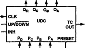
‘Up/down’ Counters
‘Up/down’ counters (UDCs) are the most versatile of all counter types. They are invariably programmable and synchronous in operation, are available in both BCD decade and 4-bit binary counting forms, and in most cases have the basic facilities shown in Figure 12.30, i.e. they have PRESET inputs and a full set of Q outputs, can be set to clock up or down via a single UP/NOT-DOWN terminal, have a clock inhibit (INH) facility, and have a TC OUT output that becomes active when the counter reaches its Terminal Count (‘0’ in down-counting mode, ‘9’ in decade up-counting mode, etc.). The 40192B and 74LS/HC192 (BCD decade) and 40193B and 74LS/HC193 (4-bit binary) UDCs differ from this norm in that they use separate ‘up’ and ‘down’ clocks and have no master INH facility, but are otherwise similar. Individual UDC IC types differ mainly in their pin terminology (the INH terminal may, for example, be named NOT-ENABLE or CARRY IN, etc.) and in their details of use, i.e. INH or TC OUT may be active-high on one IC type and active-low on another.
Because of their versatility and consequent high sales volumes, up/down counters are often available at lower cost than conventional types, and can thus be used instead of normal or programmable ‘up’ or ‘down’ counters in a wide range of applications, as well as being invaluable in add/subtract and up/down differential counting applications, etc. Figures 12.31 to 12.41 show a selection of different ways of using the basic Figure 12.30 UDC; in these diagrams it is assumed that the INH, PRESET and TC OUT controls are active-high, and that the IC counts up when the UP/NOT-DOWN control is biased high, and down when it is biased low.
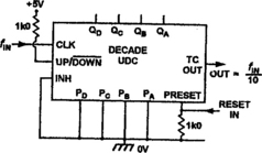
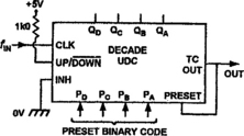
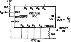
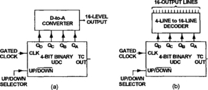
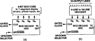
Figure 12.35 Basic ways of using a BCD decade UDC as (a) a 4-bit BCD code generator or (b) a multi-line selector
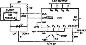
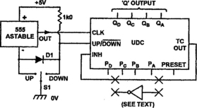
Figure 12.37 Typical circuit of a gate-clocked ‘end-stopped’ UDC circuit (PRESET connections not shown)
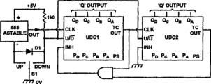
Figure 12.38 Basic method of expanding the Figure 12.37 end-stopped UDC circuit to give an 8-bit output
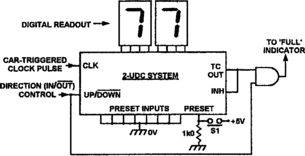
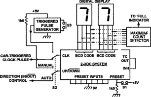
Figure 12.40 Improved car park ‘number-of-cars-parked’ indicator can show any ‘FULL’ value up to 99 maximum
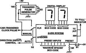
Figure 12.31 shows a decade up/down counter used as a simple decade up counter/divider, in which PRESET can be used as a RESET control that forces the outputs into the 0000 state when it is taken high. Figure 12.32 shows the UDC used as a programmable up divider of the Figure 12.8 type, and Figure 12.33 shows it wired as a programmable frequency divider of the far more useful Figure 12.12 down-counting PDDC type, in which the divide-by value equals the BCD value set on the programming terminals; this basic down-counter circuit can easily be used in the decade cascaded modes shown in Figures 12.14 and 12.17, etc.
Figure 12.34 shows, in basic form, how a 4-bit Binary UDC can be used as (a) a digital-to-analogue converter (DAC) driver or (b) a multi-line selector. The DAC driver produces 16 selectable output voltage levels when driven by the 4-bit Binary UDC as shown, or 256 levels if two UDCs are cascaded to give 8-bit DAC drive; these output voltage levels can easily be used to control sound levels or lamp brightness, etc., via suitable adaptor circuitry. The (b) circuit can be used as a multi-line selector, in which only one of the 16 output lines is active (usually active-low) at any one time, by using the UDC to drive a 4-line to 16-line decoder as shown, or can be used like a single-pole 16-way switch by using it to drive a CMOS analogue switch IC such as the 4067B, etc.
Figure 12.35 shows, in basic form, how a BCD decade UDC can be used as (a) a 4-bit BCD code generator or (b) a multi-line selector. In the former case the BCD code can be used to drive PRESET inputs and/or 7-segment digital displays, etc., and the circuit is thus useful in the time setting of clocks and presetting of counters, etc. The (b) circuit can be used in the same ways as the multi-line selector of Figure 12.34, but gives only ten outputs; its BCD output can, however, be used to simultaneously drive a digital display that shows the prevailing output number. Also, by using multiplexing or ANDing techniques, two of these basic circuits can be cascaded to make up to one hundred individual outputs available.
Figure 12.36 shows typical connections that may be used in practical versions of the Figure 12.34 or 12.35 gate-clocked circuits. Here, a 555 IC is used in the astable mode as a clock-waveform generator, and is normally disabled but can be gated on by grounding its negative supply line via centre-biased toggle switch S1, which also controls the UDC’s up/down direction. The UDC’s preset inputs are shown configured so that they give codes of 0000 (= BCD ‘0’) when S2 is closed or 1111 (= terminal count in Binary up-counting mode) when S2 is open, enabling a Binary UDC to be instantly set to either end of its counting range.
Note that the Figure 12.36 circuit gives a ‘free-ranging’ clocking action, i.e. when it reaches the terminal count in a clocking cycle it automatically jumps back to the ‘start’ count on the arrival of the next clock pulse. A popular alternative to this is an ‘end-stopped’ counting action, in which counting automatically ceases when the terminal count is reached, and can only be restored by reversing the count direction, i.e. so that a lower number can only be reached by clocking down, and a higher number can only be reached by clocking up. If the UDC’s INH and TC OUT terminals have the same active states (both active-high or active-low) this action can be obtained by simply shorting these two terminals together as shown in Figure 12.37, but if they have opposite active states an inverter stage must be wired between TC OUT and INH as indicated in the diagram (the UDC’s ‘preset’ connections are not shown in the diagram).
The basic Figure 12.36 free-ranging circuit can be expanded to give an 8-bit output by cascading it with another UDC, with both INH terminals grounded and with both UP/NOT-DOWN terminals shorted together, etc., and with the TC OUT of the first UDC providing the CLK signal of the second IC. The procedure for expanding the end-stopped version is a little more complex, as shown in Figure 12.38. In this case both UP/NOT-DOWN terminals are again shorted together, and the TC OUT of UDC1 provides the CLK signal for UDC2, but the TC OUTs of both counters are ANDed and fed to INH of UDC1, thus providing bi-directional end-stopping, and INH of UDC2 is grounded. Note in these expanded circuits that the first UDC (UDC1) provides the four least-significant bits of the 8-bit output.
‘Add/subtract’ Circuits
A UDC can be made to perform add/subtract actions by simply switching it to the up mode for addition or the down mode for subtraction and clocking in one input pulse per add or subtract unit. This type of action is useful in applications such as car park monitoring, etc., and Figure 9.39 shows the basic circuit of a monitor that keeps track of the number of cars in a car park with a maximum capacity of 99 vehicles. Assume here that the car park’s entry/exit is fitted with a system that generates a single clock pulse and a logic-1 level whenever a vehicle enters the site, and a single pulse and a logic-0 level whenever a vehicle leaves the site, and is fitted with fool-proof logic circuitry that ensures that only one of these sets of states can occur at any given moment. Also assume that the circuit uses two UDCs connected in the end-stopped counting fashion shown in Figure 12.38, and thus cannot count below zero or above 99; the basic circuit operates as follows.
At the start of each day the car park attendant operates PRESET switch S1, setting the digital readouts to zero. The readout then increments by one count each time a vehicle enters the car park or decrements by one count each time a vehicle leaves, thus giving a running count of the number of vehicles parked; when this number reaches 99, the TC OUT and UP/NOT-DOWN terminals are both at logic-1 and are ANDed and used to activate the car park’s ‘FULL’ sign (note that this AND gate stops the ‘FULL’ sign activating when TC OUT goes high at zero count in the down mode).
The basic Figure 12.39 circuit has two obvious defects. First, it has no facility for correcting counting errors, such as occur if the attendant activates the PRESET switch without realizing that a number of vehicles remained locked in overnight. Second, it only activates the ‘FULL’ sign correctly if the car park has a maximum capacity of 99 vehicles. Figure 12.40 shows how both of these defects can be overcome. Here, S2 is a biased 2-pole toggle switch that is normally set to AUTO; any start-of-the-day counting errors can be rectified – after setting the count to zero via S1 – by moving S2 to the MANUAL position and feeding in manually triggered clock UP pulses via S3 until the reading is correct. The second defect is overcome by a set of gates connected as a MAXIMUM-COUNT DETECTOR, which gives a logic-1 output and activates the ‘FULL’ sign only when the system’s two 4-bit BCD output codes correspond with the car park’s maximum capacity.
An alternative – and probably better – approach to the ‘car park’ problem is to have a system that displays the available number of parking spaces, rather than the number of parked cars. Figure 12.41 shows a basic circuit of this type. Here, the car park’s entry/exit system is made to generate a low (down-count) level when a car enters, and a high (up-count) level when a car leaves. When the S1 PRESET switch is operated it loads the car park’s BCD ‘maximum number of spaces’ code into the system, and this number appears on the display; any real-life errors in this ‘spaces’ reading can be corrected by setting S2 to MANUAL and operating S3. The ‘spaces’ readout then decrements by one count each time a car enters the car park or increments by one count each time a car leaves, thus giving a running count of the number of available spaces; when this number falls to zero the TC OUT terminal goes high and activates the car park’s ‘FULL’ sign (note that this sign will also activate if the ‘spaces’ count rises to 99, so this circuit functions correctly up to a maximum ‘spaces’ value of only 98, unless suitably modified; the maximum capacity can easily be expanded to 998 spaces, by basing the design on 3-UDC system).
‘Up/down’ Counter ICs
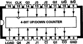
Several different up/down-counter ICs are readily available in CMOS and TTL forms. In ordinary CMOS, the 4029B, 4510B, 4516B, 40192B and 40193B are very popular. The 4029B is unusual in that it has a control terminal that enables it to count in either decade or binary mode; the 4510B decade and 4516B binary counters are single-clock ICs with identical pin notations, and the 40192B decade and 40193B binary counters are dual-clock ICs with identical pin notations; four of these ICs are also available in the ‘74HC’-series as the 74HC4510, 74HC4516, 74HC40192, and 74HC40193.
In the ‘74LS’-TTL series, the most popular up/down counters are the 74LS190 and 74LS192 ‘decade’ types and the 74LS191 and 74LS193 ‘binary’ types. Of these, the ‘190’ and ‘191’ are single-clock ICs with identical pin-outs and control functions, and the ‘192’ and ‘193’ are dual-clock types with identical pin-outs and control functions. These four counters are also available in ‘74HC’-series CMOS versions, as the 74HC190, 74HC191, 74HC192, and 74HC193.
All of the above ICs are described in greater detail in the remaining sections of this chapter.
The 4029B UDC IC
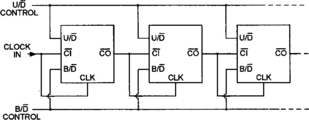
Figure 12.42 shows the functional diagram of the 4029B presettable up/down-counter IC, and Figure 12.43 shows the basic usage circuit of this very versatile device, which acts as a binary counter when the B/NOT-D (pin-9) terminal is high, or as a decade counter (with BCD ‘Q’ outputs) when the terminal is low. The IC counts up when the U/NOT-D (pin-10) terminal is high, or down when the terminal is low (note, however, that this terminal should only be changed when the clock signal is high). The LOAD terminal is normally held low; it forces the outputs to immediately (asynchronously) agree with the binary code set on the ‘J’ inputs when it is taken high.
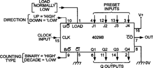
The IC’s NOT-CI (pin-5) ‘carry in’ terminal is actually a clock disabling input, and is held low for normal clocking operation. When NOT-CI and LOAD are low, the counter shifts (up or down) one count on each rising edge of the clock signal. The NOT-CO (pin-7) ‘carry out’ terminal of the IC is normally high and goes low only when the counter reaches its maximum count in the up mode or its minimum count in the down mode (provided that the NOT-CI input is low).
The actions of the 4029B’s NOT-CI and NOT-CO terminals are designed to facilitate fully synchronous clocking in multi-stage counting applications, as shown in the basic circuit of Figure 12.44, where all ICs are clocked in parallel and the NOT-CO terminal of each counter is used to enable the following one (at a ‘one-tenth of’ rate) via its NOT-CI terminal.
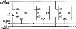
Numbers of 4029Bs can also be cascaded and clocked in the asynchronous ripple mode by using the basic connections shown in Figure 12.45, but in this case the Q outputs of different counters may not be glitch-free when decoded. Note in this diagram that the CLK and NOT-CI terminals are joined together on each IC, to ensure that false counting will not occur if the U/NOT-D input is changed during a terminal count.
The 4510B and 4516B UDC ICs
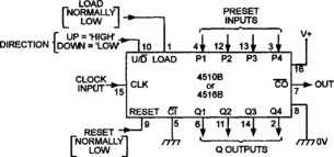
The 4510B and 4516B are single-clock presettable up/down counters. The 4510B (and its ‘HC’ equivalent, the 74HC4510) is a 4-bit decade counter with BCD outputs, and the 4516B (and 74HC4516) is a 4-bit binary counter. The ICs have the functional diagrams shown in Figures 12.46 and 12.47, and have a RESET terminal which is held low for normal operation but sets all Q outputs to ‘0’ (cleared) when biased high. The outputs can be forced to agree with the binary code preset on the ‘P’ terminals by applying a logic-1 level to the LOAD (pin-1) terminal. The ICs count up when the U/NOT-D terminal (pin-10) is high, and down when the terminal is low; the U/NOT-D input must only change when the clock signal is high. Figure 12.48 shows the basic usage circuit that applies to this family of ICs.
The NOT-CI (pin-5) terminal is actually a clock disabling input, and is held low for normal operation. When NOT-CI (and RESET and LOAD) is low, the counter shifts one count on each rising edge of the clock signal. The NOT-CO (pin-7) terminal is normally high and goes low only when the counter reaches its maximum count in the up mode or its minimum count in the down mode (provided that the NOT-CI terminal is low).
Numbers of 4510Bs or 4516Bs (etc.) can be cascaded and clocked in parallel to give fully synchronous action by using the basic connections shown in Figure 12.49, or can be cascaded in the asynchronous ripple mode by using the basic connections of Figure 12.50, which ensures counting validity even if the U/NOT-D input is changed during a terminal count.
The 40192B and 40193B UDC ICs
The 40192B and 40193B are dual-clock presettable up/down counters. The 40192B (and its ‘HC’ equivalent, the 74HC40192) is a 4-bit decade counter with BCD outputs, and the 40193B (and 74HC40193) is a 4-bit binary counter. The ICs have the functional diagrams shown in Figures 12.51 and 12.52, and have a RESET terminal which is held low for normal operation but sets all Q outputs to ‘0’ (cleared) when biased high. The outputs can be forced to agree with the binary code preset on the ‘J’ terminals by applying a logic-0 level to the NOT-LOAD (pin-11) terminal, which is normally biased high.
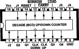
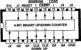
The counters have two clock lines, one controlling the up count and the other controlling the down count. Only one clock terminal must be used at a time; the unused input must be biased high. The counter shifts one count (up or down) on each rising edge of the used clock line. The NOT-CARRY (pin-12) and NOT-BORROW (pin-13) outputs of the counters are normally high, but the NOT-CARRY output goes low one-half clock cycle after the counter reaches its maximum count in the up mode, and the NOT-BORROW output goes low one-half clock cycle after the counter reaches its minimum count in the down mode.
Figure 12.53 shows the basic way of wiring the 40192B or 40193B (etc.) in cascaded multiple IC applications.
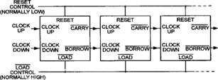
The NOT-BORROW and NOT-CARRY outputs of each IC are simply connected directly to the CLK DOWN and CLK UP inputs respectively of the following ICs.
The 74LS/HC190 and 74LS/HC191 UDC ICs
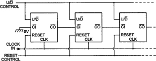
Figure 12.54 shows the functional diagrams and pin-outs of the 74LS190 and 74LS191 single-clock up/down counters (and their fast CMOS equivalents, the 74HC190 and 74HC191). These two ICs have very similar active characteristics; namely, they trigger on the rising edge of the clock signal, and count up when pin-5 is low or down when pin-5 is high (assuming that INH is low and NOT-PRESET is high); the TC OUT terminal is normally low, but goes high for one clock cycle when the IC reaches its terminal count (0 in the down mode, or, in the up mode, 9 in the 74LS190 or 15 in the 74LS191). Note that both ICs have a terminal notated NOT-RC; this ‘ripple clock’ terminal is normally high but goes low on the falling edge of the terminal count and goes high again on the next clock rising edge; the terminal provides a clean clocking signal in multi-stage circuits, and is used as shown in Figures 12.55 and 12.56.
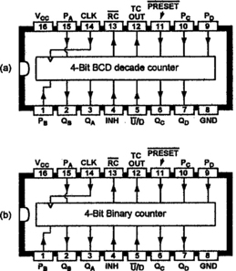
Figure 12.54 Functional diagrams of the (a) 74LS/HC190 decade and (b) 74LS/HC191 binary 4-bit up/down-counter ICs
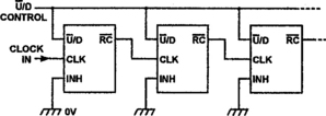
Figure 12.55 Basic ways of using the 74LS/HC190 or 74LS/HC191 as an N-stage ripple-clocked up/down counter (with NOT-PRESET at logic-1)
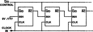
Figure 12.56 Basic ways of using the 74LS/HC190 or 74LS/HC191 as an N-stage synchronously clocked up/down-counter (with NOT-PRESET at logic-1)
Figure 12.55 shows the basic way of using the ‘190’ or ‘191’ as multi-stage up/down counters, using ripple clocking; in essence, the ripple clock signal of the first counter acts as the clock of the second stage, and the ripple clock of that acts as the clock of the third stage, and so on for however many stages there are. Figure 12.56 shows how to use the counters in the fully synchronous clocking mode; in this case all ICs are clocked in parallel, but the ripple clock output of each stage controls the INH action of the next stage. Note that the NOT-PRESET control is not shown in these two circuits, but should be tied to logic-1 for normal clocked operation.
The 74LS/HC192 and 74LS/HC193 UDC ICs
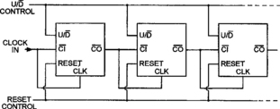
Figure 12.57 shows the functional diagrams and pin-outs of the 74LS192 and 74LS193 dual-clock up/down counters (and their fast CMOS equivalents, the 74HC192 and 74HC193). These ICs have similar active characteristics; they trigger on the rising edge of the clock signal, and count up when the clock signal is applied to pin-5, or down when it is applied to pin-4; only one clock line must be used at a time, and the inactive one must be tied high. The CLK CARRY ‘UP’ and ‘DOWN’ outputs are normally high terminal count outputs that are useful in multi-stage ripple clocking applications; the ‘UP’ output goes low on the falling edge following the ‘UP’ terminal count, and returns high on the next rising edge; the ‘DOWN’ output similarly goes low, etc., on the ‘DOWN’ terminal count of ‘0’. The CLR terminal is normally low, and sets all Q outputs to ‘0’ when taken high; NOT-PRESET is normally high, and loads the PRESET data when taken low.
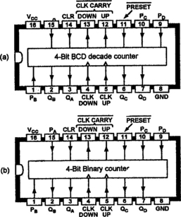
Figure 12.57 Functional diagrams of the (a) 74LS/HC192 decade and (b) 74LS/HC193 binary 4-bit dual-clock up/down-counter ICs
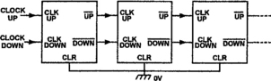
Figure 12.58 shows the basic way of using the ‘192’ or ‘193’ as multi-stage up/down counters, using ripple clocking; here, the ‘CLK CARRY’ ‘UP’ and ‘DOWN’ outputs of the first counter act as the ‘UP’ and ‘DOWN’ clocks of the second stage, and the ‘CLK CARRY’ outputs of that stage act as the clocks of the third stage, and so on for however many stages there are. Note that the CLR terminal is tied low for normal operation; the NOT-PRESET control isn’t shown, but should be tied to logic-1 for normal clocked operation.
Counter Conversions
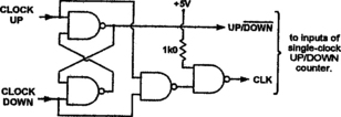
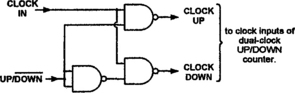
In most practical applications a dual-clock UDC has no intrinsic advantage over a single-clock type, or vice versa, and one type can easily be made to act like the other by using suitable input conversion logic circuitry. Figure 12.59 shows a converter that makes a dual-clock counter act like a single-clock type (the circuit is shown set for 5V operation), and Figure 12.60 shows a converter that enables a single-clock counter to be driven in the dual-clock mode; in multi-stage counters, these converters must be applied to the input(s) of the first stage only. If the counter’s up/down ‘active’ levels are the reverse of those shown in the diagrams, simply reverse the input connections to the circuit in Figure 12.59, or reverse the output connections from the circuit in Figure 12.60.