Latches, Registers, Comparators and Converters
Data latches and shift registers are widely used members of the flip-flop family of devices, and are often used in conjunction with logic comparators and code converters. This chapter looks at LS TTL and CMOS versions of all of these devices and shows how to use them.
Data Latches
Flip-flop circuit elements of the SET-RESET, D-type, and JK types (see Chapter 10) are often called ‘latches’, because their outputs can be latched into either a logic-0 or logic-1 state by applying suitable input signals. JK and D-type latches are fairly versatile elements, and can be made to act as either data latches or as divide-by-2 circuits by suitably connecting their input and output terminals. A pure ‘data latch’, on the other hand, is an element that is built as a dedicated data latch and can be used for no other purpose; an element of this type acts as a simple memory that can store one ‘bit’ of binary data for an indefinite period; four such elements can store a complete 4-bit binary ‘word’.
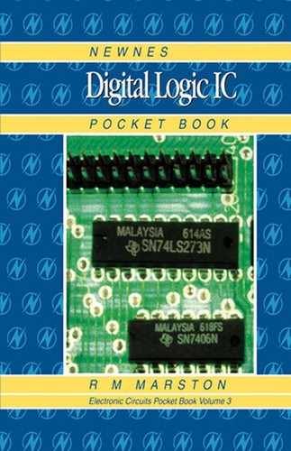
A data latch stores and outputs whatever logic level is applied to its ‘D’ (data) terminal when activated by a suitable ‘store’ command; the ‘store’ terminal may be either level or edge sensitive, and Figure 13.1 shows the basic data latch symbols that apply in each case. Level-triggered elements of the Figure 13.1(a) type are ‘transparent’ when the En (enable) terminal is high (i.e. the Q output follows the D input under this condition), but latch the prevailing D state into the Q output when En goes low; data can thus be latched by applying a brief positive pulse to the En terminal. Edge-triggered elements of the Figure 13.1(b) type are not transparent, and the Q output ignores the D input until a clock-pulse trigger edge is applied to the CLK input, at which point the latch stores and outputs the data and holds it until a new clock pulse arrives.
A 4-bit data latch can be built by connecting four 1-bit latches together as shown in Figure 13.2, with all En (or CLK) terminals wired in parallel so that all elements activate at the same time. Edge-triggered 4-bit data latches are not as useful, popular, or as readily available as level-triggered types, but can easily be built from JK or D-type flip-flop ICs such as the 74LS73, 74LS74, 4013B or 4027B, etc. Level-triggered 4-bit or greater transparent data latch ICs are readily available, at low cost.

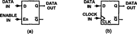
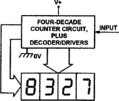
Level-triggered 4-bit data latches are widely used as temporary memories in digital display-driving applications, and may be used in either of the two basic ways shown in Figure 13.3. Assume here that the decade counter shown is one of a cascaded chain of such counters, each of which has its BCD outputs fed to a 7-segment digital display via a 4-bit data latch and a decoder/driver IC, as shown. In simple counting applications the data latch may be used as in (a), with its En terminal connected to the V+ rail via a 4k7 resistor so that it is biased high when S1 is set to the ENABLE position but is grounded when S1 is in the FREEZE position. Thus, in the ENABLE position the Latch is transparent, and the counter’s state is instantly shown on the display (which may appear as a blur if fast counting is taking place), but when S1 is moved to the FREEZE position the data is immediately latched and the display is effectively frozen (i.e. changes in the counter’s states are no longer displayed).

In the alternative control mode shown in (b), the data latch’s En terminal is fed with a timed chain of positive LATCH DATA pulses, and the display thus shows a grabbed snapshot of the counter’s instantaneous state each time one of these pulses terminates, and displays it until the arrival of the next pulse’s termination point. This technique is useful in cases where the display normally appears as a fast-changing blur; by feeding in the LATCH DATA pulses at (say) a ten-per-second (100ms) rate, the display can be strobed so that it appears in a varying but clearly readable form. This technique is widely used in digital frequency meters, which use the basic operating principle shown in Figure 13.4.
The Figure 13.4 circuit is that of a simple 3-digit frequency meter in which the test frequency is fed to the input of the counter chain via a 2-input AND gate, which is controlled via a timebase generator that produces a repeating timing cycle. At the start of this cycle the gate is closed, and a brief RESET pulse is fed to all three counters, which clear to zero; the gate then opens, and the counters start to sum the input signal pulses. This count continues for precisely one second, during which the 4-bit data latches prevent the counter outputs from reaching the display. At the end of the one-second timing period the GATE closes and terminates the count, and simultaneously an En pulse is fed to the set of data latches; this pulse has a width of (say) 100ns or greater, so all the counters have settled down and any glitches have disappeared by the time the En pulse terminates and latches the summed one-second end-count, which is fed to the display and reveals the input test signal’s frequency, in Hz (cycles per second). The timing sequence is then complete, but a few moments later it starts to repeat, with the counters resetting and then counting the input pulses for another second, during which time the display gives a steady reading of the results of the previous count, and so on.
The Figure 13.4 circuit thus generates a stable ‘frequency’ display that is regularly updated. In practice, the actual count period can be made any decade multiple or submultiple of one second, provided that the output display is suitably scaled. Thus, on a 3-digit display, a ‘count’ period of one second gives a maximum frequency reading of 999Hz, and a 1mS period gives a maximum frequency reading of 999kHz, and so on.
Data Latch ICs
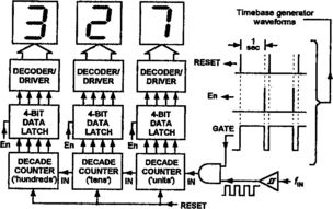
The most popular and readily available TTL 4-bit transparent (level-triggered) data latch IC is the 74LS75, which has the functional diagram, etc., shown in Figure 13.5. Note the unusual positions of this IC’s power supply pins, and also note that the less readily available 74LS375 4-bit data latch IC is internally identical to the 74LS75, but has normal power supply pin allocations, as shown in Figure 13.6. Both of these ICs in fact house two independent 2-bit data latches, but can be made to function as standard 4-bit data latches of the Figure 13.2 type (which are transparent when En is high but latch when En is low) by simply joining their En pins together; Figures 13.7(a) and (b) show the basic connections.


Figure 13.7 Way of using the (a) 74LS75 (or 74HC75) or (b) 74LS375 (or 74HC375) as a basic 4-bit data latch
Note that both of these ICs have a full set of Q and NOT-Q outputs, enabling any individual 4-bit code to be decoded via a 4-input AND (or NAND) gate. The BCD number ‘9’, for example, has the DCBA binary code ‘1001’, so can be decoded by simply ANDing the QD, NOT-QC, NOT-QB and QA outputs, which all go high when BCD ‘9’ is present.
If you need an 8-bit level-triggered LS TTL data latch and don’t need NOT-Q outputs, or do need 3-state outputs, the cheapest option is to use the 74LS373, which has the functional diagram shown in Figure 13.8. This 8-bit latch is transparent when the En terminal is high and latches when it is low; the outputs can be set into the high-impedance (3-state) mode by biasing pin-1 high (this pin must be biased low for normal operation).

Several transparent data latch ICs are available in the ‘74HC’-series CMOS range, three of the most popular being the 74HC75 and 74HC375 4-bit types and the 74HC373 8-bit type. These are simply fast CMOS versions of the 74LS75, 74LS375 and 74LS373 respectively and have identical functional diagrams to those ICs.
Very few transparent data latch ICs are available in the ‘4000B’-series CMOS range. The best known example is the 4042B 4-bit data latch, which has the functional diagram and Truth Table shown in Figure 13.9. The four latches in this IC are controlled via a single ENABLE (En) terminal, and the device is unusual in that it provides the option, via its pin-6 POL (polarity) terminal, of either normal or inverted ENABLE action, as indicated in the Truth Table. Thus, if POL is set to logic-1, the latches are transparent when En is at logic-1 and latch the D data when En is at logic-0, but give the reverse of this action if POL is set to logic-0.

Before leaving this subject, note that transparent data latches are most widely used as elements in 7-segment digital display driving systems of the types already shown in Figures 13.3 and 13.4, and are often incorporated in dedicated ‘latch/decoder/7-segment-driver’ ICs; two CMOS ICs of this type are described later in this chapter.
Shift Registers
In digital electronics, a ‘register’ is an element that provides temporary storage for one or more bits of binary data; a ‘shift register’ is one in which the stored bits can be displaced within the register – one step at a time – by applying suitable clock pulses. The simplest type of shift register is that shown in Figure 13.10, which is a synchronous ‘bucket brigade’ data shifter of the type already shown (in Figure 10.40) and described in Chapter 10. Here, the bit of binary data present at the input of FF1 is passed to FF1’s output on the application of the first clock pulse, then to the output of FF2 on the second pulse, to the output of FF3 on the third pulse, and finally to the output of FF4 on the fourth pulse. The circuit can hold four bits of data at any given moment, and can store it indefinitely; when the data is needed, it can be clocked out (in serial form) by applying another set of clock pulses.
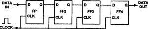
The Figure 13.10 circuit’s data is clocked in and out in serial form, so it is known as a serial-in/serial-out or SISO shift register; it is useful for storing binary signals or delaying them by a fixed number of clock pulses, but not for much else. Its value can be greatly increased by converting it to a serial-in/parallel-out (SIPO) shift register by simply taking the ‘parallel’ outputs from the Q terminals of all four flip-flops, as shown in Figure 13.11; it is then useful for converting serial data into parallel form. This basic type of register can be made to give both serial and parallel outputs by adding a ‘serial-out’ connection as shown dotted in the diagram; such a unit is known as a SIPO/SISO shift register.

The value of the basic shift register can be further increased by fitting it with PRESET terminals, as shown in Figure 13.12, so that it can be directly loaded with four bits of parallel data via pins P1 to P4. If the resulting circuit has no serial input facility, it is known as a parallel-in/serial-out (PISO) shift register, but if it does have a serial input facility (as shown dotted in the diagram) it is known as a PISO/SISO shift register. If it is configured to have only parallel-in and parallel-out facilities, it is known as a PIPO shift register. If a register has both parallel and serial inputs and parallel and serial outputs, it is simply called a ‘universal’ shift register.
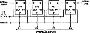
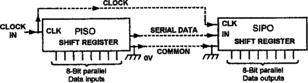
Figure 13.13 shows, in greatly simplified form, one widely used shift register application. Suppose here that a stack of 8-bit data words needs to be shifted from one point to another; normally, eight data links and one clock and one common link would be needed for this task, making a total of ten links, but by using shift registers the number of links can be reduced to three. This is achieved by first changing each 8-bit parallel word into serial form via a PISO shift register, then sending it and the clock and common signals down the 3-line link to be converted back into 8-bit parallel form via a SIPO shift register at the destination point, as shown. This same basic technique can be used for transferring multi-bit words into or out of modern memory or data processing ICs in which only single IN, OUT, CLK and COMMON pins are allocated to these tasks.
The basic shift registers of Figures 13.10 to 13.12 give an action in which the stored data shifts one step to the right on each application of a clock pulse, and are thus known as right-shift registers. But, just as an ordinary counter can be configured to count either up or down, a register can easily be configured to shift data to the right or left, or to have its direction selectable via a control terminal. A large variety of shift register configurations are thus possible.
In practice, most modern ‘74LS’-series shift register ICs are of the ‘universal’ type, one of the few exceptions being the 74LS164 8-bit SIPO shift register. Of the universal types, the 74LS195 is a plain 4-bit IC, the 74LS295 and 74LS395 are 4-bit types with 3-state outputs, the 74LS95 and 74LS194 are 4-bit right/left shift types, and the 74LS299 and 74LS323 are 8-bit types with 3-state outputs.
Among popular ‘74HC’-series types, the 74HC91 is an 8-stage SISO type, the 74HC164 is an 8-bit SIPO/SISO type, and the 74HC194 is a 4-bit bidirectional ‘universal’ type with CLEAR.
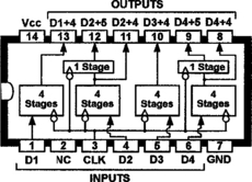
The oldest current-production ‘4000B’-series shift register IC is the 4006B, which the manufacturers simply describe as an ‘18-stage static shift register’. Figure 13.14 shows the functional diagram of this IC, which in fact houses four separate 4-stage shift registers, two of which are followed by an extra stage, with all stages controlled by a common clock signal that shifts data on its falling edges. The IC can be used as either a 4-bit PIPO type or (by cascading stages) as a SISO type with 4, 5, 8, 9, 10, 12, 13, 14, 16, 17, or 18 effective stages. (Note: On most versions of this IC, pin-2 is not internally connected, but on the RCA version it gives an extra D1 + 4 output that is delayed one-half clock cycle.)
Among other popular ‘4000B’-series types, the 4014B is an 8-stage PISO/SISO type, the 4015B is a Dual 4-stage SIPO type with RESET, the 4021B is an 8-stage PISO/SISO type, the 4031B is a 64-stage SISO type, the 4035B is a 4-bit PIPO type, and the 4094B is an 8-stage SIPO type with buffered 3-state outputs.
Logic Comparators
A digital ‘logic’ or ‘magnitude’ comparator IC is one that compares the binary codes of two words (A and B) of the same bit size and has outputs that indicate whether code A is greater than, smaller than, or equal to code B. This action is useful in, for example, triggering some action when a counting chain reaches a certain value, etc. The best known ICs of this type are the 74LS85, 74HC85 and 4063B 4-bit comparators (see Figure 13.15), which are functionally identical and which can be cascaded with others of their type to make a comparator of any desired bit size. Note that, as well as having four input terminals for each 4-bit word, plus three active-high output terminals (notated A > B, A = B, and A < B), this IC also has three input terminals (also notated A > B, A = B, and A < B) that are used to implement cascaded operations.
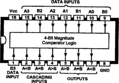
The 74LS/HC85 and 4063B are very easy to use, as shown in Figure 13.16. If only 4-bit words are being compared, a single IC is used, connected in the manner of IC1, with the A > B and A < B cascading terminals grounded and the A = B cascading terminal biased high, and with the three outputs taken from pins 5, 6 and 7. If the words have bit lengths that are whole-number multiples of four, they can be compared by cascading an appropriate number of 74LS/HC85 or 4063B on a basis of 4-bits per IC (e.g. three ICs for 12-bit comparison, etc.); in this case the four least-significant bits (LSBs) must be allocated to IC1, which must be connected in the way already described, and the four most-significant bits (MSBs) must be allocated to the final IC (ICN), and so on; in this case, the three outputs of each lower-order IC must be connected to the three ‘cascading’ inputs of the following IC, the final outputs being taken from the last IC in the chain.

Code Converters
Code converter ICs are widely used in digital electronics to change electronic codes from one format into another.
Some types (such as the 4514B and 4515B) are full 4-bit binary decoders, with an individual output for each of the 16 possible code numbers. Others (such as the 4028B) are 4-bit BCD-to-decimal decoders, with ten individual outputs. The most widely used type of converter is the BCD to 7-segment decoder/driver IC, which takes the 4-bit BCD output of a counter, etc., and converts it into a form suitable for directly driving a 7-segment LED or LCD digital display; some ICs of this type incorporate a 4-bit data latch that enables the display to be ‘frozen’. Before looking at specific ICs of these types, however, it is first necessary to note a few points about 7-segment digital display basics, as follows:
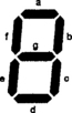
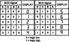
A 7-segment display is a unit that houses seven independently accessible photoelectric elements such as LEDs or liquid crystal segments, arranged in the form shown in Figure 13.17. The segments are conventionally notated from a to g in the manner shown, and they can be made to display any number from 0 to 9 or letter from A to F (in a mixture of upper and lower case) by activating these segments in various combinations, as shown in the Truth Table of Figure 13.18.

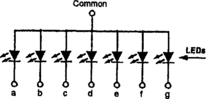
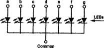
Practical 7-segment displays need at least eight external connectors, one of which acts as the ‘common’ terminal. If the display is an LED type, the seven individual LEDs may be arranged as shown in Figure 13.19, with all LED anodes connected to the common terminal, or as in Figure 13.20, with all LED cathodes connected to the common terminal; in the former case the 7-segment display unit is known as a common-anode type, and in the latter it is called a common-cathode type.
In most practical applications, 7-segment displays are driven – via a suitable decoder/driver IC – from a 4-bit BCD input, and the IC and display are connected as shown in Figure 13.21. The IC houses a moderately complex set of logic gates, as is implied by Figure 13.22, which shows the standard relationship between the BCD input codes and the displayed 7-segment numerals. In practice, BCD to 7-segment decoder/driver ICs are usually available in a dedicated form suitable for driving only a single type of display unit, e.g. a common-anode LED type, common-cathode LED type, or a liquid-crystal display (LCD). Figures 13.23 to 13.25 show the basic ways of interconnecting each of these IC and display types.

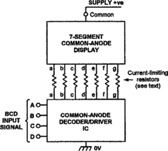
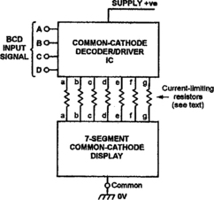

Note in the LED circuits that in most cases a current-limiting resistor (about 150R with a 5V supply, or 680R at 15V) must be wired in series with each display segment. To drive a common-anode display (Figure 13.23), the driver must have an active-low output, in which each segment-driving output is normally high, but goes low to turn a segment on. To drive a common-cathode display (Figure 13.24), the driver must have an active-high output.
In the Figure 13.25 LCD-driving circuit the display’s common BP (back-plane) terminal and the IC’s PHASE input terminal must be driven by a symmetrical squarewave (typically 30Hz to 200Hz) that switches fully between the two supply rail voltages (OV and V+), as shown. The full explanation for this is a little complicated, as follows.
To drive an LCD segment, the driving voltage must be applied between the segment and BP terminals. When the voltage is zero, the segment is effectively invisible. When the drive voltage has a significant positive or negative value, however, the segment becomes effectively visible, but if the drive voltage is sustained for more than a few hundred milliseconds the segment may become permanently visible and be of no further value. The way around this problem is, in principle, to drive the segment on via a perfectly symmetrical squarewave that switches alternately between identical positive and negative voltages, and thus has zero DC components and will not damage the LCD segment even if sustained permanently. In practice, this type of waveform is actually generated with the aid of an EX-OR True/Complement generator (see Chapter 6, Figure 6.97), connected as shown in Figure 13.26(a).
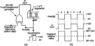
Figure 13.26 Basic LCD segment-drive circuit (a), and voltage-doubling ‘bridge-driven’ segment waveforms (b)
In Figure 13.26(a), the basic segment ‘a’ input drive (which is active-high) is connected to one input of the EX-OR element, and the other EX-OR input terminal (which is notated PHASE) is driven by a symmetrical squarewave that switches fully between the circuit’s supply rail voltages (shown as OV and + 10V) and is also applied to the LCD display’s BP pin. When the segment ‘a’ input drive is low, the EX-OR element gives a non-inverted (in-phase) ‘a’ output when the squarewave is at logic-0, and an inverted (anti-phase) ‘a’ output when the squarewave is at logic-1, and thus produces zero voltage difference between the ‘a’ segment and BP points under both these conditions; the segment is thus turned off under these conditions. When the segment ‘a’ input drive is high, the EX-OR element gives the same phase action as just described, but in this case the ‘a’ OUT pin is high and BP is low when the squarewave is at logic-0, and ‘a’ OUT is low and BP is high when the squarewave is at logic-1; the segment is thus turned on under these conditions.
Figure 13.26(b) shows the circuit waveforms that occur when the ‘a’ segment is turned on, with the ‘a’ segment and BP driven by anti-phase squarewaves. Thus, in part A of the waveform the segment is 10V positive to BP, and in part B it is 10V negative to BP, so the LCD is effectively driven by a squarewave with a peak-to-peak value of 20V but with zero DC value. This form of drive is generally known as a voltage-doubling ‘bridge drive’ system. In practice, many LCD-driving ICs (such as the 4543B) incorporate this type of drive system in the form of a 7-section EX-OR gate array interposed in series with the segment output pins, with access to its common line via a single PHASE terminal.
Note that any ‘active-high’ 7-segment LED-driving Decoder IC can be used to drive a 7-segment LCD display by interposing a ‘bridge driven’ 7-section EX-OR array (etc.) between its segment output pins and the segment pins of the LCD display, as shown in Figure 13.27, which shows a 7448 or 74LS48 TTL IC circuit so adapted.

Multi-digit Displays
In reality, 7-segment displays are usually used in multi-digit applications such as that shown in Figure 13.28, which shows the basic elements of a 4-digit counter/display circuit that can give a maximum reading of ‘9999’. Note that if this circuit is used to measure a count of (say) 27 it will actually give a reading of ‘0027’, unless steps are taken to automatically suppress the two (unwanted) leading zeros. Similarly, if the same display is used on a 4-digit voltmeter scaled to read a maximum of 9.999 volts, it will give a reading of 0.100 volts if fed with a 0.1 V input, unless steps are taken to suppress the two trailing zeros.
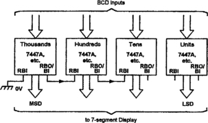
In practice, many modern decoder/driver ICs have facilities for giving automatic blanking of leading and/or trailing zeros, using the basic ripple-blanking techniques illustrated in Figures 13.29 and 13.30. Note in these diagrams that each decoder/driver IC is provided with ripple-blanking input (RBI) and output (RBO) terminals; if these terminals are active-high their actions are such that the IC gives normal decoder/driver action and RBO is disabled (driven low) when RBI is biased low, but the display is blanked and RBO is driven high under the ‘zero’ (BCD input ‘0000’) condition when RBI is biased high. Thus, the RBO terminal is normally low and goes high only if a BCD ‘0000’ input is present at the same time as the RBI terminal is high. With these facts in mind, refer now to Figures 13.29 and 13.30.
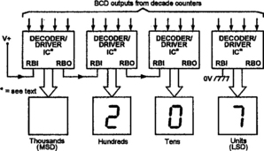
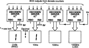
Figure 13.29 shows the ripple-blanking technique used to provide leading-zero suppression in a 4-digit display that is reading a count of 207. Here, the RBI input of the ‘thousands’ or MSD decoder/driver IC is tied high, so this display is automatically blanked and RBO is driven high in the presence of a zero. Consequently, RBI of the ‘hundreds’ IC is driven high under this condition; its display reads ‘2’ and its RBO terminal is thus low. The RBI input of the ‘tens’ unit is thus also low, so its display reads ‘0’ and its RBO output is low. The least significant digit (LSD) is that of the ‘units’ readout and does not require zero suppression, so its RBI input is grounded and it reads ‘7’. The display thus gives an overall reading of ‘207’.
Note in the Figure 13.29 leading-zero suppression circuit that ripple blanking feedback is applied backwards, from the MSD to the LSD. Figure 13.30 shows how trailing zero suppression can be obtained by reversing the direction of feedback, from the LSD to the MSD. Thus, when an input of 1.1V is fed to this circuit the LSD is blanked, since its BCD input is ‘0000’ and its RBI input is high. Its RBO terminal is high under this condition, so the ‘100ths’ digit is also blanked in the presence of a ‘0000’ input.
Not all decoder/driver ICs are provided with RBI and RBO ripple-blanking terminals, and some of those that are have an active-low action. If a decoder/driver IC does not incorporate a ripple-blanking feature, it can usually be obtained by adding external logic similar to that shown in Figure 13.31, with the RBO terminal connected to the blanking input pin of the decoder/driver IC. In Figure 13.31 (an active-high circuit), the output of the 4-input NOR gate goes high only in the presence of a ‘0000’ BCD input, and the RBO output goes high only if this input is present while RBI is high.

TTL Decoder/driver ICs
In TTL, the two most popular decoder/driver ICs are the old 7447A and 7448 types and their modern counterparts, the 74LS47 and 74LS48. These ICs are functionally very similar, as can be seen from Figures 13.32(a) and (b); all four ICs have integral ripple-blanking facilities. The 7447A/74LS47 has an active-low output and is specifically designed for driving a common-anode LED display via external current-limiting resistors RX (typically 150R), as shown in Figure 13.33. The 7448/74LS48 has an active-high output designed for driving a common-cathode LED display in a manner similar to that of Figure 13.33, but with the display’s common terminal taken to ground. In all cases, the RX current-limiting resistors must be chosen to hold the segment currents below the following absolute limits:
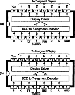
Figure 13.32 Functional diagrams of the (a) 7447A/74LS47 and (b) 7448/74LS48 BCD to 7-segment decoder/driver ICs

4774A =40mA; 74LS47 =24mA; 7448/74LS48 =6mA.
Note that Figure 13.27 has already shown how the 7448/74LS48 can be used to drive a liquid-crystal display (LCD), using a pair of 7486 or 74LS86 Quad 2-input EX-OR gate ICs and an external 50Hz squarewave to apply the necessary phase drive signals to the display, as already described.
Note from Figure 13.32 that each of these ICs has three active-low input ‘control’ terminals, these being designated NOT-LT (Lamp Test), NOT-BI/NOT-RBO, and NOT-RBI. The NOT-LT terminal drives all display terminals on when it is driven low when the NOT-BI/NOT-RBO terminal is open-circuit or high. When the NOT-BI/NOT-RBO terminal is pulled low all outputs are blanked; this terminal also functions as a ripple-blanking output terminal. Figure 13.34 shows how to connect the ripple-blanking terminals to give leading-zero suppression on the first three digits of a 4-digit display (this basic circuit can be used with any IC within the 7447/7448 family of devices).
CMOS Decoder/driver ICs
In ‘4000B’-series CMOS, one of the most popular ‘decoder’ ICs is the 4028B BCD-to-decimal decoder. Figure 13.35 shows the functional diagram of the 4028B, which has four input terminals (notated A to D) and ten output terminals (notated 0 to 9) and simply gives direct decoding of the ten BCD or 4-bit binary numbers 0 to 9 inclusive; input terminals A to D correspond to Q1 to Q4 of these codes. Note that this IC can be used as a 3-bit octal decoder by grounding the ‘D’ terminal, applying the 3-bit input to the A-to-C terminals, and taking the eight outputs from the 0 to 7 pins.

The most popular full 4-bit decoder ICs, which provide an individual output for each of 16 possible code numbers, are the 4514B and 4515B, which are also available in the ‘74HC’-series as the 74HC4514 and 74HC4515. Figures 13.36 and 13.37 show the functional diagrams of these ICs, which each incorporate a 4-bit latch that can be controlled via the pin-1 F/NOT-L terminal, and have a master INH (inhibit) control on pin-23. The major difference between the two basic IC types is that the 4514B and 74HC4514 have active-high outputs, in which all except the selected output are normally low, and the 4515B and 74HC4515 have active-low outputs, in which all but the selected output are normally high.
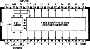
Figure 13.36 Functional diagram of the 4514B or 74HC4514 4-bit to 16-way latched decoder with active-high outputs
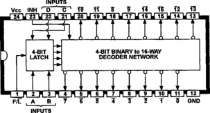
Figure 13.37 Functional diagram of the 4515B or 74HC4515 4-bit to 16-way latched decoder with active-low outputs
In these ICs, the INH control is normally held low, and when driven high disables all decoding functions; it drives all outputs low in the 4514B type, or high in the 4515B type, irrespective of the states of all other pins. Each IC acts as a direct decoder when the F/NOT-L terminal is high, but when the terminal is pulled low it latches the prevailing input code and holds it for as long as the terminal remains low; the latched code is decoded and fed to the output in the normal way.
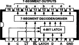
The most popular ‘4000B’-series BCD to 7-segment LED-driving IC is the 451B (also available as the 74HC4511), which has a built-in data latch and has the functional diagram shown in Figure 13.38. This IC does not incorporate ripple-blanking facilities, but is otherwise ideally suited to driving common-cathode LED displays, since its outputs can each source up to 25mA. The 4511B is very easy to use, and has only three input control terminals; of these, the NOT-LT (pin-3) pin is normally tied high, but turns on all seven segments of the display when pulled low. The NOT-BL (pin-4) terminal is also normally tied high, but blanks (turns off) all seven segments when pulled low. Finally, the LATCH (pin-5) terminal enables the IC to give either direct or latched decoding operation; when LATCH is low, the IC gives direct decoding operation, but when LATCH is taken high it holds the display in a ‘frozen’ state.
Finally, the most popular ‘4000B’-series BCD to 7-segment LCD-driving IC is the 4543B (also available as the 74HC4543), which also has a built-in data latch and has the functional diagram shown in Figure 13.39. This IC incorporates an EX-OR array (of the type shown in Figures 13.26 and 13.27) in its output driver network, which can source or sink several mA of output current.

Figure 13.39 Functional diagram of the 4543B or 74HC4543 ‘universal’ 7-segment latch/decoder/driver IC
This feature enables the IC to act as a ‘universal’ unit that can drive common-cathode or common-anode LED or liquid-crystal 7-segment displays with equal ease, as shown in Figures 13.40 and 13.41.

Figure 13.40 Way of using the 4543B (or 74HC4543) to drive (a) common-cathode or (b) common-anode 7-segment LED displays
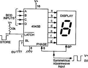
The 4543B (or 74HC4543) is delightfully easy to use. Its BL (blank) terminal is normally grounded, and blanks the entire display when pulled high, and the NOT-LATCH (pin-1) terminal gives direct decoding when biased high or latched decoding (e.g. a ‘frozen’ display) when pulled low. The IC can be used to drive a common-cathode LED display by connecting it as in Figure 13.40(a), with the PHASE control grounded, or a common-anode LED display by connecting it as in Figure 13.40(b), with the PHASE control wired to the V+ line; in both cases, resistor ‘R’ acts as a segment current-limiting resistor. The IC can be used to drive a liquid-crystal display (LCD) by connecting it as shown in Figure 13.41 and driving the IC’s PHASE and the display’s BP pins via a symmetrical squarewave that switches fully between the circuit’s supply-rail values.