Binary and Decade Counter ICs
The last chapter took a detailed look at D-type and JK flip-flops and showed how they can be used to make various simple counting/dividing circuits. The present chapter continues this theme by looking at some practical examples of modern TTL and CMOS binary and decade counter/divider ICs. The chapter starts off, however, by explaining some more counter/divider basics.
‘Count’ Direction
The design of all the multi-stage clocked flip-flop counter/dividers described in Chapter 10 is such that, in each counting sequence, each of them starts its count with all binary outputs set to the ‘0’ state, and the outputs then increment upwards on successive clock pulses until the maximum count is reached, and the whole counting process then restarts on the arrival of the next pulse. Circuits of this type are known as ‘up-counters’; all ICs described in the present chapter are up-counting types. Counter/dividers can, however, easily be designed to give a down-counting action, and a number of popular ‘down’ and ‘up/down’ counter/divider ICs are described in Chapter 12.
Synchronous or Asynchronous Counting?
In an asynchronous ripple counter, the output of one counting stage provides the clocking signal for the next stage, and as a result of each stage’s propagation delay this action may cause unwanted glitches to appear on decoded outputs as the counters switch between one set of states and another. This glitching problem does not occur with synchronous counters, which are all clocked by the same input signal; in theory, therefore, it seems that synchronous counters are technically superior to asynchronous types. In practice, however, ‘glitching’ is a purely transitory occurrence, and the only time it is of real importance is when a decoded output is used to directly drive some sort of clocked logic network, and this situation occurs in relatively few practical applications.
Thus, in most real-world applications, the synchronous counter has no practical advantage over the asynchronous type, and the design engineer should – if he/she is sure that a synchronous type is not vital for use in a particular application – simply select the most cost-effective counter IC that can be used in the circuit in question. In many cases this will be one of the several decade or binary counter/divider ICs described in this chapter. Before looking at these ICs, however, note the following points about counter ‘coding’ systems.
Counter ‘Coding’ Systems
A flip-flop counter has only two possible output states (either logic-0 or logic-1), and this number can be expressed as 2N, where N is the number of flip-flop stages and in this case equals one. This simple formula holds true for any number of cascaded flip-flop counter stages; thus, if four stages are cascaded as shown in Figure 11.1(a), in which the circuit’s four outputs are notated A, B, C and D, the maximum possible number of different ABCD ‘binary code’ output states equals 24 = 16. Note that this number of output states is only available if the counters are wired in the ripple mode; if they are connected in the Johnson mode, only eight different possible output states are available.
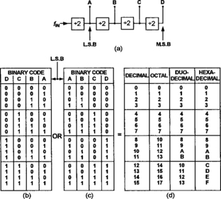
Figure 11.1 A 4-bit binary code (a) can be represented as in (b) or (c), and can be translated into any of the code systems shown in(d)
Note in the Figure 11.1(a) circuit that counter A changes state on the arrival of each new clock (fIN) pulse, and that counter D changes state on the arrival of every eighth clock pulse. Consequentially, when the ABCD code is used to represent a 4-bit binary number (such as ‘1000’, etc.) it is vital to remember that ‘A’ represents the Least Significant Bit (LSB) of that number, and ‘D’ represents its Most Significant Bit (MSB). In practice, a table of multi-bit binary codes may be written with the LSB either on the right, as in the DCBA format shown in (b), or on the left, as in the ABCD format shown in (c); neither system has any real advantage over the other, so long as it is always remembered that ‘A’ represents the code’s LSB. Similarly, when writing a binary code number such as ‘1110’ in a report, etc., it is vital to make it clear to the reader whether this is an ABCD or a DCBA code, since ‘1110’ may represent the 8th clock pulse in ABCD format or the 15th pulse in DCBA format, etc.
The tables of Figures 11.1(b) and (c) list all 16 possible 4-bit binary codes, in both DCBA and ABCD format. Each of these codes can be used, via suitable decoding/activation circuitry, to represent or perform any action or thing that you care to think of (i.e. sound an alarm, unlatch a door, display the number ‘7’, etc.). In practice, however, they are usually used to represent numbers or letters in one or other of the four standard code systems listed in table (d), in which the decimal system has a base of ten, the octal has a base of eight, the duodecimal a base of 12, and the hexadecimal (usually called ‘hex’) a base of 16.
The relevance of all this is that many popular counter ICs are internally configured to give outputs that comply with one or other of these code systems, and are supported by a variety of decoding/translating ICs. The following section describes some popular counter configurations.
Counter Configurations
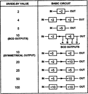
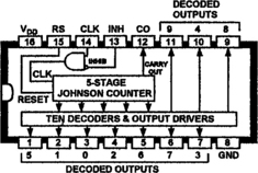
Most popular counter/divider ICs are designed to give either decade (divide-by-10) division, or some type of binary division. In the former case, the counter can be internally configured in a variety of basic ways. Figure 11.2, for example, shows (in very basic form) a synchronous decade counter made from a 5-stage Johnson counter; note that this type of counter gives a symmetrical ‘carry’ output, and that the IC incorporates decoder circuitry that provides some sort of ‘decoded’ output. The most popular IC of this type is the 4017, which provides ten fully decoded outputs; this IC is described in detail later in this chapter.

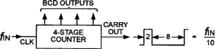
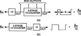
A decade counter can also take the form of a 4-stage synchronous or asynchronous counter and decoder network, configured in the basic way shown in Figure 11.3, in which the 4-bit decoded output conforms to the popular BCD (binary coded decimal) format, which can be used to drive a 7-segment LED or LCD display via a BCD-to-7-segment decoder/driver IC, or up to ten independent devices via a BCD-to-decimal decoder IC, etc. This type of counter generates an asymmetrical CARRY output with a 2:8 Mark–Space ratio.
The most popular type of decade counter configuration is that shown in Figure 11.4, in which decade division is obtained via a divide-by-2 and a divide-by-5 counter wired in series. This ‘bi-quinary’ configuration is quite versatile; the counter can be configured to generate a 4-bit BCD output and an asymmetrical ‘carry’ output by wiring it as shown in Figure 11.4(a), or as a decade divider with a symmetrical ‘carry’ output by wiring it as shown in Figure 11.4(b). One of the best known TTL ICs of this type is the 74LS90 decade divider, which is described in detail in the next section of this chapter.
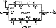
The 74LS90 IC
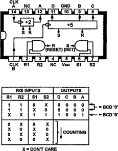
The 74LS90 is an asynchronous programmable counter/divider IC that contains independent divide-by-2 and divide-by-5 counters that are triggered by clock pulse falling edges and can be used together to give decade (divide-by-10) counting with or without BCD outputs, or can be configured to give any whole-number division value from 2 to 9 inclusive. Figure 11.5 shows the IC’s functional diagram and its R/S (RESET/SET) Truth Table. Note that the two counters share SET and RESET lines that are controlled via 2-input AND gates; normally, each of these AND gates is disabled by tying at least one terminal low; the gates are active only when both inputs (R1–R2 for RESET, S1–S2 for SET) are driven high; when RESET is active, the DCBA outputs are driven to ‘0000’ (= BCD ‘0’); when SET is active, the DCBA are driven to ‘1001’ (= BCD ‘9’); the SET control has priority over RESET.
Figures 11.6 and 11.7 show two very basic ways of using the 74LS90’s counting ability. In Figure 11.6 only the internal divide-by-2 counter is used; the divide-by-5 counter and SET/RESET gates are disabled, and the IC thus functions as a simple divide-by-2 (binary) counter. In Figure 11.7 only the internal divide-by-5 counter is used; the divide-by-2 counter and SET/RESET gates are disabled, and the IC thus acts as a simple divide-by-5 (quinary) counter.

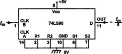
Figure 11.8 shows the IC used as a decade counter with BCD outputs. Here, both internal counters are used; fIN is fed to the input of the divide-by-2 counter, and the output (A) of this drives the input of the divide-by-5 counter; in this configuration the IC functions as a divide-by-10 counter with BCD outputs. Note that the final (pin-11) output waveform is asymmetrical, with a 2:8 Mark–Space ratio.
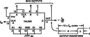
Figure 11.9 shows the IC used as a decade counter with a symmetrical (squarewave) output. Here, both internal counters are again used, but fIN is fed to the input of the divide-by-5 counter, and the output (D) of this drives the input of the divide-by-2 counter, which provides the final output; in this ‘bi-quinary’ configuration the IC thus functions as a divide-by-10 counter with a perfectly symmetrical (1:1 Mark–Space ratio) output; the outputs of this circuit are not BCD coded.

The 74LS90 can be made to divide by any whole-number value from 2 to 9 inclusive by feeding appropriate outputs back to the IC’s RESET or SET line so that the counter automatically resets each time the desired count number is reached. For divide values of 3, 4, 6 and 8 these feedback connections can be taken directly from the divide-by-5 counter’s DCB outputs; Figure 11.10 shows this counter’s Truth Table. Thus, the IC can be configured as a divide-by-3 counter by using only its divide-by-5 counter, with RESET action provided via the B and C output so that it resets to ‘000’ in the arrival of every count-3 pulse, and with the output taken from the C terminal as shown in Figure 11.11(a). The IC can be made to give divide-by-6 action by using these same basic connections, but with the input applied via the divide-by-2 counter stage, as in Figure 11.11(b). These two circuits can be modified to give divide-by-4 or divide-by-8 action by tying the R1 input to logic-1 and taking the R2 input to output D, as shown in Figures 11.12(a) and (b). For divide-by values of 7 and 9, both internal counters must be used, with the divide-by-2 counter driving the divide-by-5 counter; Figures 11.13 and 11.14 show the practical IC connections. For divide-by-7 action, both RESET terminals are grounded, but outputs B and C are coupled to the SET line via the S1 and S2 terminals, so that both counters set to the BCD-’9’ state on the arrival of the 6th clock pulse, and then reset to zero when the next (7th) clock pulse arrives. For divide-by-9 action, the counters are RESET via the A and D outputs, which both go high on the 8 + 1 count.


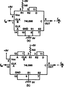

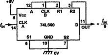
Figure 11.15 shows a practical example of a 74LS90 application circuit, in which IC1 is used to make a precision buffered-output 1MHz crystal oscillator that has its output divided down by six ripple-connected 74LS90 decade divider stages, to generate precision output frequencies of 1MHz, 100kHz, 10kHz, 1kHz, 100Hz, 10Hz, and 1Hz, which can be used as frequency or timing calibration standards, etc. Each of these 74LS90 ICs is connected in the Figure 11.9 decade divider mode and generates a symmetrical squarewave output that is very rich in odd harmonic frequencies, i.e. the 10kHz output (for example) also generates strong 30kHz, 50kHz, 70kHz, etc., output signals.

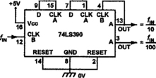
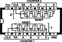
The 74LS390 IC
The 74LS390 (and its CMOS counterpart, the 74HC390) is a dual decade divider IC that can be regarded as a dual version of the basic 74LS90, but with no SET control and with greatly simplified RESET circuitry. It is cheaper than the 74LS90, and is thus a very attractive alternative to the 74LS90 in most applications where a SET facility is not needed. Figure 11.16 shows the 74LS/HC390’s functional diagram; each ‘decade’ counter is a bi-quinary type and consists of divide-by-2 and divide-by-5 counters that can be used independently but share a common RESET facility (RESET is normally grounded, and resets the decade counter to the ‘0000’ BCDA state when taken to logic-1); the divide-by-5 counter has the same Truth Table as that used in the 74LS90 (see Figure 11.10).

Note in Figure 11.16 that one decade counter appears in the lower part of the diagram, between the ‘lower’ (1 to 7) set of pin numbers, and the other is in the upper part, between the ‘upper’ (9 to 15) pin numbers; for convenience, these counters are therefore referred to in the following text by terms such as ‘upper-2’, ‘lower-5’, and ‘upper-10’, etc.
The 74LS/HC390 is a very easy IC to use. In each decade, the ‘2’ and ‘5’ counters can be used in any combination, making divide-by values of 2, 5, and 10 directly available (unwanted counters are disabled by simply grounding their CLK terminals), and each decade counter can be configured to give either a BCD or a symmetrical output. If desired, each ‘decade’ counter can alternatively be configured to give counts of 4 or 8 by connecting its RESET terminal to the C or D outputs as shown in Figure 11.17, or can be made to give counts of 3, 6, 7 or 9 by feeding various outputs back to the RESET terminal via an external 2-input AND gate as shown in Figure 11.18.
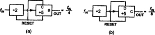
Figure 11.17 Basic ways of using a 74LS/HC390 decade divider section to give (a) divide-by-4 or (b) divide-by-8 action

Figure 11.18 Ways of using the 74LS/HC390’s decade dividers and an external 2-input AND gate to give divide-by values of (a) 3, (b) 6, (c) 7, or (d) 9
A very large total number of divide-by combinations are thus available from the 74LS/HC390 IC; Figure 11.19 shows how values of 2, 4, 5, 10, 20, 25, 50, and 100 can be obtained by just ripple-wiring the ICs standard ‘2’ and ‘5’ counters. It would be tedious to draw up a full set of wiring diagrams for all of these divide-by combinations, but Figure 11.20 shows how a divide-by-50 counter can be made by ripple-wiring the upper-5, lower-2, and lower-5 counters and disabling upper-2, and Figure 11.21 shows a divide-by-100 counter with symmetrical outputs made by ripple-wiring the upper-5, upper-2, lower-5, and lower-2 counters. In practice this versatile IC can, by using ANDed RESET control where necessary, be configured to give any desired whole-number divide-by value in the range 2 to 100 inclusive.
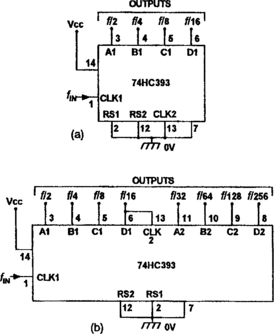
The 74HC393 Dual Binary Divider IC
The 74HC393 is a fast CMOS version of the 74LS393 Dual counter IC, and is regarded as a ‘binary’ brother of the 74HC390. Figure 11.22 shows the functional diagram of the 74HC393, which is actually a Dual 4-bit ripple counter in which each 4-bit counter has its own CLK and RESET (RS) input pins and triggers on the falling edge of its CLK signal; the RESET line sets all four outputs (A, B, C, D) into the ‘0’ state when the RS input is high, but gives normal ripple-count operation when RS is low. Thus, each counter can be used to give direct division by 2, 4, 8 or 16, or can be used to divide by any other number in the range 3 to 15 by suitably ANDing various outputs and feeding them back to the RESET line in a manner similar to that already shown in Figure 11.18.
The 74HC393’s two sets of counters can be used either independently, or can be wired in series to make an 8-bit counter that can give direct division by 2, 4, 8, 16, 32, 64, 128, or 256. Figure 11.23(a) shows how to use the IC as a 1- to 4-bit ripple counter, with the ‘1’ counter in use and the ‘2’ counter disabled, and (b) shows how to use it as a 1- to 8-bit counter, with both counters in use.
The 4017 Decade Counter IC
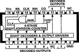
The 4017B and its ‘74HC’-series counterpart, the 74HC4017, is probably the most popular and useful of all CMOS decade counter/divider ICs. It is actually a 5-stage Johnson decade counter that has ten fully decoded outputs that sequentially switch high on the arrival of each new clock pulse, only one output being high at any moment; each output can provide several milliamps of drive current to an external load. Figure 11.24 shows the functional diagram, that applies to both versions of the IC, which has clock, reset (RS), and inhibit (INH) input terminals and ten decoded and one carry (CO) output terminals.
The main differences between the two versions of the IC are that the 4017B can use any supply in the 3V to 15V range and can operate at a maximum frequency of about 12MHz when powered from a 10V supply, while the 74HC4017 is designed to use a nominal 5V supply (actually 2V to 6V) and can operate at up to 50MHz. Bearing in mind these basic differences, note that the following text and diagrams, apply specifically to the 74HC4017 version of the device.
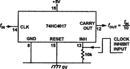
In normal use, the 74HC4017 is connected in the basic ‘decade divider’ mode shown in Figure 11.25, with its RESET and INH terminals grounded. In this mode the IC’s Johnson counter stages advance one step on the arrival of each new clock pulse rising edge and simultaneously set one of the ten decoded outputs high while the other nine outputs remain low; the outputs go high sequentially, in phase with the clock signal, with the selected output remaining high for one full clock cycle, as shown in the waveform diagram of Figure 11.26. An additional carry out (CO) signal completes one cycle for every ten clock input cycles, and can be used to ripple-clock additional 74HC4017s in multi-decade counters. Note that this IC has buffer-style inputs that are not of the Schmitt type, and the IC is thus sensitive to clock waveform shapes; the clock pulses must switch fully between normal logic levels, rise and fall times must be less than 400ns, and clock pulse widths must be greater than 15ns.
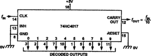
Figure 11.25 Basic connections for using the 74HC4017 as a rising-edge triggered synchronous decade divider
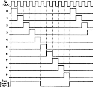
Figure 11.26 Waveform timing diagram of the Figure 11.25 circuit
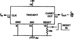
Figures 11.27 and 11.28 show two useful variations of the basic ‘decade divider’ circuit. Figure 11.27 shows how to use the IC’s pin-15 RESET control; normally this control is tied to logic-0, but when it is taken to logic-1 it resets all of the IC’s counters and sets all decoded outputs except output ‘0’ to the logic-0 state. Figure 11.28 shows the basic way of using the pin-13 clock inhibit (INH) terminal; normally, this terminal is tied to logic-0, but when it is taken to logic-1 it fully inhibits the IC’s clocking and counting actions.
There are sometimes minor architectural differences between different manufacturers’ versions of the 74HC4017, and in the Philips/Mullard version these enable the device to be triggered by the rising edges of clock signals by using the connections shown in Figure 11.25, or by falling edges by using the connections of Figure 11.29, in which the CLK (pin-14) terminal is tied to logic-1 and the clock signal is fed to the INH (pin-13) terminal (in practice, this configuration works well with most versions of the 74HC4017).
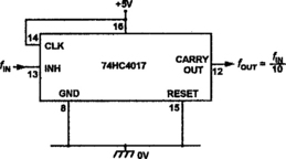
Figure 11.29 Basic way of using the Philips 74HC4017 to give falling-edge clock triggering (see text)
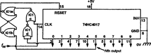
Figures 11.30 and 11.31 show ways of using the 74HC4017 as a divide-by-N counter with N decoded outputs, in which N = any whole number from 2 to 9. In the Figure 11.30 circuit the Nth decoded output is simply shorted to the reset terminal so that the counter resets to zero on the arrival of the Nth clock pulse. This circuit is slightly sensitive to the clock signal’s pulse width and rise time; the Figure 11.31 version of the counter does not suffer from this problem. Here, logic gates control the reset operation via the IC1a–IC1b flip-flop, and the action is such that the reset command is given on the arrival of the Nth clock pulse and is maintained while the clock pulse remains high, but is removed automatically when the clock pulse goes low again. Note in both diagrams that the circuit is shown set for divide-by-5 operation; also note that the IC’s ‘carry out’ terminal is effectively disabled when N values of less than 5 are used (‘carry’ signals can, however, easily be derived from the decoded ‘0’ or N outputs).

Figure 11.30 Simple way of using the 74HC4017 as a divide-by-N (2 to 9) counter; circuit is shown set for divide-by-5 operation
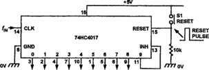
One of the 74HC4017’s most important features is its provision of ten fully decoded outputs, making the IC ideal for use in a whole range of ‘sequencing’ operations in which the outputs are used to drive LED displays, relays, or sound generators, etc. Figure 11.32 shows how it can be connected to give ‘sequence-and-stop’ operation, in which the IC stops clocking after completing a predetermined counting sequence. In the diagram the counter is set to stop when its INH terminal is driven high by the ‘9’ output, but it can in fact be inhibited via any one of the IC’s decoded output terminals. The count sequence can be restarted by pressing reset button S1, or by feeding a positive pulse to the RESET pin.
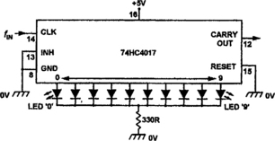
The 74HC4017 can be used as a sequencing LED display driver, operating in the ‘moving dot’ or ‘chaser’ mode (in which only one LED is illuminated at any given moment), by using the basic connections shown in Figure 11.33, in which the IC is shown used in the divide-by-10 mode; note here that the LEDs share a common current-limiting resistor, which with the value shown limits their ON currents to about 10mA.
In applications where far more than ten LEDs need to be driven in the sequential moving-dot mode, one option is to use two 74HC4017 ICs in the basic way shown in the ‘multiplexed’ circuit of Figure 11.34, which can sequentially step-drive as many as one hundred LEDs. Here, the divide-by-10 CARRY OUT signal of IC1 is fed to the CLK input of IC2, and the LEDs are connected in banks of ten with their anodes driven by IC1 and their cathodes taken to ground via switching transistors that are activated by the outputs of IC2. The circuit’s basic action is such that, for any given LED to be driven on, the appropriate outputs of both IC1 and IC2 must be high; LED12, for example, turns on only when outputs ‘2’ of IC1 and ‘1’ of IC2 are high, and so on. Thus, LEDs 0 to 9 are activated sequentially during clock pulses 0 to 9, and LEDs 10 to 19 are activated during pulses 10 to 19, and so on, right up to clock pulse 99, after which the whole sequence starts to repeat.
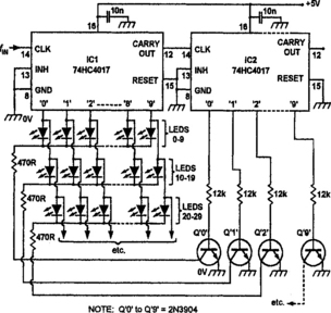
If desired, the Figure 11.34 circuit can be made to sequence repeatedly after a count of N (rather than ‘99’) by ANDing the appropriate outputs of IC1 and IC2 and feeding the ANDed signal directly to each IC’s RESET (pin-15) terminal, which must have its ground connection removed. Thus, for an N value of 27, outputs ‘2’ of IC2 and ‘7’ of IC1 must be ANDed, and the circuit needs only 27 LEDs and three switching transistors. Note that the 470R resistor connected in series with the collector of each transistor acts as an LED current limiter, and can be reduced to 220R if preferred.
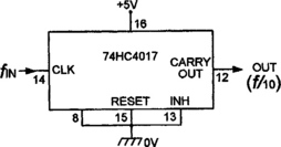
Finally, note that the 74HC4017 is sufficiently inexpensive to justify its use as a simple decade divider, in which case it should be connected as shown in Figure 11.35, with the RESET and INHIBIT terminals grounded and the output taken from the CARRY OUT terminal. Figure 11.36 shows how three decade dividers of this type can be ripple-wired (cascaded) to make a 3-decade divider that generates outputs at 1/10th, 1/100th and 1/1000th of the clock frequency; the CARRY OUT signal of each counter provides the CLOCK signal to the following stage. Note in this particular circuit that the four outputs are buffered via simple CMOS inverters to ensure that output loading does not degrade the clock signal rise times. Thus, if the clock input signal is derived from a 1MHz crystal oscillator, the circuit can be used as a laboratory frequency standard, generating frequencies of 1MHz, 100kHz, 10kHz and 1kHz.

The 4022B Octal Counter IC
The 4022B can be regarded as an octal (divide-by-8) brother of the ‘4017’. It is a synchronous 4-stage Johnson counter with eight fully decoded outputs, so arranged that they go high sequentially. Figure 11.37 shows the IC’s functional diagram. For normal octal counting, the RESET and INHIBIT terminals are tied low; the CARRY OUT signal completes one cycle for every eight input clock cycles.
Synchronous ‘UP’ Counter ICs
Synchronous ‘UP’ counters are normally used in fairly simple applications in which it is necessary merely to count a number of input pulses, or divide them by a fixed ratio, and (perhaps) then display the results on a 7-segment LED or LCD readout unit.
The 4017 and 4022 types of IC are popular examples of synchronous CMOS counter ICs; two other basic families of this type are also readily available, however. The oldest of these families consists of the 4026B and 4033B ICs, which are decade counters with built-in decoders that give 7-segment display outputs that can directly drive sensitive LED displays. The second family of devices are the 4518B and 4520B ‘Duals’, which each house two counters in a 16-pin package; the 4518B is a Dual decade counter with BCD outputs, and the 4520B is a Dual hexadecimal (divide-by-16) counter with a 4-bit binary output; the outputs of these two ICs must be decoded externally if they are to be used to drive 7-segment displays, etc. Both of these IC families are described in detail in the final two sections of this chapter.
The 4026B and 4033B Counter ICs
The 4026B and the 4033B are synchronous decade ‘UP’ counters that incorporate decoding circuitry that gives a 7-segment output suitable for directly driving a sensitive 7-segment common-cathode LED display; the output drive currents are limited to only a few mA. Both ICs have CLOCK, CLOCK INHIBIT and RESET input terminals, and a CARRY OUT output terminal that completes one cycle for every ten input clock cycles and can be used to clock following decades in a counting chain. The counters are advanced on the positive transition of the input clock cycle.
Figure 11.38 shows the outline and functional diagram of the 4026B. This IC features DISPLAY ENABLE input and output terminals, which enable the entire display to be blanked. Normally, the DISPLAY ENABLE IN pin is held high; the display blanks (but the IC continues to count) when this pin is pulled low. The IC also has an UNGATED ‘C’ SEGMENT output terminal (pin-14), which can be used with external logic to make the IC count by numbers other than ten.

Figure 11.38 Functional diagram of the 4026B decade counter with 7-segment display driver and display enable control
Figure 11.39 shows the outline and functional diagram of the 4033B. This IC features RIPPLE BLANKING input and output terminals, which can be used to automatically blank leading and trailing zeros in multi-decade applications; the ‘0’ display blanks automatically when the RIPPLE BLANKING INPUT pin is held low. The IC also features a LAMP TEST pin, which is normally held low but which drives all seven decoded outputs high when the input pin is taken high.
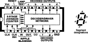
Figure 11.39 Functional diagram of the 4033B decade counter with 7-segment display driver and ripple-blanking facility
Figure 11.40 shows how to connect the 4026B and the 4033B for simple decade counter/display operation. In both cases the RESET and CLOCK INHIBIT terminals are tied low. In the case of the 4026B, the DISPLAY ENABLE INPUT must be tied high if the display is to be illuminated. In the case of the 4033B, the RIPPLE BLANKING INPUT terminal must be tied high if the display is required to give normal operation, or must be tied low if it is required to give ‘zero’ suppression. Note in both circuits that, if multi-decade counting is to be used, the CARRY OUT of one stage must be used to provide the CLOCK input signal of the next stage.
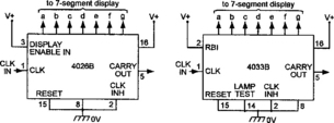
Figure 11.40 Method of connecting the 4026B and 4033B for normal decade dividing/display operation. In the case of the 4033B, the RBI connection does not give suppression of display zeros
Figure 11.41 shows how to interconnect several 4033Bs to give automatic suppression of leading and trailing zeros so that, for example, the count 009.90 is actually displayed as 9.9. To get leading zero suppression (on the integer side) the RBI (pin-3) terminal of the most significant digit (MSD) counter must be tied low, and its RBO (pin-4) terminal must be taken to the RBI terminal of the next MSD counter, and so on down to the UNITS counter. To get trailing zero suppression (on the fraction side of the display) the RBI of the least significant digit (LSD) must be tied low, and its RBO terminal must be taken to the RBI terminal of the next LSD counter, and so on, to the first counter in the ‘fractions’ chain.

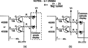
When contemplating use of the 4026B or the 4033B, note that these ICs do not incorporate DATA latches; consequently, the displays tend to ‘blur’ when the ICs are actually going through a counting cycle. Also note that the ICs have very limited output drive current capability, and produce fairly dim LED displays; if desired, the LED display brightness can be greatly increased by wiring a current-boosting transistor in series with each segment-driving output terminal, as shown in Figure 11.42.
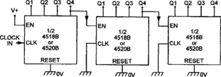
The 4518B and 4520B Counter ICs
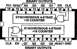
The 4518B and 4520B are Dual synchronous ‘UP’ counters with 4-bit coded outputs. The 4518B is a Dual decade counter with BCD outputs, and the 4520B is a Dual hexadecimal (divide-by-16) counter with 4-bit binary outputs. The ICs have similar functional diagrams, as shown in Figures 11.43 and 11.44.
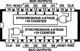
An unusual feature of these counters is that they can be clocked on either the positive (rising) or the negative (falling) edge of the clock signal. For positive-edge clocking, feed the clock to the CLK terminal and tie the ENABLE terminal high. For negative-edge clocking, feed the clock to the ENABLE terminal and tie the CLK terminal low. The counters are cleared by a high level on their RESET pins, and clear asynchronously.
Note that these counters do not have a ‘carry’ output; to cascade (ripple clock) counter stages, the negative-edge clocking feature must be utilized, as shown in Figure 11.45. Here, the Q4 output of each counter is fed to the ENABLE input of the following stage, which must have its CLK terminal tied low.