Clocked Flip-flops
Most digital ICs are based on either simple logic gate networks of the types described in earlier chapters, or on clocked bistable or flip-flop elements. This second type includes simple counter/divider ICs, shift registers, data latches, and complex ICs such as presettable up/down counters and dividers. The present chapter explains how clocked flip-flop circuits work, and presents practical user information on some popular clocked flip-flop and counter/divider ICs. As an immediate follow-up, Chapters 11 and 12 look at advanced counter/divider ICs and various associated devices.
Clocked Flip-flop Basics
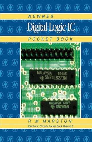
The simplest type of flip-flop is the cross-coupled bistable, which has already been briefly described in Chapter 8 (see Figures 8.7 to 8.17 Figure 8.7 Figure 8.8 Figure 8.9 Figure 8.10 Figure 8.11 Figure 8.12 Figure 8.13 Figure 8.14 Figure 8.15 Figure 8.16 Figure 8.17). Figure 10.1 shows the basic circuit, symbol and Truth Table of a NOR-gate version of this flip-flop, which has two input terminals and a pair of anti-phase output terminals (Q and NOT-Q). The circuit’s basic action is such that its Q output latches high (and NOT-Q latches low) when the SET terminal is briefly driven high (to logic-1), and remains in that state until the RESET terminal is briefly driven high, at which point the Q output latches low (and the NOT-Q output latches high). The basic SET-RESET (S–R, or R–S) flip-flop thus acts as a simple memory element that ‘remembers’ which of the two inputs last went high. Note that if both inputs go high simultaneously, both outputs go low, but if both inputs then simultaneously switch low the output states cannot be predicted; the ‘both inputs high’ condition is thus regarded as a disallowed state.

The NAND version of the S–R flip-flop (see Figure 8.11) is similar to the NOR type, except that it is triggered by logic-0 inputs. Note at this point that the S–R flip-flop is actually a Schmitt-like voltage-triggered regenerative switch; the NOR type triggers when its input (SET or RESET) voltage rises to some intermediate value (between logic-0 and logic-1) at which the CMOS element is biased into its linear amplifying mode; a NAND type triggers when the input falls to some intermediate value. Thus, all NOR-type flip-flops are intrinsically ‘level-sensitive, rising-edge-triggered’ elements, and NAND-type flip-flops are intrinsically ‘level-sensitive, falling-edge-triggered’ elements; these basic expressions form part of modern flip-flop jargon.
The versatility of the basic Figure 10.1 circuit can be greatly enhanced by wiring an AND gate in series with each input terminal, using the connections shown in Figure 10.2, so that high input signals can only reach the S–R flip-flop when the clock (CLK) signal is also high. Thus, when the clock signal is low, both inputs of the S–R flip-flop are held low, irrespective of the states of the SET and RESET inputs, and the flip-flop acts as a permanent memory, but when the clock signal is high the circuit acts as a standard R–S flip-flop. Consequently, information is not automatically latched into the flip-flop, but must be clocked in via the CLK terminal: this circuit is thus known as a ‘clocked S–R (or R–S) flip-flop’.
The master–slave Flip-flop
The most important of all basic flop-flop elements is the so-called ‘clocked master–slave’ type, and Figure 10.3 shows how one of these can be made from two cascaded S–R flip-flops that are clocked in anti-phase (via an inverter in the clock line). The basic action of this circuit is such that, when the CLK input terminal is low, the inputs to the master flip-flop are enabled via the inverter, so the SET-RESET data is accepted, but the inputs to the slave flip-flop are disabled, so this data is not passed to the output terminals. When the CLK input terminal goes high, however, the inputs to the master flip-flop are disabled via the inverter, which thus outputs only the remembered input data, and simultaneously the input to the slave flip-flop is enabled and the remembered data is latched and passed to the output terminals.

Thus, the clocked master–slave flip-flop accepts input data or information only when the clock signal is low, and passes that data to the output on the arrival of the rising edge of the clock signal, i.e. its data-shifting action is synchronous with the timing of the clock signal. The clocked master–slave flip-flop is such an important device that it is given its own circuit symbol, as shown in the diagram.
The clocked master–slave flip-flop can be made to give a divide-by-2 ‘toggle’ action by cross-coupling its input and output terminals as shown in Figure 10.4, so that SET and Q (and RESET and NOT-Q) logic levels are always opposite. Consequently, when the clock signal is low the master flip-flop receives the instruction ‘change state’, and when the clock goes high the slave flip-flop executes the instruction, so the output changes state on the arrival of the leading edge of each new clock pulse, and two clock pulses are needed to complete a full switching cycle; the output switching frequency is thus half that of the clock frequency, and this circuit, which is known as a ‘toggle’ or ‘T-type’ flip-flop, thus acts as a binary divide-by-2 counter.

Figure 10.4 A clocked ‘toggle’ or ‘T-type’ flip-flop is constructed as shown in (a), and uses the standard symbol of (b)
Figure 7.4(b) shows the basic circuit symbol of the clocked T-type flip-flop; note that the sharp-edged ‘notch’ symbol on the CLK input indicates that the flip-flop is triggered by the rising edge of a clock signal (falling-edge triggering can be notated by adding a ‘little circle’ symbol to the CLK line).
D and JK Flip-flops
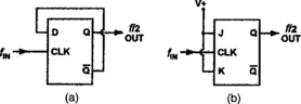
The T-type flip-flop acts purely as a counter/divider. A far more versatile device is the ‘data’ or D-type flip-flop, which is made by connecting the clocked master–slave flip-flop as shown in Figure 10.5. Here, the inverter wired between the flip-flop’s S and R terminals ensures that the signal on the DATA input is applied to these pins in anti-phase. Figures 10.5(b) and 10.5(c) show the symbol and Truth Table of the D-type flip-flop, which can be used as a data latch by using the connections shown in Figure 10.6(a), or as a binary counter/divider by using the connections shown in Figure 10.6(b) (with the D and NOT-Q terminals coupled together).


Figure 10.6 A D-type flip-flop can be used as (a) a data latch or (b) as a divide-by-2 (binary counter/divider) circuit
Figure 10.7 shows the basic circuit, symbol and action table of an even more important and versatile clocked flip-flop, which is universally known as the JK-type flip-flop. This flip-flop can be ‘programmed’ to act as either a data latch, a counter/divider, or as a do-nothing element by suitably connecting the J and K terminals as indicated in the table. In essence, the JK flip-flop acts like a T-type when both J and K terminals are high, or as a D-type when the J and K terminals are at different logic levels. When both J and K terminals are low the flip-flop states remain unchanged on the arrival of a clock pulse.

Practical TTL Flip-flop ICs
One of the best known TTL flip-flop ICs is the 74LS74. This ‘Dual’ IC houses two independent D-type flip-flops that share common power supply connections; Figure 10.8 shows the IC’s functional diagram and Truth Tables. Before looking at ways of using this IC, it is worth spending a few moments considering the general symbology, etc., used in this and other flip-flop diagrams, as follows.

Note in functional diagram (a) of Figure 10.8 that each flip-flop element has inputs that are internally notated PR and CLR, and that the feed-ins to these points carry little negation circles, indicating that PR and CLR are active-low; consequently, the actual IC pins that connect to these points should correctly be notated PR and CLR (NOT-PR and NOT-CLR) to indicate their active-low actions. The terms PR and CLR are actually abbreviations for PRESET and CLEAR, and are favoured by most manufacturers of flip-flop ICs, but – as is shown in Truth Table (c) – they give the same direct control of the Q and NOT-Q output states as conventional SET and RESET signals, and these latter terms are preferred by a few manufacturers.
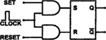
Figure 10.9 shows four common variations of the 74LS74 D-type flip-flop symbol. The (a) diagram states that the flip-flop uses rising-edge clocking and negated PR and CLR control, etc., and is an excellent ‘data sheet’ diagram; but all D-type flip-flops are edge-triggered, and the PR and CLR notations are a bit ambiguous, so the diagram of (b) is equally good. The (a) and (b) symbols are both too complex for general circuit-diagram use, and can be simplified by eliminating their negation circles, etc., and abbreviatiating and perhaps repositioning their PRESET/CLEAR or SET/RESET titles, as shown in the examples of (c) and (d).
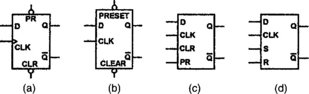
Turning now to ways of using the 74LS74 or similar D-type flip-flop elements, note from Figure 10.8‘s Truth Table (c) that ![]() and
and ![]() must be tied to logic-1 to give normal clocked operation, and from Truth Table (b) that the element can be used as a Data latch by feeding Data to the D terminal, or as a divide-by-two counter by shorting the D and NOT-Q terminals together. Figure 10.10 shows the 74LS74 connections used in these two modes of operation; in the Data latch (a) mode the ‘D’ logic-level is latched into the flip-flop and presented at its Q output by the rising edge of a clock pulse, and is then retained until another clock pulse arrives.
must be tied to logic-1 to give normal clocked operation, and from Truth Table (b) that the element can be used as a Data latch by feeding Data to the D terminal, or as a divide-by-two counter by shorting the D and NOT-Q terminals together. Figure 10.10 shows the 74LS74 connections used in these two modes of operation; in the Data latch (a) mode the ‘D’ logic-level is latched into the flip-flop and presented at its Q output by the rising edge of a clock pulse, and is then retained until another clock pulse arrives.
Figure 10.10 A Data latch (a) and a divide-by-2 counter (b) made from a 74LS74 or similar D-type flip-flop
Another popular TTL Dual flip-flop IC is the 74LS73, which has the functional diagram and Truth Tables shown in Figure 10.11. Note this IC’s unusual supply-pin connections, with pin-4 acting as Vcc and pin-11 as GND. Also note that, like most TTL JK flip-flops, it uses negative-edge triggering, as indicated by the little negation circle on the clock input of each flip-flop symbol. Each flip-flop has a negated CLR (CLEAR) terminal, which is normally biased to logic-1; when CLR is pulled to logic-0 it sets the Q output to logic-0. Figure 10.12 shows three variations of the 74LS73 JK flip-flop symbol; (a) is a strictly correct ‘Data Sheet’ type of symbol, and (b) and (c) are simplified versions suitable for use in circuit diagrams, etc.


Figure 10.12 Strictly correct (a) and common variations (b) and (c) of the 74LS73 JK flip-flop symbol
Figure 10.13 shows two basic ways of using a 74LS73 JK flip-flop element. It can be used as a divide-by-2 circuit by tying its CLR and J and K terminals to logic-1 via a shared bias resistor and feeding the input signal to the CLK terminal, as shown in (a), or as a Data latch by biasing CLR to logic-1, feeding the Data in direct form to J and inverted form to K, and using a negative-going pulse to latch the data in, as shown in (b) (note that the Standard ‘7473’ version of this IC differs slightly, and is triggered by the falling edge of a positive pulse).
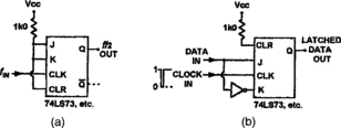
Figure 10.13 A divide-by-2 circuit (a) and a Data latch (b) made from a 74LS73 or similar JK flip-flop
There are two useful variations of the basic 74LS73 IC. One of these is the 74LS107, which is internally identical to the 74LS73 but has more conventional pin allocations, with pin-7 acting as GND, and pin-14 as Vcc; Figure 10.14 shows this IC’s functional diagram, etc. The other variation is the 74LS76, which uses a 16-pin IC package in which each flip-flop is provided with a negated PRESET (PR) terminal as well as a CLEAR (CLR) one; Figure 10.15 shows the functional diagram of this IC.


High on the list of other popular TTL flip-flop ICs are the 74LS175 Quad D-type, the 74LS273 Octal D-type, and the 74LS374 Octal D-type. In each of these ICs, all flip-flops are effectively connected in parallel and share common CLOCK and RESET (or CLR) inputs.
Practical 74HC-series Flip-flop ICs
The best-known ‘74HC’-series clocked flip-flop IC is the 74HC74 Dual D-type, which is simply a fast CMOS version of the popular 7474 or 74LS74 TTL types, and uses the functional diagram, etc., already shown in Figure 10.8. Figure 10.16 shows the connections for using a 74HC74 flip-flop element as a data latch or a divide-by-2 counter; in both cases, the CLR and PR (i.e. S and R) terminals are tied directly to the IC’s positive supply rail.

Figure 10.16 A Data latch (a) and a divide-by-2 counter (b) made from a 74HC74 (or similar) D-type flip-flop
High on the list of other popular ‘74HC’-series flip-flop ICs are the 74HC175 Quad D-type, which is simply a fast CMOS version of the 74LS175 TTL IC, and the 74HC273 and 74HC374 Octal D-types, which are simply fast CMOS versions of the 74LS273 and 74LS374 TTL ICs.
Practical ‘4000’-series Flip-flop ICs
The two best-known ‘4000’-series CMOS clocked flip-flop ICs are the 4013B D-type and the 4027B JK-type. Both of these ICs are Duals, each containing two independent flip-flops sharing common power supply connections. Figure 10.17 shows the functional diagram and Truth Tables of the 4013B, and Figure 10.18 shows similar details of the 4027B.


Note that both of these ICs have SET and RESET input terminals that are additional to the connections shown in the basic Figure 10.5 and 10.7 circuits. These terminals are known as direct inputs and enable the clock action of the flip-flop to be over-ridden, so that the devices can act as simple unclocked SET-RESET flip-flops. For normal clocked operation as a counter/divider or data latch, etc., the direct R and S terminals must be tied to logic-0, as indicated in the two sets of Truth Tables, and as shown in Figure 10.19, which shows the flip-flops configured as divide-by-2 counter/divider elements.

Figure 10.19 Specific circuit diagrams for ‘4000’-series CMOS (a) D-type and (b) JK-type divide-by-2 stages
The 4013B and 4027B are fast-acting ICs, and when using them it is very important to note that their clock signals must be absolutely clean (noise-free and bounceless) and have rise and fall times of less than 5µS. The 4013B is particularly fussy about the shape of its input clock signals, the 4027B being rather less fussy about such matters. Both devices clock or ‘shift’ on the positive transition of the clock signal.
Circuit Diagram Symbology
It is pertinent at this moment to note a few aspects of logic symbology, as applicable to clocked flip-flops and circuit diagrams. Broadly speaking, any logic-circuit diagram can be presented in either a generalized form, using greatly simplified circuit symbols, or in a specific form, using accurate circuit symbols that apply to specific ICs. Thus, all D-type flip-flops have D and CLK input terminals and Q and NOT-Q output terminals, and all JK types have J, K and CLK inputs and Q and NOT-Q outputs, so the basic ways of using any D-type or JK-type flip-flop in the divide-by-2 mode can be presented as in the general or ‘universal’ circuit diagram of Figure 10.20. If an engineer wants to build either of these circuits from a specific IC of the appropriate type he (or she) can do so by simply looking at that IC’s Data Sheet or Truth Table to find the appropriate connections for any terminals that are not mentioned in the general diagram, and then adding that data to a ‘specific’ circuit diagram, as already shown in the examples of Figures 10.16(b) and 10.19.
Thus, ‘general’ logic-circuit diagrams are a useful way of presenting valuable design information, and can easily be translated into ‘specific’ circuit diagram form. Several ‘general’ logic-circuit diagrams are used in the remaining sections of this chapter.
Ripple Counters
The most popular application of the clocked flip-flop is as a binary counter, and the reader has already seen how individual D-type and JK-type elements can be used to give divide-by-2 action in this mode; when these circuits are clocked by a fixed-frequency waveform they give a symmetrical squarewave output at half of the clock frequency.
Numbers of basic divide-by-2 stages can be cascaded to give multiple binary division by simply clocking each new stage from the appropriate output of the preceding stage. Thus, Figure 10.21 shows (in ‘general’ form) how two D or JK stages can be cascaded to give an overall division ratio of four (22), and Figure 10.22 shows how three stages can be cascaded to give a division ratio of eight (23). Figure 10.23 shows how D-type stages can be cascaded to make a divide-by-2Ncounter, where ‘N’ is the number of counter stages. Thus, four stages give a ratio of 16 (24), five stages give 32 (25), six give 64 (26), and so on. In modern flip-flop jargon, the number of stages in a multi-stage binary divider are often referred to as its ‘bit’ size; thus, a four-stage counter may be called a ‘4-bit’ counter, or an eight-stage counter an 8-bit counter, and so on.


The multi-bit circuits in Figures 10.21 to 10.23 are known as ripple dividers (or counters), because each stage is clocked by a preceding stage (rather than directly by the input clock signal), and the clock signal thus seems to ‘ripple’ through the dividers. Inevitably, the propagation delays of the individual dividers all add together to give a summed delay at the end of the chain, and divider stages (other than the first) thus do not clock in precise synchrony with the original clock signal; such divider/counters are thus asynchronous in action.
If the multi-bit outputs of a ripple divider/counter are decoded via gate networks, the propagation delays of the asynchronous dividers can result in unwanted output ‘glitches’ (see the ‘Output decoding’ section later in this chapter), so ripple counters are best used in straightforward frequency-divider applications, where no decoding is required.
Practical Ripple Counter ICs
TTL or CMOS ‘Dual’ flip-flop ICs can be cascaded to give any desired number of ripple stages, but where more than four stages are needed it is invariably more economic to use special-purpose MSI ripple-counter ICs. Figure 10.24 shows one popular but rather expensive TTL IC of this type, the 74LS93 4-bit JK ripple counter/divider, in which the four dividers are arranged in 1-bit plus 3-bit style and share a common 2-input AND gated RESET line that puts all four outputs (A, B, C, D) into the ‘0’ state when both inputs (R1 and R2) are high, but gives normal operation when one or both inputs are low. Figure 10.25(a) shows how to use this IC as a 3-bit ripple counter, with the A stage disabled and the B–C–D stages in use, and (b) shows how to use it as a 4-bit counter, with the output of the A stage feeding into the input of the B-C-D chain.
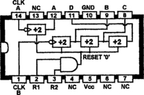
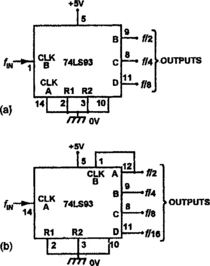
Figure 10.26 shows the functional diagram of a far more economic TTL IC, which (at the time of writing) costs half the price of the 74LS93 but has double the bit count. This is the 74LS393 Dual 4-bit ripple-counter IC, in which each 4-bit counter has its own CLOCK and RESET (RS) input pins; the RESET line puts all four outputs (A, B, C, D) into the ‘0’ state when the RS input is high, but gives normal ripple-count operation when RS is low. Figure 10.27(a) shows how to use this IC as a 1- to 4-bit ripple counter, with the ‘1’ counter in use and the ‘2’ counter disabled, and (b) shows how to use it as a 1- to 8-bit counter, with both counters in use.
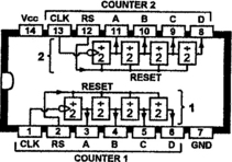
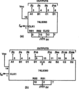
Figure 10.27 Basic ways of using the 74LS393 as (a) a 1 – to 4-bit circuit, or (b) a 1- to 8-bit circuit
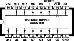
Figure 10.28 shows the functional diagram of one popular CMOS ripple counter IC, the 4024B or its ‘HC’ counterpart, the 74HC4024. This is a 7-stage ripple unit with all seven outputs externally accessible, and gives a maximum division ratio of 128. Figure 10.29 shows another popular CMOS unit, the 4040B (or 74HC4040); this is a 12-stage unit with all outputs accessible, and gives a maximum division ratio of 4096. Figure 10.30 shows the functional diagram of a 14-stage CMOS unit, the 4020B (or 74HC4020), which gives a maximum division ratio of 16,384 and has all outputs except 2 and 3 externally accessible.


Finally, Figure 10.31 gives details of another 14-stage unit, the 4060B or 74HC4060 IC. This IC does not have outputs 1, 2, 3 and 11 externally accessible, but incorporates its own built-in clock oscillator circuit. The diagram shows the connections for using the internal circuit as either a crystal or an R–C oscillator.

Figure 10.31 Functional diagram (a) of the 4060B or 74HC4060 14-stage ripple counter, with connections for using its internal gates as (b) a crystal oscillator or (c) R–C oscillator
Note that all eight of these CMOS ripple-counter ICs are provided with Schmitt-like trigger action on their input terminals, and can thus be clocked via relatively slow or non-rectangular input waveforms. They all trigger on the negative transition of each input cycle. All counters can be set to zero by applying a high level (logic-1) to the RESET line.
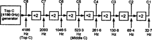
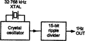
Figures 10.32 to 10.34 show three typical examples of large-bit ripple divider applications. In Figure 10.32 a ‘top-C’ (4186.0Hz) generator is used in conjunction with a 7-bit ripple divider (such as the 4024B) to make an 8-octave ‘C’ note generator that produces symmetrical outputs on terminals C1 to C7; this basic type of circuit is widely used in electronic pianos, etc. Figure 10.33 shows a 15-bit ripple divider and a 32.768kHz crystal oscillator used to make a precision 1Hz timing generator of the type that is commonly used in digital watches, and Figure 10.34 uses a 22-bit ripple divider and a commonly available 4.194304MHz crystal reference, etc., to make another precision 1Hz generator.

Output Decoding
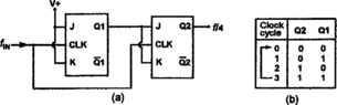
The outputs of a 2-stage divide-by-4 ripple counter have, as is shown in Figures 10.35(a) and (b), four possible binary states. Thus, at the start or ‘0’-reference point of each clock cycle the Q2 and Q1 outputs are both in the logic-0 state. On the arrival of the first clock pulse in the cycle, Q1 switches high. On the arrival of the second pulse Q2 goes high and Q1 goes low. On the third pulse Q2 and Q1 both go high. Finally, on the arrival of the fourth pulse Q2 and Q1 both go low again, and the cycle is back to its original ‘0’-reference state.

Figure 10.35 Circuit (a) and binary output states (b) of a 2-stage ripple counter Each of the four possible binary states can be decoded via a 2-input AND gate (c), but the decoded outputs may not be glitch-free, as shown in the decoded-’0’ example in (d)
Each of the four possible coded states of the ripple counter can be decoded, to give four unique outputs, by ANDing the logic-1 outputs that are unique to each one of the states, using the AND gate connections shown in Figure 10.35(c). Since the ripple counter is an asynchronous device, however, the propagation delay between the two flip-flops may cause ‘glitches’ to appear in some decoded outputs, as in the example of the decoded-’0’ waveforms shown in Figure 10.35(d).
The principles outlined in Figure 10.35 can be extended to any multi-stage ripple counter in which all significant binary outputs are accessible for decoding. Note, however, that the greater the number of stages, the greater become the total propagation delays and, consequently, the greater the magnitude (width) of any decoded glitches.
Walking-ring Counters
Ripple counters are very useful where simple binary division is needed, but (because of the ‘glitch’ problem) are not suitable for use in some sensitive decoded-counting applications. Fortunately, an alternative binary division technique is available that is well suited to the latter type of application; it is known as the ‘walking-ring’ technique. In this technique, numbers of flip-flops (usually JK types) are clocked in parallel and thus operate in synchrony with the input clock signal, and digital feedback determines how each stage will react to individual clock pulses; such counters are known as synchronous types, and they give glitch-free decoded outputs.
The JK version of the walking-ring technique depends on the fact that any JK flip-flop can be ‘programmed’ via its J and K terminals to act as either a SET or RESET latch, a binary divider, or as a do-nothing device. A detailed example of the basic walking-ring technique is given in Figure 10.36, which shows the circuit and Truth Tables of a synchronous divide-by-3 counter. Note that the Truth Table shows the action state of each flip-flop at each stage of the counting cycle, and remember that when the clock is low the action instruction is loaded (via the JK terminals) into the flip-flop, and the instruction is then carried out as the clock signal transitions high.

Thus, at the start of the cycle (CLK low), when Q2 and Q1 are both low the binary instruction ‘change state’ (11) is loaded into FF1 via its J and K terminals, and the instruction ‘set Q2 low’ (01) is loaded into FF2. On the arrival of the first clock pulse this instruction is executed, and Q1 goes high and Q2 stays low.
When the clock goes low again, new program information is fed to the flip-flops. FF1 is told to ‘change state’ (11), and FF2 is told to ‘set Q2 high’ (10), and these instructions are executed on the rising edge of the second clock pulse, causing Q2 to go high and Q1 to go low.
When the clock goes low again new program information is again fed to the flip-flops from the outputs of their partners. FF1 is instructed ‘set Q1 low’ (01) and FF2 is instructed ‘set Q2 low’ (01); these instructions are executed on the rising edge of the next clock pulse, driving Q1 and Q2 back to their original ‘0’ states. The counting sequence then repeats ad infinitum.
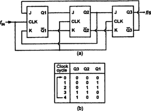
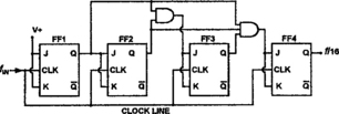
Thus, in the walking-ring counter all flip-flops are clocked in parallel, but are cross-coupled so that the clocking response of any one stage depends on the states of the other stages. Walking-ring counters can be configured to give any desired count ratio, and Figures 10.37 and 10.38 show the circuits and Truth Tables of divide-by-4 and divide-by-5 counters respectively. In some cases, circuit operation relies on cross-coupling via AND gates, etc., and an example of this is shown in the four-stage divide-by-16 counter of Figure 10.39. In walking-ring counters based on D-type flip-flops, cross-coupling may be made to the SET or RESET terminals of individual flip-flop stages, etc.
The ‘Johnson’ Counter
One useful variation of the synchronous walking-ring counter is a circuit known as the ‘Johnson’ counter, which is really a closed-loop version of a circuit known as a ‘bucket brigade’ synchronous data shifter. Figure 10.40 shows a basic bucket brigade circuit; note that it is shown built from parallel-clocked cascaded D-type flip-flops, and remember that these flip-flops latch the ‘D’-terminal data (logic state) into ‘Q’ on the arrival of the rising edge of a clock pulse. Thus, if all flip-flop outputs are initially in the logic-0 state, output A latches into the logic-1 state for one full clock cycle if a brief edge-straddling ‘start’ pulse is fed to FF1 at the start of that cycle, as shown. At the start of the next clock cycle the A waveform latches into FF2 and appears at output B, and in the next cycle it shifts down to C, and so on down the line for as many flip-flop stages as there are, until it is eventually clocked out of the circuit. Thus, the initial ‘A’ waveform passed through the circuit one step at a time, bucket-brigade style, in synchrony with the clock signal.
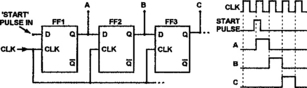
Figure 10.41 shows the basic circuit and waveforms of a 3-stage Johnson counter which is simply a bucket brigade circuit with its FF3 NOT-Q output looped back to FF1’s ‘D’ terminal. To understand the circuit operation, assume that the Q outputs of all three flip-flops are initially set at logic-0; the D input of FF1 is thus at logic-1. On the arrival of CP1 (clock pulse 1), output A latches high, and B and C remain low. On the arrival of CP2 the NOT-Q output of FF3 is still high, so output A remains in the high state, but output B is also latched high. On the arrival of CP3 the NOT-Q output of FF3 is still high, so outputs A and B remain high, but output C is also latched high. Consequently, on the arrival of CP4 the NOT-Q output of FF3 is low, so output A latches into the low state, but outputs B and C remain high. This process continues, as shown by the Figure 10.41 waveforms, until the end of CP6, and a new sequencing process then starts on the arrival of the next clock pulse.
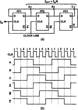
There are several important features to note about the basic Johnson counter circuit of Figure 10.41. First, note that a complete operating cycle takes six clock pulses (i.e. twice the number of flip-flop stages), and that the output waveform taken from any one of the six available output points (A, B, C, etc.) is a symmetrical squarewave with an operating frequency of fIN/6. Next, note that if the A output waveform is taken as a reference point, all other output waveforms are effectively phase-shifted by 360/6 = 60 degrees relative to A. Finally, note that the outputs of the circuit can be decoded via a 2-input AND gate to give a logic-1 output for the duration of any specific clock cycle by using the connections shown in Figure 10.42; thus, to decode CP3, simply AND outputs A and C, or to decode CP5 simply AND C and NOT-B, and so on.
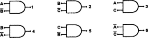
Figure 10.42 Clock-cycle decoding networks for use with the Figure 10.41 circuit
The Figure 10.41 circuit is shown built from three D-type flip-flop stages, but in practice a standard Johnson counter can be built from either D-type or JK flop-flops, can have any desired number of stages, and gives output frequency and phase shift magnitudes that are directly related to the total number of flip-flop stages. Figure 10.43 shows the basic form of the two types of circuit, together with the basic formula that is common to both circuits, and Figure 10.44 lists the basic performance details of various ‘standard’ Johnson counter circuits. Note from Figure 10.44 that the 2-stage circuit is sometimes called a ‘quadrature’ generator, since it gives four outputs that are phase-shifted by 90 degrees relative to each other, and that the 3-stage circuit (see Figure 10.41) can be used as a 3-phase (120 degree phase shift) squarewave generator by taking outputs from A, C, and NOT-B. The 5-stage circuit is widely used as a synchronous decade counter/divider (see Chapter 11).


All the Johnson counter circuits listed in Figure 10.44 give even values of frequency division (4, 6, 8, etc.), but such counters can also be made to give odd division values by varying their feedback connections, as has already been shown in the divide-by-3 and divide-by-5 examples of Figures 10.36 and 10.57. In practice, one easy way of making a circuit of this type is to use a dedicated programmable Johnson counter IC such as the 4018B.
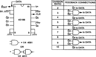
The 4018B Divide-by-N counter
Figure 10.45 shows the functional diagram and outline of the 4018B ‘presettable’ divide-by-N counter IC, which can be made to divide by any whole number between 2 and 10 by merely cross-coupling its DATA and output terminals in various ways. The 4018B incorporates a 5-stage Johnson counter, has a built-in Schmitt trigger in its clock line, and clocks on the positive transition of the input signal. The counter is said to be ‘presettable’ because its outputs can be set to a desired state at any time by feeding the inverted version of the desired binary code to the J1 to J5 ‘JAM’ inputs and then loading the data by taking the PRESET ENABLE (pin-10) terminal high.
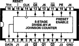
Figure 10.46 shows methods of connecting the 4018B to give any whole-number division ratio between 2 and 10. On even division ratios no additional components are needed, but on odd ratios a 2-input AND gate is needed in the feedback network.
Greater-than-10 Division
Even division ratios greater than ten can usually be obtained by simply ripple-wiring suitably scaled standard counter stages, as shown in the examples of
Figure 10.47. Thus, a divide-by-2 and a divide-by-6 stage give a ratio of 12, a divide-by-6 and divide-by-6 give a ratio of 36, and so on. Of the examples shown, the divide-by-50 and divide-by-60 counters are of particular value in converting 50Hz or 60Hz power-line frequencies into 1Hz timing signals with excellent long-term accuracy, and the multi-decade counters are of great value in generating precise decade-related signal frequencies from a single master oscillator.

Non-standard and uneven division ratios can be obtained by using standard synchronous counters (such as the 4018B) and decoding their outputs to generate suitable counter-reset pulses on completion of the desired count. More advanced types of counter, together with special decoder ICs, are described in the next two chapters.