Pulse Generator Circuits
Digital ICs must, in general, be driven or clocked by clean input waveforms that switch between normal logic levels and have very sharp leading and trailing edges; such waveforms can be generated by suitably using standard logic ICs, or via dedicated waveform-generator ICs. This chapter explains digital waveform generator basics, and shows a variety of practical pulse waveform ‘clock’ generator circuits; Chapter 9 continues the theme by taking a detailed look at practical squarewave generator circuits.
Waveform Generator Basics
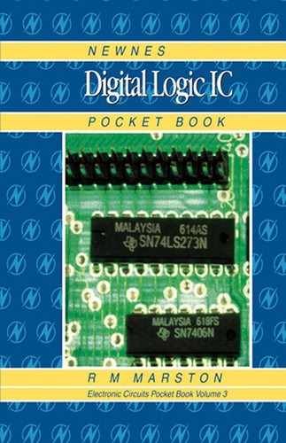
Most digital waveform generator circuits fit into one or other of the four basic categories shown in Figure 8.1(a) to (d). Schmitt trigger circuits (a) produce an output that switches abruptly between logic-0 and logic-1 values whenever an input signal goes above or below preset instantaneous voltage levels. Circuits of this type can thus be used in waveform-shaper applications, such as converting a sine or ramp input waveform into a square or pulse-shaped output, etc.
Simple bistable circuits (b) have two input terminals, known as SET and RESET. The circuit’s output can be latched into the logic-1 state by applying a suitable command signal (usually a brief logic-1 pulse) to the SET input terminal; the output can then be latched into the alternative logic-0 state only by applying a suitable command signal to the RESET terminal, and so on. ‘Latch’ circuits of this type are useful in a variety of digital signal-conditioning applications.
Monostable circuits (c) have an output that switches high on the arrival of an input trigger signal, but then automatically switches back to the low state again after some preset time delay. Circuits of this basic type thus act as triggered pulse generators.
Astable circuits (d) have an output that switches into the logic-1 state for a preset period, then switches into the logic-0 state for a second preset period, and then switches back into the first state again, and so on. Circuits of this basic type thus generate a free-running squarewave output.
In practice, all of these basic circuits can be elaborated into more complex forms. The simple monostable, for example, can be elaborated into a ‘resettable’ form, in which the output pulse can be terminated prematurely via a ‘reset’ signal, or into a ‘retriggerable’ form, in which a new monostable timing period is initiated each time a new trigger pulse arrives. Astable circuits may be completely free-running, or may be gated types which operate only in the presence of a suitable gate signal, etc.
Schmitt Edge Detector Circuits
A number of Schmitt waveform shaper, switch ‘debouncer’, and switch-on pulse-generator circuits, etc., have already been described in this book (see, for example, Figures 3.4, 3.6, 4.19, and 6.29 to 6.34). Another useful application of the Schmitt element is as an ‘edge’-detector that produces a sharp output pulse on the arrival of either the leading or the trailing edge of a digital input waveform. In most practical applications the precise width of the output pulse is non-critical.
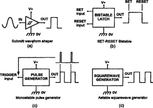
The basic way of making an edge detector is to feed the digital input waveform to a Schmitt element via a short-time-constant C–R differentiation network of the type shown on Figure 8.2, in which – when fed with a 3V squarewave input signal – the network’s output switches abruptly to +3V on the arrival of the squarewave’s rising edge but then decays rapidly to zero volts as C1 charges up via R1, and switches abruptly to −3V on the arrival of the squarewave’s falling edge but then decays rapidly to zero volts as C1 discharges via R1, and so on. In a practical Schmitt edge detector circuit, these output ‘spike’ waveforms must be fed to the Schmitt stage in such a way that only one of the two spikes has any practical effect. The Schmitt element may be of either the inverting or the non-inverting type, depending on the required polarity of the output pulse waveform; in either case, the resulting circuit is known as a half-monostable or ‘half-mono’ pulse generator.
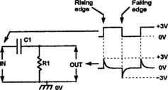
Figure 8.2 A simple C–R coupler can be used to distinguish between the ‘rising’ and ‘falling’ edges of a digital waveform
Figure 8.3(a) shows how the C–R coupler can be used in conjunction with a TTL Schmitt inverter to make a pulse-generating rising-edge detector. Here, R1 normally ties the Schmitt input low, so that its output is at logic-1, but on the arrival of the input rising edge the R1 positive spike drives the Schmitt output briefly to logic-0, so that it generates a negative-going output pulse. Note that, since the Schmitt’s input is normally tied low, the negative ‘falling edge’ input spikes have no effect on the circuit. Figure 8.3(b) shows how the circuit can be made to give a positive-going output pulse by simply taking the output via another Schmitt inverter stage.

Figure 8.4(a) shows the basic TTL Schmitt circuit modified so that it generates a positive-going output pulse on the arrival of a falling (rather than rising) input edge. Here, the Schmitt’s input is normally biased above its 1.6V upper threshold value via the R1–R2 divider, so it ignores the effects of positive ‘rising edge’ spikes, and its output is normally at logic-0. But on the arrival of each negative ‘falling edge’ spike its input is driven below the Schmitt’s 0.8V lower threshold value, and it generates a positive-going output pulse. Figure 8.4(b) shows the circuit modified to give a negative-going output pulse via an additional Schmitt inverter stage. (In practice, the output pulse widths of the Figure 8.3 and 8.4 circuits vary greatly with individual ICs, but approximate 1µs per nF of C1 value).

CMOS Schmitt elements are simpler to use than TTL types in basic edge-detector applications. This is because the built-in protection diodes that are connected to each input terminal can be used to perform the basic ‘spike discriminator’ action decribed earlier. Figure 8.5 shows two ways of making a CMOS rising edge-detecting half-mono circuit. Here, the input of the Schmitt is tied to ground via resistor R, and C–R have a time constant that is short relative to the period of the input waveform. The leading edge of the input signal is thus converted into the spike waveform shown, and this spike is then converted into a good clean pulse waveform via the Schmitt element. The circuit generates a positive-going output pulse if a non-inverting Schmitt is used (Figure 8.5(a)), or a negative-going pulse if an inverting Schmitt is used (Figure 8.5(b)); in either case, the output pulse has a period (P) of roughly 0.7CR.

Figure 8.6 shows a falling edge detecting version of the half-mono. In this case the Schmitt input is tied to the positive supply rail via R, and C–R again has a short time constant. The circuit generates a positive-going output pulse if an inverting Schmitt is used (Figure 8.6(a)), or a negative-going pulse if a non-inverting Schmitt is used. The output pulse has a period of roughly 0.7CR.
Before leaving this subject, note from Figure 8.2 that a positive-going input pulse has a rising leading edge and a falling trailing edge, so in this case a rising-edge detector acts as a ‘leading-edge’ detector, but that a negative-going input pulse has a falling leading edge and a rising trailing edge, so in this case a rising-edge detector acts as a ‘trailing-edge’ detector.
Bistable Waveform Generators
Strictly speaking, a clock generator can be any circuit that generates a clean (noiseless, with sharp leading and trailing edges) waveform suitable for clocking fast digital counter/divider circuitry, etc. One particularly useful cicuit of this type is the simple R–S (Reset–Set) bistable (also known as the R–S flip-flop), which can be used to deliver a single clock pulse each time the available one of its two input terminals is activated, either electronically or via a push-button switch, etc.
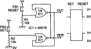
The bistable waveform generator is a circuit that can have its output set to either the logic-1 or logic-0 state by applying a suitable control signal to either its SET or RESET input terminal. The simplest way to make an S–R (or R–S) circuit of this type is to wire a pair of normal or Schmitt inverter elements into a feedback loop as shown in the TTL example of Figure 8.7. If RESET switch S1 is briefly closed it shorts the A input low, driving the A output and B input high, thus making the B output go low and lock the A input into the low state irrespective of the subsequent state of S1. The circuit thus latches into this RESET state, with its output at logic-0, until SET switch S2 is briefly closed, at which point the B output and A input are driven high, thus making the A output go low and lock the B input into the low state irrespective of the subsequent state of S2. The circuit thus latches into this SET state, with its output at logic-1, until the S1 RESET switch is next closed, at which point the whole sequence starts to repeat again.
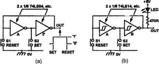
Figure 8.7 These manually-triggered TTL bistable circuits can be built from either (a) normal or (b) Schmitt inverter elements
Note that each time S1 (or S2) is operated it places a short between the B (or A) output and ground, but that the resultant output current is internally limited to safe values by the TTL inverter’s totem-pole output stage and only effectively flows for the few nanoseconds that are taken (by the circuit) to switch the inverter into its latched ‘output low’ state. These apparently brutal circuits are thus, in reality, soundly engineered and are delightfully cheap and effective designs that generate perfectly ‘bounce-free’ output switching waveforms. If desired, the circuit’s output state can be monitored by an LED connected as shown in Figure 8.7(b), so that the LED glows when the output is in the ‘RESET’ (low) state. The basic design can be modified for operation via a single toggle switch by connecting it as shown in the circuit of Figure 8.8, which generates a perfectly reliable and bounce-free ‘toggle’ output waveform.
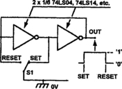
Figure 8.8 This TTL ‘bistable toggle switch’ gives perfect waveform generation from a normal toggle switch
The basic Figure 8.7 and 8.8 circuits are not really suitable for activation by electronic trigger-pulse signals, etc., but can be adapted for this operation by replacing the simple inverters with 2-input NAND or NOR gates connected as shown in Figure 8.9, so that the control inputs are not subject to odd loading effects. If NAND gates are used, both inputs must normally be biased high, and the output is SET or RESET by briefly pulling the appropriate control input low. If NOR gates are used, both inputs must normally be biased low, and the output is SET or RESET by briefly driving the appropriate input high.
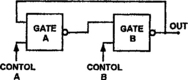
Figure 8.10 shows ways of using a TTL NAND-type SET–RESET (S–R) bistable as a manually triggered ‘toggle’ waveform generator that is activated via either (a) two push-button switches or (b) a single toggle switch. These diagrams act as handy ‘wiring’ guides, but note that the conventional way of drawing the NAND bistable is as in Figure 8.11(a). The NAND bistable is a standard logic element, and is usually called an S–R (or R–S) bistable or flip-flop; (b) shows its international circuit symbol, in which the little negation circle on each input indicates that it is activated by logic-0 levels, and which has both normal (Q) and inverted (NOT–Q) outputs; (c) shows the element’s Truth Table, which indicates that both inputs must normally be biased high (to logic-1), and that the element goes into an invalid state – with both outputs set to logic-1 – if both inputs are low at the same time. Figures 8.12 and 8.13 show practical CMOS versions of pulse-triggered and manually triggered bistables, together with their output waveforms, drawn in the ‘conventional’ manner.

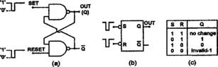
Figure 8.11 Conventional schematic (a), symbol (b), and Truth Table of the NAND-type S–R bistable or flip-flop
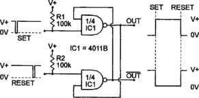

Figure 8.14 shows ways of using a TTL NOR-type S–R bistable as a manually triggered ‘toggle’ waveform generator that is activated via either (a) two push-button switches or (b) a single toggle switch. Figure 8.15(a) shows the conventional way of drawing the NOR bistable circuit, which is also a standard logic element; (b) shows the element’s international circuit symbol, and (c) shows its Truth Table, which indicates that both inputs must normally be biased low (to logic-0), and that the element goes into an invalid state – with both outputs set to logic-0 – if both inputs are high at the same time. Figures 8.16 and 8.17 show practical CMOS versions of pulse-triggered and manually triggered bistables, together with their output waveforms, drawn in the ‘conventional’ manner.
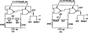
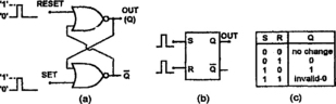
Figure 8.15 Conventional schematic (a), symbol (b), and Truth Table (c) of the NOR-type S–R (or R–S) bistable or flip-flop
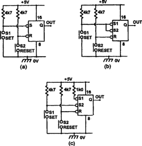
If more than two TTL S–R bistables are needed in any application, the most cost-effective way to get them is from a 74LS279 Quad S–R latch IC, which is shown in Figure 8.18, together with its Truth Table. This IC houses two normal NAND-type bistables (elements 2 and 4), plus two NAND-type bistables which each have two SET (S1 and S2) inputs. Figure 8.19 shows basic ways of using 74LS279 elements as manually triggered SET-RESET latches; (a) shows how to use a simple ‘2’ or ‘4’ element in this mode; (b) and (c) show how to use ‘2-SET’-input elements by either tying both SET terminals together, or by tying one input to logic-1 and applying the SET signal to the other.

Monostable Pulse Generator Basics
A monostable (’mono’) or ‘one-shot’ pulse generator is a circuit that generates a single high-quality output pulse of some specific width or period p on the arrival of a suitable trigger signal. In a standard monostable circuit the arrival of the trigger signal initiates an internal timing cycle which causes the monostable output to change state at the start of the timing cycle, but to revert back to its original state on completion of the cycle, as shown in Figure 8.20. Note that once a timing cycle has been initiated the standard monostable circuit is immune to the effects of subsequent trigger signals until its timing period ends naturally, but it then needs a certain ‘recovery’ time (usually equal to p or greater) to fully reset before it can again generate an accurate triggered output pulse; it thus cannot normally generate accurate pulse output waveforms with duty cycles greater than about 50%. This type of circuit is sometimes modified by adding a RESET control terminal, as shown in Figure 8.21, to enable the output pulse to be terminated or aborted at any time via a suitable command signal.
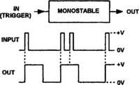
Figure 8.20 A standard monostable generates an accurate output pulse on the arrival of a suitable trigger signal

Another variation of the monostable is the ‘retriggerable’ circuit. Here, the trigger signal actually resets the mono and almost simultaneously initiates a new pulse-generating timing cycle, as shown in Figure 8.22, so that each new trigger signal initiates a new timing cycle, even if the trigger signal arrives in the midst of an existing cycle. This type of circuit has a very short recovery time, and can generate accurate pulse output waveforms with duty cycles up to almost 100%.
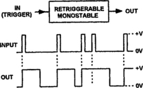
Figure 8.22 A retriggerable mono starts a new timing cycle on the arrival of each new trigger signal
Most monostables are ‘edge’ triggered, i.e. their pulse generation cycle is initiated (fired) by the arrival of the trigger signal’s rising or falling edge; this type of mono needs a well-shaped trigger signal, with fast edges. Some monostables, however, are ‘voltage level’ triggered via a Schmitt input stage, and fire when the voltage reaches a predetermined value; this type of mono can be fired by any shape of input signal.
Thus, the circuit designer may use an edge-triggered or level-triggered standard mono, resettable mono, or retriggerable mono to generate triggered output pulses, the ‘type’ decision depending on the specific circuit design requirements. In many cases, if only modest pulse-width precision is required, standard monostable circuits can be built using low-cost CMOS logic or flip-flop ICs. If greater precision or sophistication is required, the circuits can be built using one of the many TTL or CMOS dedicated pulse-generator ICs that are available.
Simple CMOS Monostable Circuits
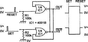
The cheapest way of making a standard or a resettable monostable pulse generator is to use a 4001B Quad 2-input NOR gate or a 4011B Quad 2-input NAND gate IC (or a ‘74HC’-series equivalent) in one of the configurations shown in Figures 8.23 to 8.26. Note, however, that the output pulse widths of these circuits are subject to fairly large variations between individual ICs and with variations in supply rail voltage, and these circuits are thus not suitable for use in high-precision applications.
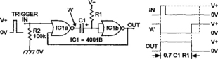
Figure 8.23 2-gate NOR monostable is triggered by a positive-going signal and generates a positive-going output pulse

Figure 8.24 2-gate NAND monostable is triggered by a negative-going signal and generates a negative-going output pulse


Figures 8.23 and 8.24 show alternative versions of the standard monostable circuit, each using only two of the four available gates in the specified CMOS package. In these circuits the duration of the output pulse is determined by the C1–R1 values, and approximates 0.7 × C1 × R1. Thus, when R1 has a value of 1M5 the pulse period approximates one second per µF of C1 value. In practice, C1 can have any value from about 100pF to a few thousand µF, and R1 can have any value from 4k7 to 10M.
An outstanding feature of these circuits is that the input trigger signal can be direct coupled and its duration has little effect on the length of the generated output pulse. The NOR version of the circuit (Figure 8.23) has a normally low output and is triggered by the edge of a positive-going input signal, and the NAND version (Figure 8.24) has a normally high output and is triggered by the edge of a negative-going input signal. Another feature is that the pulse signal appearing at point ‘A’ has a period equal to that of either the output pulse or the input trigger pulse, whichever is the greater of the two. This feature is of value when making pulse-length comparators and over-speed alarms, etc.
The operating principle of these monostable circuits is fairly simple. Look first at the case of the Figure 8.23 circuit, in which IC1a is wired as a NOR gate and IC1b is wired as an inverter. When this circuit is in the quiescent state the trigger input terminal is held low by R2, and the output of IC1b is also low. Thus, both inputs of IC1a are low, so IC1a output is forced high and C1 is discharged.
When a positive trigger signal is applied to the circuit the output of IC1a is immediately forced low and (since C1 is discharged at this moment) pulls IC1b input low and thus drives IC1b output high; IC1b output is coupled back to the IC1a input, however, and thus forces IC1a output to remain low irrespective of the prevailing state of the trigger signal. As soon as IC1a output switches low, C1 starts to charge up via R1 and, after a delay determined by the C1–R1 values, the C1 voltage rises to such a level that the output of IC1b starts to swing low, terminating the output pulse. If the trigger signal is still high at this moment, the pulse terminates non-regeneratively, but if the trigger signal is low (absent) at this moment the pulse terminates regeneratively.
The Figure 8.24 circuit operates in a manner similar to that described above, except that IC1a is wired as a NAND gate, with its trigger input terminal tied to the positive supply rail via R2, and the R1 timing resistor is taken to ground.
In the Figure 8.23 and 8.24 circuits the output is direct-coupled back to one input of IC1a to effectively maintain a ‘trigger’ input once the true trigger signal is removed, thereby giving a semi-latching circuit operation. These circuits can be modified so that they act as resettable monostables by simply providing them with a means of breaking this feedback path, as shown in Figures 8.25 and 8.26. Here, the feedback connection from IC1b output to IC1a input is made via R3. Consequently, once the circuit has been triggered and the original trigger signal has been removed each circuit can be reset by forcing the feedback input of IC1a to its normal quiescent state via push-button switch PB1. In practice, PB1 can easily be replaced by a transistor or CMOS switch, etc., enabling the RESET function to be accomplished via a suitable reset pulse.
CMOS ‘flip-flop’ Monostable Circuits
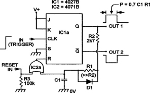
Medium-accuracy monostables can also be built by using standard edge-triggered CMOS flip-flop ICs such as the 4013B dual D-type or the 4027B dual JK-type (both of these ICs are described in detail in Chapter 10) in the configurations shown in Figures 8.27 and 8.28. Both of these circuits operate in the same basic way, with the IC wired in the frequency divider mode by suitable connection of its control terminals (DATA and SET in the 4013B, and J, K, and SET in the 4027B), but with the Q terminal connected back to RESET via a C–R time-delay network. The operating sequence of each circuit is as follows.


When the circuit is in its quiescent state its Q output pin is low and discharges timing capacitor C1 via R2 and the parallel combination D1–R1. On the arrival of a sharply rising leading edge on the clock terminal the Q output flips high, and C1 starts to charge up via the series combination R1–R2 until eventually, after a delay determined mainly by the C1–R1 values (R1 is large relative to R2), the C1 voltage rises to such a value that the flip-flop is forced to reset, driving the Q terminal low again. C1 then discharges rapidly via R2 and D1–R1, and the circuit is then ready to generate another pulse on the arrival of the next trigger signal.
The timing period of the Figure 8.27 and 8.28 circuits approximates 0.7 × C1 × R1, and the ‘reset’ period (the time taken for C1 to discharge at the end of each pulse) approximates C1 × R2. In practice, R2 is used mainly to prevent degradation of the trailing edge of the pulse waveform as C1 discharges; R2 can be reduced to zero if this degradation is acceptable. Note that the circuit generates a positive-going output pulse at Q, and a negative-going pulse (which is not influenced by the R2 value) at NOT-Q.
The Figure 8.27 and 8.28 circuits can be made resetable by connecting C1 to the RESET terminal via one input of an OR gate and using the other input of the OR gate to accept the external RESET signal. Figure 8.29 shows how the 4027B circuit can be so modified.
Finally, Figure 8.30 shows how the 4027B can be used to make a retriggerable monostable in which the pulse period restarts each time a new trigger pulse arrives. Note that the input of this circuit is normally high, and that the circuit is actually triggered on the trailing (rising) edge of a negative-going input pulse. The circuit operates as follows.
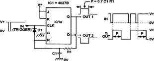
At the start of each timing cycle the input trigger pulse switches low and rapidly discharges C1 via D1 and then, a short time later, the trigger pulse switches high again, releasing C1 and simultaneously flipping the Q output high. The timing cycle then starts in the normal way, with C1 charging via R1 until the C1 voltage rises to such a level that the flip-flop resets, driving the Q output low again and slowly discharging C1 via R1. If a new trigger pulse arrives in the midst of a timing period (when Q is high and charging C1 via R1), C1 discharges rapidly via D1 on the low part of the trigger, and commences a new timing cycle as the input waveform switches high again. In practice, the input trigger pulse must be wide enough to fully discharge C1, but should be narrow relative to the width of the output pulse. The output pulse timing period equals 0.7 × C1 × R1. For best results, R1 should have as large a value as possible.
TTL Monostable IC Circuits
In TTL circuitry, the best way of generating high quality pulses is via a dedicated TTL pulse-generator IC such as the 74121, 74LS123, or 74LS221. Figure 8.31 shows the functional diagram, etc., of the 74121. This old but very popular ‘standard’ monostable pulse generator IC can give useful output pulse widths from 30nS to hundreds of mS via (usually) two external timing components, and can be configured to give either level-sensitive rising-edge or simple falling-edge triggering action. Note that the IC has three available trigger-input terminals; of these, A1 and A2 are used as falling-edge triggering inputs, and B functions as a level-sensitive Schmitt rising-edge triggering input; Figure 8.32 shows how to connect these inputs for a specific type of trigger action.


Thus, for rising-edge or voltage level triggering, A1 and A2 must be grounded and the trigger input is applied to B, as shown in Figure 8.33 (which also shows the two external timing components wired in place). For falling-edge triggering, B must be tied to logic-1, and the trigger input must be applied to A1 and/or A2, but the unused ‘A’ input (if any) must be tied to logic-1; Figure 8.34 shows an example of one of these options, with B and A2 tied to logic-1, and the trigger input applied to A1.
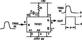
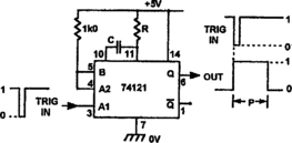
Dealing next with the 74121’s timing circuitry, this IC has three timing-component terminals. A low-value timing capacitor is built into the IC and can be augmented by external capacitors wired between pins 10 and 11 (on polarized capacitors the ‘+’ terminal must go to pin-11). The IC also incorporates a 2k0 timing resistor that is used by connecting pin-9 to pin-14 either directly or via a resistance of up to 40k; alternatively, the internal resistor can be ignored and an external resistance (1k4 to 40k) can be wired between pin-11 and pin-14. Whichever connection is used, the output pulse width = 0.7RTCT, where width is in milliseconds, RT is the total timing resistance, and CT is the timing capacitance in microfarads. Note that the circuits of Figures 8.33 and 8.34 show the normal methods of using the 74121, with external timing resistors and capacitors.
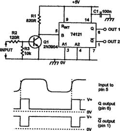
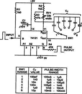
Figure 8.35 shows the 74121 used as a 30nS pulse generator, using only the IC’s internal timing components, and with its trigger signal connected to the B (Schmitt) input via a simple transistor buffer stage, and Figure 8.36 shows it used to make an add-on pulse generator that can be used with an existing squarewave ‘trigger’ generator and spans the range 100ns to 100ms in six decade ranges, using both internal and external timing resistors and decade-switched external capacitors.
One type of pulse generator widely used in laboratory work is the delayed-pulse generator, which starts to generate its output pulse at some specified delay-time after the application of the initial trigger signal. Figure 8.37(a) shows the typical waveforms of this type of generator, and (b) shows the basic way of making such a generator from two 74121 ICs. Here, the trigger input signal fires IC1, which generates a ‘delay’ pulse, and as this pulse ends its inverted (NOT-Q) output fires IC2, which generates the final (delayed) output pulse.
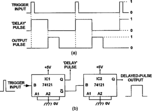
Figure 8.38 shows how two of the basic Figure 8.36 circuits can be coupled together to make a practical ‘add-on’ wide-range delayed-pulse generator in which both the ‘delay’ and ‘output pulse’ periods are fully variable from 100ns to 100ms. Note in this circuit that both fixed-amplitude inverted and non-inverted outputs are short-circuit protected via 47R series resistors. This circuit’s timing periods and CT values are identical to those listed in the table of Figure 8.36.

Figure 8.39 shows the functional diagram of the 74LS123 Dual retriggerable monostable with CLEAR, together with basic connections for its external timing components (R and C); note that pins 6 and 14 are internally connected to pin-8 (ground), and that internal capacitances of about 20pF exist between pins 6–7 and pins 14–15. In this IC, each mono has three input trigger-control terminals, notated A, B, and CLR. Normally, CLR must be biased to logic-1 (via a 1k0 resistor); it sets the Q output at logic-0 when CLR is pulled low.
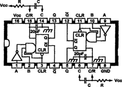
Figure 8.39 Functional diagram and basic external timing-component connections of the 74LS123 Dual retriggerable monostable with CLEAR
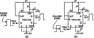
The 74LS123 can be triggered in three different modes via the A, B, and CLR terminals, as shown in Figures 8.40 and 8.41. It can be triggered in the rising-edge mode by tying A to logic-0, CLR to logic-1, and applying the trigger signal to B, as shown in Figure 8.41(a), or in the falling-edge mode by tying B and CLR to logic-1 and applying the trigger signal to A, as shown in (b). The third ‘negative-pulse rising-edge’ mode – shown in (c) – is rarely used; here, A is set to logic-0, B and CLR are biased to logic-1, and the negative-going trigger pulse is applied to CLR; the falling-edge of this pulse resets the monostable, and the rising-edge triggers a new monostable period.


Figure 8.41 Basic ways of using a 74LS123 to give (a) rising-edge, (b) falling-edge, or (c) negative-pulse rising-edge triggering
Dealing next with the 74LS123’s timing network, this consists of an external resistance (5k0 to 260k) connected between the C/R terminal and the positive supply line, and a capacitance (of any appropriate value) connected between C/R and either the ‘C’ terminal or ground; Figure 8.42 shows three alternative ways of connecting these components. The 74LS123’s timing period is given approximately by:
where ‘p’ = pulse width in nanoseconds, RT = resistance in kilohms, and CT = total capacitance (including the internal 20pF) in pF; thus, external values of 25k and 10nF give pulse widths of about 100µs, etc. Note that these values are subject to some variation between individual ICs, and with variations in supply voltage and temperature (typically up to ±1% over the IC’s voltage range, and up to −2% over its operating temperature range).

Before leaving the 74LS123, note that if only one of its monostables is needed, the unwanted monostable should be disabled by tying its CLR terminal high and grounding its A and B terminals, as shown in Figure 8.43.

Finally, Figure 8.44 shows the functional diagram of the 74LS221 Dual precision Schmitt-triggered monostable with CLEAR, together with basic connections for its external timing components (R and C); note that the external C must be connected between pins 6–7 or 14–15, and that these pins are shunted by an internal capacitance of about 5pF. Also note that the 74LS221 is NOT a retriggerable IC, and is thus subject to the normal duty-cycle limitations of an ordinary monostable; the IC should in fact be regarded as an improved high-performance Dual version of the old 74121 (at the time of writing, it costs less than half the 74121 price). In the 74LS221, each mono has three Schmitt-type input trigger-control terminals, notated A, B, and CLR, with semi-latching action on B and CLR via an internal NAND-type flip-flop (FF). Normally, CLR must be biased to logic-1 (via a 1k0 resistor); it sets the Q output at logic-0 if it is pulled low.

Figure 8.44 Functional diagram and basic external timing-component connections of the 74LS221 Dual precision Schmitt-triggered monostable with CLEAR
The 74LS221 can be triggered in three different modes via the A, B, and CLR terminals, as shown in Figures 8.45 and 8.46. It can be triggered in the rising-edge mode by tying A to logic-0, CLR to logic-1, and applying the trigger signal to B, as shown in Figure 8.46(a), or in the falling-edge mode by tying B and CLR to logic-1 and applying the trigger signal to A, as shown in (b). The third ‘negative-pulse rising-edge’ mode is rarely used; here, A is set to logic-0, and the circuit is then primed by switching B from logic-0 to logic-1 while CLR is held at logic-0; then, with B at logic-1, a rising-edge on CLR will trigger a monostable period.
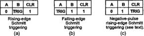
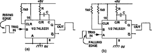
Figure 8.46 Basic ways of using a 74LS221 to give (a) rising-edge or (b) falling-edge Schmitt triggering action
Dealing next with the 74LS221’s timing network, this consists of an external resistance (1k4 to 100k) connected between the C/R terminal and the positive supply line, and a capacitance (of any value up to 1000µF) connected between C/R and the C terminal, as shown in Figure 8.46. The 74LS221’s timing period is given approximately by:
where ‘p’ = pulse width in nanoseconds, RT = resistance in kilohms, and CT = total capacitance (including the internal 5pF) in pF; thus, external values of 25k and 10nF give pulse widths of about 175µs, etc. Note that these values are virtually independent of variations in supply voltage and temperature over the IC’s full voltage/temperature operating range.
In applications where only one of the 74LS221’s monostables is needed, the unwanted monostable should be disabled by tying its CLR terminal high and grounding its A and B terminals, as shown in Figure 8.47.

‘4000’-series Monostable ICs
Several dedicated CMOS monostable ICs are readily available, and the best known ‘4000’-series versions of these are the 4047B monostable/astable IC, and the 4098B Dual monostable (a greatly improved version of the 4528B). Figures 8.48 and 8.49 show the functional diagrams of these two devices, together with the locations of their external timing components. These ICs give only moderately good pulse-width accuracy and stability, but can be triggered by either the positive or the negative edge of an input signal and can be used in either the standard or the retriggerable mode.

Figure 8.48 Functional diagram and external timing component locations of the 4047B monostable/astable IC

Figure 8.49 Functional diagram and external timing component locations of the 4098B Dual monostable IC
The 4047B houses an astable multi and a divide-by-2 stage, plus logic networks. When used in the monostable mode the trigger signal starts the astable and resets the counter, driving its Q output high; after two C–R-controlled astable cycles the counter flips over and simultaneously kills the astable and switches the Q output low, completing the operating sequence. The C–R timing components produce relatively long output pulse periods, which approximate 2.5CR (R can have any value from 10k to 10M, and C must be a non-polarized capacitor with a value greater than 1nF). Figures 8.50(a) and 8.50(b) show how to connect the IC as a standard monostable triggered by either positive (a) or negative (b) input edges, and Figure 8.50(c) shows how to connect the monostable in the retriggerable mode; these circuits can be reset at any time by pulling RESET pin-9 high.

Figure 8.50 Various ways of using the 4047B as a monostable. (a) Positive-edge-triggered monostable. (b) Negative-edge-triggered monostable. (c) Retriggerable monostable, positive-edge triggered
The 4047B can be used as a free-running astable multivibrator (squarewave generator) by connecting it as in Figure 8.51 The user has two output options in this mode. Pin-13 allows the output of the internal astable to be directly accessed; this output may not be precisely symmetrical, and has a period of 2.2CR. Alternatively, the output may be taken (from pin-10 or 11) via the internal divide-by-2 element, in which case the output is perfectly symmetrical and has a period of 4.4CR.

Figure 8.51 Basic ways of using the 4047B as a free-running astable multivibrator. (a) Direct squarewave output (may not be symmetrical). (b) Divide-by-2 outputs are perfectly symmetrical
Figure 8.52 shows various ways of using the 4098B Dual monostable IC. This is a fairly simple device, in which the two monostable sections share common supply connections but can otherwise be used independently. Mono-1 is housed on the left side (pins 1 to 7) of the IC, and mono-2 on the right side (pins 9 to 15). The timing period of each mono is controlled by a single resistor (R) and capacitor (C), and approximates 0.5CR. R can have any value from 5k0 to 10M, and C can have any value from 20pF to 100µF. Note in the diagrams of Figure 8.52 that the bracketed numbers relate to the pin connections of mono-2, and the plain numbers to mono-1, and that the RESET terminal (pins 3 or 13) is shown disabled.
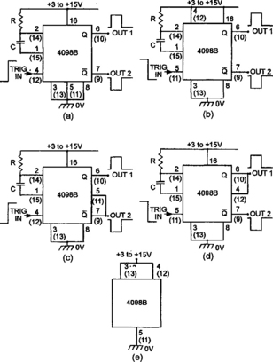
Figure 8.52 Various ways of using the 4098B monostable. (a) Positive-edge-triggering, retriggerable mono. (b) Negative-edge-triggering, retriggerable mono. (c) Positive-edge-triggering (non-retriggerable mono). (d) Negative-edge-triggering (non-retriggerable mono). (e) Connections for each unused section of the IC
Figures 8.52(a) and 8.52(b) show how to use the 4098B to make retriggerable monostables that are triggered by positive or negative input edges respectively. In Figure 8.52(a) the trigger signal is fed to the ‘+’ TRIG pin, and the ‘−’ TRIG pin is tied low. In Figure 8.52(b) the trigger signal is applied to the ‘–’ TRIG pin, and the ‘+’ TRIG pin is tied high.
Figures 8.52(c) and 8.52(d) show how to use the IC to make standard (non-retriggerable) monostables that are triggered by positive or negative edges respectively. These circuits are similar to those mentioned above except that the unused trigger pin is coupled to either the Q or the NOT-Q output, so that trigger pulses are blocked once a timing cycle has been initiated.
Finally, Figure 8.52(e) shows how the unused half of the IC must be connected when only a single monostable is wanted from the package. The ‘–’ TRIG pin is tied low, and the ‘+’ TRIG and RESET pins are tied high.
‘74HC’-series Monostable ICs
The three best known ‘74HC’-series monostable ICs are the 74HC123, 74HC221, and the 74HC4538. These are all Dual monostable types. The 74HC4538 is a Dual retriggerable mono, with CLEAR, and is functionally almost identical to the 4098B, and uses the same pin notations, etc. (see Figure 8.49); each monostable generates a pulse with a period (width) of 0.7CR.
The 74HC123 (see Figure 8.53) is a Dual retriggerable monostable, with CLEAR, and is a modified fast CMOS version (with Schmitt ‘trigger’ inputs) of the popular 74LS123 TTL IC, but its ‘C’ terminals (pins 6 and 14) are not internally connected to the GND terminal, and in use these pins must be hard-wired to GND. The IC is used in a similar way to the 74LS123 (see Figures 8.54 to 8.55), but each monostable generates an output pulse with a period of 1.0 × CR, and R can have any value up to 10M.
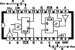
Figure 8.53 Functional diagram and external timing component locations of the 74HC123 Dual retriggerable monostable with CLEAR. Note: In use, terminal C (pins 6 and 14) must be hard-wired to GND

Finally, the 74HC221 is another Dual retriggerable monostable with CLEAR and with Schmitt ‘trigger’ inputs, and is simply a modified fast CMOS version of the popular 74LS221 TTL IC. It is, for most practical purposes, functionally similar to the 74HC123, and is used in the ways already shown in Figures 8.54 and 8.55. Like the 74HC123, its ‘C’ terminals (pins 6 and 14) are not internally connected to the GND terminal, and in use must be hard-wired to GND. Each monostable generates an output pulse with a period of 1.0 × CR, and R can have any value up to 10M.