Buffer, Gate, and Logic IC Circuits
Earlier chapters of this book explained TTL and CMOS principles and basic usage rules, and looked at the ‘74’- and ‘4000’-series of ICs and at various sub-members of these families. The present chapter carries on the ‘digital ICs’ theme by showing practical ways of using TTL and CMOS buffers, inverters, and logic gate ICs.
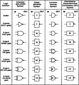
Logic Gate Symbology
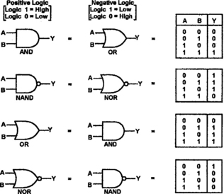
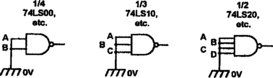
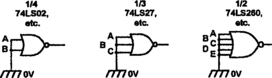
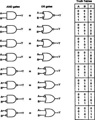
The eight best known types of logic ‘gate’ are the buffer and the NOT, OR, NOR, AND, NAND, EX-OR and EX-NOR types. Many different symbols can be used to represent each of these eight basic logic gate elements. Figure 6.1 shows four different families of symbols that are widely used in various parts of the world today; of these, the American MIL/ANSI symbols are by far the most popular, are instantly recognizable, are used by most of the world’s practical digital engineers, and are used throughout this book. Two useful variations of these American symbols are also widely used and are shown added to a standard inverter symbol in Figure 6.2; the left-hand symbol is internationally recognized and indicates that the logic element has a Schmitt-trigger input action; the right-hand symbol – which is widely used but is not universally recognized – indicates that the logic element has an open-drain (o.d.) or open-collector (o.c.) output stage.

Logic Gate Functions
The functional action of any logic gate can be described either in words or in a tabular or symbolic way. The following list describes the functions of all eight basic types of gate in words.
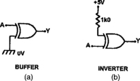
Buffers.: A buffer is a non-inverting amplifier that has an output drive capacity that is far greater than its input drive requirement, i.e. it has a high fan-out and gives a logic-1 output for a logic-1 input, etc.
Inverters.: An inverter (also known as a NOT gate) is a high fan-out amplifier that gives a logic-1 output for a logic-0 input, and vice versa.
AND gates.: An AND gate has an output that is normally at logic-0 and only goes to logic-1 when all inputs are at logic-1, i.e. when inputs A and B and C, etc. are high.
NAND gates.: A NAND gate is an AND gate with a negated (inverted) output; the output is normally at logic-1 and only goes to logic-0 when all inputs are at logic-1.
OR gates.: An OR gate has an output that goes to logic-1 if any input is at logic-1, i.e. if inputs A or B or C, etc., are high. The output goes to logic-0 only if all inputs are at logic-0.
NOR gates.: A NOR gate is an OR gate with a negated output; it has an output that goes to logic-0 if any input is at logic-1, and goes to logic-1 only when all inputs are at logic-0.
EX-OR gates.: An exclusive-OR (EX-OR) gate has two inputs, and its output goes to logic-1 only if a single input (A or B) is at logic-1; the output goes to logic-0 if both inputs are in the same logic state.
EX-NOR gates.: An exclusive-NOR (EX-NOR) gate is an EX-OR gate with a negated output, which goes to logic-1 if both inputs are in the same logic state, and goes to logic-0 only if a single input is at logic-1.
Figure 6.3 shows how the functions of the eight gates can also be presented in tabular form via Truth Tables (which show the logic state of the output at all possible input logic state combinations), or symbolically via Boolean algebraic terms (an explanation of Boolean algebra basics is given in the author’s Modern TTL Circuits Manual ). Note that, by convention, all logic gate inputs are notated alphabetically as ‘A’, ‘B’, ‘C’, etc., and the output terminal is notated as ‘Y’ (but in counters and flip-flops, etc., the main output is usually notated as ‘Q’); the actual logic states may be represented by ‘0’ and ‘1’, as shown, or by ‘L’ (= Low logic level) and ‘H’ (= High logic level). Also note in the Boolean expressions that a negated output is indicated by a negation bar drawn above the basic output symbol; the negated state is called a ‘not’ state; thus, a negated ‘Y’ output is called a ‘not-Y’ output.

Positive Versus Negative Logic
All modern digital logic circuitry assumes the use of the ‘positive logic’ convention, in which a logic-1 state is High and a logic-0 state is Low. In the early days of electronic digital circuitry an alternative ‘negative logic’ convention – in which a logic-1 state is Low and a logic-0 state is High – was also in common use, and it is sometimes still useful to be able to think in negative-logic terms, particularly when designing gates in which a Low-state output is of special interest. With this point in mind, Figure 6.4 presents a basic set of 2-input Positive and Negative logic equivalents. Thus, it can be seen that a Negative logic AND gate action – in which the output is Low only when both inputs are Low – is directly available from a Positive logic OR gate, and so on.
Practical Buffer IC Circuits
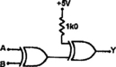
Digital buffer ICs have two main purposes, and these are to act either as simple non-inverting current-boosting interfaces between one part of a circuit and another, or to act as 3-state switching units that can be used to connect a circuit’s outputs to a load only when required. If you ever need only a few simple buffers, one cheap way to get them is to make them from spare AND or OR elements, as shown in Figure 6.5, or from pairs of normal or Schmitt inverters, as shown in Figure 6.6.
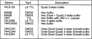
Figure 6.7 lists basic details of nine popular non-inverting buffer ICs. When using these ICs, note that all unused buffers must be disabled by tying their inputs to one of the IC’s supply lines. In CMOS devices, the unused inputs can be tied directly to either supply line, but in TTL devices it is best (for lowest quiescent current consumption) to tie all unused inputs high via a common 10k resistor; if the unused buffer is a 3-state type, it should (if it has independent control) be set into its ‘normal’ mode via its control input.
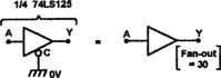
Dealing now with the individual buffer ICs listed in Figure 6.7, Figure 6.8 shows the functional diagram and Truth Table, etc., of the 74LS125 TTL IC, which houses four independently controlled 3-state buffers and is so modestly priced that it is still worth using even if you do not need the ‘3-state’ facility. Note from the Truth Table that each of the four elements acts as a normal buffer when its control terminal (C) is in the logic-0 state, and that the element’s quiescent current (Is) is least when C is at logic-0 and the buffer’s input (A) is at logic-1. Thus, any unwanted elements should be disabled by tying their C terminals Low and their A terminals High, using one of the methods shown in Figure 6.9, and any element can be used as a normal buffer by grounding its C terminal as in Figure 6.10, or as a 3-state buffer that drives a common bus line by using it as shown in Figure 6.11.
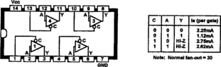
Figure 6.8 Functional diagram and Truth Table, etc., of the 74LS125 Quad 3-state buffer/bus-driver IC


If you need up to six simple CMOS buffers, one of the cheapest ways to get them is via a 4050B or 74HC4050 Hex buffer IC. Figure 6.12 shows the IC’s functional diagram; each buffer can source up to 10mA or sink up to 40mA of output current when the IC is powered from a 15V supply.

If you need up to six 3-state CMOS buffers, one option is to use a 4503B Hex buffer IC. Figure 6.13 shows the functional diagram and Truth Table of this versatile IC, in which pin-1 acts as a DISABLE input that controls four of the six buffers, and pin-15 acts as a DISABLE input that controls the other two buffers. Note that each buffer element acts as a normal buffer when its DISABLE pin is at logic-0 (low), and goes into the high-impedance output state when its DISABLE pin is at logic-1 (high). Thus, this IC can be used as a simple Hex buffer by wiring it as shown in Figure 6.14 (with pins 1 and 15 grounded), or as a Hex 3-state buffer that is controlled via a single input by wiring it as shown in Figure 6.15 (with pins 1 and 15 shorted together and used as a DISABLE input)
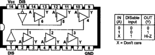
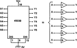

Figure 6.15 Method of connecting the 4503B for use as a 3-state Hex buffer controlled via a single input
Figure 6.16 shows the functional diagram of the 7407, which is a Standard-TTL Hex buffer in which each buffer has an open-collector (o.c.) output that can sink up to 40mA and can be connected to a supply of up to 30V via an external current-limiting pull-up resistor (but the actual IC must use a 5V supply); Figure 6.17 shows how one of these buffers can be used as a 5V to high-voltage (up to 30V) non-inverting interface. Figure 6.18 shows how three o.c. buffers can be made to act as a wired- AND gate by wiring all three outputs to the same pull-up resistor; the circuit action is such that the output is pulled low when any input is low, and only goes high when all three inputs are high, thus giving an AND action.
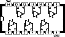


Figure 6.19 shows the functional diagram and basic Truth Table of a 74LS365 Hex 3-state buffer IC, in which all six buffers share a common AND-gated control line. This IC can be used as six normal buffers by grounding its two control pins as shown in Figure 6.20, or as a set of six 3-state buffers that are all switched via one common control signal as shown in Figure 6.21; AND-type 3-state control can be obtained by using both ‘Control’ terminals (pins 1 and 15).
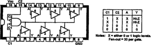
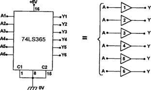
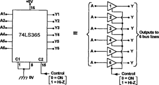
Figure 6.21 Methods of connecting the 74LS365 for use as a 3-state Hex buffer controlled via a single input
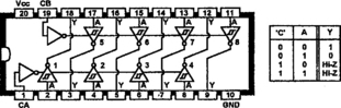
Finally, the 74HC241, 74HC244, and 74LS244 are ‘Octal’ 3-state Schmitt buffers in which the buffers are split into two groups of four, with the mode of each group controlled via a separate input. Figure 6.22 shows the functional diagram and Truth Table of the 74LS244 IC (the 74HC244 is similar, but it has Schmitt-type CA and CB inputs); the IC is really a dual Quad device, in which buffers 1–4 are controlled via the CA terminal, and buffers 5–8 are controlled via the CB terminals.
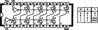
Figure 6.22 Functional diagram and Truth Table of the 74LS244 (or 74HC244) Octal (dual Quad) 3-state Schmitt buffer IC
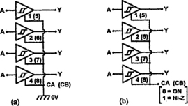
Each of these Quads can be used as a set of simple Schmitt buffers by grounding its control terminal as shown in Figure 6.23(a), or as a ganged set of 3-state Schmitt buffers by using its Control terminal as shown in Figure 6.23(b).
Practical Inverter IC Circuits
The inverter (or NOT gate) is the most basic of all digital logic elements, and is sometimes called an inverting buffer. If you ever need only a few simple inverters, one cheap way to get them is to make them from spare TTL or CMOS NAND or NOR elements, connected as shown in Figure 6.24.
Figure 6.25 lists basic details of some popular inverter ICs. When using these ICs, note that all unused inverters must be disabled by tying their inputs to one of the IC’s supply lines. In CMOS devices, the unused inputs can be tied directly to either supply line, but in TTL devices it is best (for lowest quiescent current consumption) to tie all unused inputs directly to the OV rail; if the unused inverter is a 3-state type, it should (if it has independent control) be set into its ‘normal’ mode via its control input, to minimize current drain.

Dealing now with the individual inverter ICs listed in Figure 6.25, Figure 6.26 shows the functional diagram that is common to the 7404, 74LS04, 74HC04, 74HCU04, and 4069UB Hex inverter ICs. Of these, the 7404 is an ancient Standard TTL IC, the 74LS04 is a modern LS TTL type in which each inverter has a fan-out of 10, the 74HC04 is a fast CMOS type, and the 74HCU04 and 4069UB are unbuffered CMOS types that are suitable for use in linear applications.

Figure 6.27 shows the functional diagram that is common to the 74LS05 and 7406 Hex inverters with o.c. outputs; the 74LS05’s o.c. outputs can handle maximum outputs of only 5.5 volts, but those of the 7406 can handle up to 30 volts.

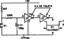
Figure 6.28 shows the functional diagram that is common to three of the most useful of all Hex inverter ICs, the 74LS14 TTL and the 74HC14 and 40106B CMOS Schmitt types. In the 74LS14, the output of each Schmitt inverter is in the logic-1 state until the input rises to an ‘upper threshold’ value of 1.6V, at which point the output switches to logic-0 and locks there until the input is reduced to a ‘lower threshold’ value of 0.8V, at which point the output switches and locks into the logic-1 state again, and so on. Thus, a 74LS14 Schmitt inverter can be made to function as a sine-to-square converter by connecting it as shown in Figure 6.29, where RV1 is used to set the circuit to its maximum sensitivity point, at which a quiescent voltage of 1.2V is set on the inverter’s input.


Figures 6.30 to 6.32 show more simple applications of the 74LS14 IC. Figure 6.30 is a practical version of the Figure 3.6 switch debouncer; it can be activated by a push-button (S1) or toggle (S2) switch, and has an output that goes to logic-1 when the switch is closed. Figure 6.31 is a modified version of the above circuit, with an added inverter stage, and gives a logic-0 output when S1 is closed. Figure 6.32 is yet another modification of the basic circuit, and generates a brief logic-1 ‘switch-on’ output pulse when the circuit’s supply is first connected.


Regarding the 74HC14 and 40106B CMOS Schmitt inverters, these have typical upper and lower threshold values equal to 60% and 40% of the supply voltage respectively. A CMOS Schmitt inverter can thus be made to function as a sine-to-square converter by connecting it as shown in Figure 6.33, where RV1 is used to set the circuit to its maximum sensitivity point, or as a ‘switch-on’ pulse generator (which generates a brief logic-1 ‘switch-on’ output pulse when the circuit’s supply is first connected) by wiring it as shown in Figure 6.34.

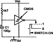
Figure 6.35 shows the functional diagram that is common to the 4049UB and 74HC4049 Hex CMOS inverter ICs. The 4049UB is an unbuffered type, suitable for use in linear applications, and the 74HC4049 is a fast fully buffered general-purpose device.
Figure 6.36 shows the functional diagram and Truth Table of the 4502B. This is a special-purpose 3-state Hex inverter in which the outputs of all six inverters can be set to the logic-0 state by driving the INHIBIT (pin-12) terminal high, or can be set to the high-impedance state by driving the DISABLE (pin-4) terminal high; the IC can be used as a conventional Hex inverter by grounding the INHIBIT and DISABLE pins, or as a normal 3-state inverter by grounding the INHIBIT pin and applying the 3-state control to the DISABLE terminal.

Figure 6.36 Functional diagram and Truth Table of the 4502B Hex 3-state inverter with INHIBIT control
Finally, Figure 6.37 shows the functional diagram and Truth Table of the 74LS240 Octal 3-state Schmitt inverting buffer IC, in which each ‘buffer’ has a fan-out of 30. This IC is actually a dual Quad device, in which inverters 1–4 are controlled via the CA terminal, and inverters 5–8 are controlled via the CB terminal. Each of these Quads can be used as a set of normal Schmitt inverters by grounding its control terminal, or as a ganged set of 3-state Schmitt inverters by using its control terminal as shown in the Truth Table.
Practical AND-gate IC Circuits
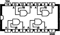
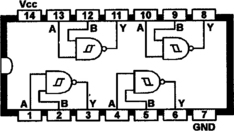
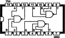
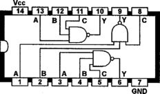
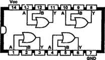
The output of an AND gate goes high (to logic-1) when all of its inputs (A and B and C, etc.) are high. Figure 6.38 lists basic details of several popular AND-gate ICs; of these, the 74LS08, 74HC08, and 4081B (see Figures 6.39 and 6.40) are Quad 2-input types, the 74LS11 and 4073B (see Figures 6.41 and 6.42) are Triple 3-input types, and the 74LS21 and 4082B (see Figures 6.43 and 6.44) are Dual 4-input types.


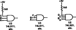
When using AND-gate ICs, each unwanted gate must be disabled by shorting all of its inputs together and tying them to one of the IC’s supply lines. In CMOS ICs, the shorted inputs can be wired directly to either supply line, but in TTL ICs the inputs must (to give minimum quiescent current consumption with good stability) be tied to the positive supply rail via a single 1k0 resistor, as shown in Figure 6.45; a single resistor can be used as a tie-point for large numbers of unwanted inputs.

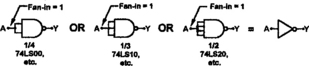
Sometimes, when using 3-input or 4-input AND gate ICs, you may not want to use all of a gate’s input terminals. In this case, the unwanted inputs can be disabled by either tying them high (directly in CMOS gates, or via a 1k0 resistor in TTL types) or by simply shorting them directly to a used input; Figure 6.46 shows examples of 3-input and 4-input TTL AND gates wired for use as 2-input types. Note that the fan-in of a TTL AND gate is an almost constant ‘1’, irrespective of the number of inputs used. Thus, CMOS or TTL AND gates can be converted into non-inverting buffers by simply shorting all of their inputs together; Figure 6.47 shows examples of TTL AND gates used as simple buffers.

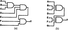
A useful feature of AND gate ICs is that their gates can be directly cascaded, with the output of one gate feeding directly into one input of another gate, to make compound AND gates with any desired number of inputs. Figure 6.48, for example, shows how 2-input AND gates can be cascaded to make 3-input, 4-input, or 5-input AND gates, and Figure 6.49 shows three 3-input or two 4-input gates cascaded to make a single 7-input AND gate.

Practical NAND-gate IC Circuits
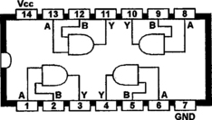
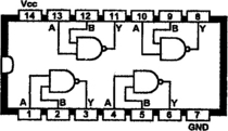
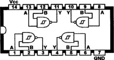
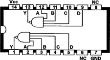
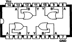
The output of a NAND gate goes low when all of its inputs (A and B, etc.) are high. Figure 6.50 lists basic details of 13 popular NAND-gate ICs; of these, the 74LS00, 74HC00, and 4011B (see Figures 6.51 and 6.52) are standard Quad 2-input types, and the 4093B, 74LS132 and 74HC132 (see Figures 6.53 and 6.54) are Schmitt Quad 2-input types. The 74LS10 and 4023B (see Figures 6.55 and 6.56) are Triple 3-input standard types, the 74LS20 and 4012B (see Figures 6.57 and 6.58) are Dual 4-input standard types, the 74LS30 and 4068B (see Figures 6.59 and 6.60) are 8-input standard types, and the 74HC133 is a 13-input standard type.


When using NAND-gate ICs, each unwanted gate should be disabled by shorting all of its inputs together and tying them to one of the IC’s supply lines. In CMOS ICs, the shorted inputs can be wired directly to either supply line, but in TTL ICs the inputs must (to give minimum quiescent current consumption with good stability) be tied directly to the 0V rail, as shown in Figure 6.61.
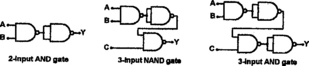
Sometimes, when using NAND gate ICs, you may not want to use all of a gate’s input terminals. In this case, the unwanted inputs can be disabled by either tying them high (directly in CMOS gates, or via a 1k0 resistor in TTL types) or by simply shorting them directly to a used input; Figure 6.62 shows examples of a 3-input TTL NAND gate wired for use as a 2-input type. Note that the fan-in of a TTL NAND gate is an almost constant ‘1’, irrespective of the number of inputs used. Thus, CMOS or TTL NAND gates can be converted into simple inverters by simply shorting all of their inputs together; Figure 6.63 shows examples of TTL NAND gates used as inverters. Also note that NAND gates are fairly versatile elements, as demonstrated in Figure 6.64, which shows ways of using 2-input elements to make a 2-input or 3-input AND gate or a 3-input NAND gate.

Practical OR-Gate IC Circuits
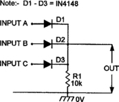
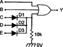
The output of an OR gate goes high when any of its inputs (A or B, etc.) go high. The simplest way to make an OR gate is via a number of diodes and a single resistor, as shown (for example) in the 3-input OR gate of Figure 6.65. The diode OR gate is reasonably fast, very cost-effective, and can readily be expanded to accept any number of inputs by simply adding one more diode to the circuit for each new input.
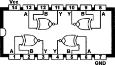
Relatively few dedicated OR-gate ICs are available; Figure 6.66 lists basic details of the six most popular OR-gate ICs; the 74LS32, 74HC32, and 4071B (see Figures 6.67 and 6.68) are Quad 2-input types, the 4075B and 74HC4075 (see Figure 6.69) are Triple 3-input types, and the 4072B (see Figure 6.70) is a Dual 4-input type.


When using OR-gate ICs, each unwanted gate should be disabled by shorting all of its inputs together and tying them to one of the IC’s supply lines. In CMOS ICs, the shorted inputs can be wired directly to either supply line, but in TTL ICs the inputs must (to give minimum quiescent current consumption with good stability) be tied high via a 1k0 resistor, as shown in Figure 6.71.

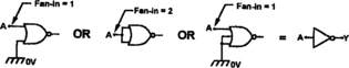
Note that the fan-in of a TTL NOR gate is directly proportional to the number of inputs used, at a fan-in rate of 1-per-input, and that a TTL 2-input OR gate can be made to act as a simple non-inverting buffer by either tying one input to ground or by tying both inputs together, as shown in Figure 6.72, but that the buffer has a fan-in of 1 in the former case, and a fan-in of 2 in the latter. Also note that OR gates can be directly cascaded to make a compound OR gate with any desired number of inputs; Figure 6.73, for example, shows ways of cascading 2-input elements to make OR gates with 3, 4, or 5 inputs, and Figure 6.74 shows a 3-input OR element and a 3-input diode OR gate cascaded to make a compound 5-input OR gate.


Practical NOR-gate IC Circuits
The output of a NOR gate goes low when any of its inputs (A or B, etc.) go high. One easy way to make a NOR gate is to combine a basic diode OR gate with a transistor or IC inverter stage, as shown in the 3-input NOR gate circuit of Figure 6.75. NOR gates of this type are reasonably fast and cost-effective and can easily be expanded to accept any desired number of inputs by simply adding one new diode for each new input.

Figure 6.75 A simple NOR gate can be made by feeding the output of a diode OR gate through a transistor or IC inverter stage
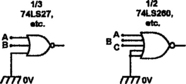
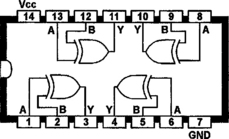
Figure 6.76 lists basic details of the ten most popular NOR-gate ICs; of these, the 74LS02, 74HC02, 4001B and the unbuffered 4001UB (see Figures 6.77 and 6.78) are all Quad 2-input types. The 4025B and the 74LS27 and 74HC27 (see Figures 6.79 and 6.80) are Triple 3-input types, and the 4002B and 74LS260 (see Figures 6.81 and 6.82) are Dual 4-input and 5-input types respectively. The 4078B (Figure 6.83) is an 8-input NOR gate IC.


When using NOR-gate ICs, each unwanted gate should be disabled by shorting all of its inputs together and tying them to one of the IC’s supply lines. In CMOS ICs, the shorted inputs can be wired directly to either supply line, but in TTL ICs the inputs must (to give minimum quiescent current consumption with good stability) be tied directly to the OV rail, as shown in Figure 6.84.
Sometimes, when using NOR gate ICs, you may not want to use all of a gate’s input terminals. In this case, the unwanted inputs are best disabled by shorting them directly to the OV rail, as shown in the examples of Figure 6.85. A NOR gate can be made to act as a simple inverter by either shorting all of its inputs together or by grounding all but one of its inputs; note, however, that the fan-in of a TTL NOR gate is directly proportional to the number of inputs used, so the first method is thus (theoretically) the best, since it offers the lowest fan-in value, as shown in Figure 6.86.
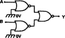
NOR gates are fairly versatile devices. The effective number of inputs of a NOR gate can be increased by applying the extra inputs via a diode or IC OR gate, as shown in Figure 6.87. Figure 6.88 shows various ways of using 2-input elements to make 2-input or 3-input OR gates or a 3-input NOR gate. Note that a NOR gate can be converted into an AND gate by simply inverting all of its inputs, and Figure 6.89 shows how three 2-input NOR gates can be used to make a single AND gate.


Practical EX-OR and EX-NOR IC Circuits
The output of an EX-OR gate goes high only when its two inputs are at different logic levels. The most widely used EX-OR gate ICs are the 74LS86 TTL and the 74HC86 and 4070B CMOS Quad types (see Figures 6.90 and 6.91). If one or more of a CMOS EX-OR IC’s gates are unwanted, it can be disabled by simply grounding both inputs. In the case of a TTL EX-OR IC, unwanted gates are best disabled by grounding one input terminal and tying the other high via a 1k0 resistor, as shown in Figure 6.92, as this results in minimum quiescent current consumption; alternatively, if current drain is not important, both inputs can simply be tied to ground as shown.


EX-OR gates are quite versatile. An EX-OR gate can be made to act as a non-inverting buffer by simply grounding its unused input, as shown in Figure 6.93(a), or as an inverting buffer by tying the unused input high (via a 1k0 resistor in TTL types), as shown in Figure 6.93(b). Thus, two EX-OR gates can be used to make a single EX-NOR gate by connecting them as shown in Figure 6.94, where the right-hand gate is used to invert the output of the left-hand gate; note that Quad EX-NOR CMOS ICs are also available in dedicated IC forms as the 4077B and the 74HC266 (see Figures 6.95 and 6.96), but that the latter IC’s gates have open-drain outputs.

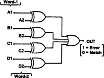
Figures 6.97 and 6.98 show two other useful EX-OR gate applications. In Figure 6.97, four EX-OR gates are fed with a common control signal that enables a 4-bit ‘ABCD’ input code to be presented in the form of either a true (direct) or complement (inverted) ABCD output, thus making the 4-bit True/Complement outputs available via five (rather than eight) terminals. The circuit in Figure 6.98 simply compares the logic states of two 4-bit words and gives a logic-0 output if the two words are identical, and a logic-1 output if they differ.

One of the most important applications of the EX-OR gate is as a binary adder. Figure 6.99 lists the basic rules of binary addition, and Figure 6.100 shows how an EX-OR and an AND gate can be used to make a practical ‘half-adder’ circuit that can add two binary inputs together and generate SUM and CARRY outputs. The circuit is called a ‘half-adder’ because it can perform only a very primitive form of addition that does not enable it to accept a ‘carry’ input from a previous addition stage. A ‘full-adder’ is a far more useful circuit that can accept a ‘carry’ input, perform 2-bit binary addition, and generate a ‘carry’ output; such circuits are fully cascadable, enabling groups of circuits to perform binary addition on digital numbers of a desired ‘bit’ size. Figure 6.101 shows one way of building a 2-bit full-adder circuit, using three EX-OR gates, two AND gates, and an OR gate. In practice, 4-bit full-adders are readily available in the forms of the 74LS283 and 4008B ICs.


Mixed Gate ICs
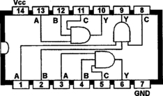
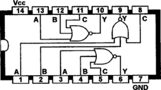
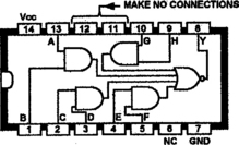
The ‘74’ and ‘4000B’ ranges of ICs include a number of ‘mixed gate’ types that contain gates of more than one type, wired together for use in special applications. The best known of these are ‘AND-OR-INVERT’ (‘AOI’) gates, and examples of these are shown in Figures 6.102 and 6.103. It is unlikely that you will ever need to use an AOI gate, but you may find it useful to learn some of the jargon that is associated with them. Looking first at the 7454 IC of Figure 6.102, note that it has input connections to four 2-input AND gates, and this accounts for the ‘4-wide 2-input AND-’ part of the IC’s title; also note that the outputs of these four AND gates are wired to the inputs of a NOR gate and thence made externally available via pin-8; now, a NOR gate is simply an OR gate with an inverted output, and this fact accounts for the ‘OR-INVERT’ part of the ICs title. Thus, an ‘AND-OR-INVERT’ gate is simply an ‘AND-NOR gate’ with a rather flowery title. The action of the 7454 IC is such that its output is normally high, and goes low only when both inputs to one or more AND gates are high.
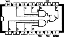
Turning next to the 74LS55 IC of Figure 6.103, note that this has input connections to two 4-input AND gates, and this accounts for the IC’s ‘2-wide 4-input AND-OR-INVERT’ title; the IC’s action is such that its output is normally high, and goes low only when all inputs to at least one AND gate are high.
Returning briefly to the 7454 IC, note that this is a Standard-TTL device, and its data sheet carries a very sinister warning that NO EXTERNAL CONNECTION must be made to pins 11 and 12. Also note that the ‘LS’ version of this device (the 74LS54) has two of its four AND gates configured as 2-input types and two configured as 3-input types, and is sometimes known as a ‘4-wide, 2–3–3–2-input AND-OR-INVERT gate’, and has pin connections, etc., that differ from those shown in Figure 6.102.
A ‘Programmable’ Logic IC
Most logic ICs are dedicated devices that contain a number of ‘fixed’ gates. One very useful exception is the CMOS IC known as the 4048B ‘programmable’ 8-input multifunction gate (see Figure 6.104). This modestly priced (but hard to find) 16-pin IC has two groups of four input terminals, plus an ‘expansion’ input terminal, and is provided with four control (K) pins which let the user select the mode of logic operation, plus a ‘J’ output terminal that enables 4048B ICs to be cascaded, so that two of them make a 16-input gate, or four make a 32-input gate, and so on.

Figure 6.104 Functional diagram (a) and outline (b) of the 4048B multifunction expandable 8-input gate IC
Control input pin Kd (pin-2) enables the user to select either normal or high-impedance 3-state output operation. The remaining three binary control inputs (Ka, Kb, and Kc) enable any one of eight different logic functions to be selected, as shown in the table of Figure 6.105, which also shows how to connect unwanted inputs in each mode of operation. Thus, to make the 4048B act as a normal 6-input OR gate, connect the two unwanted inputs to ground (logic-0), and connect Ka and Kb to ground and Kc and Kd to the positive supply rail. The EXPAND input (pin-15) is normally tied to ground.

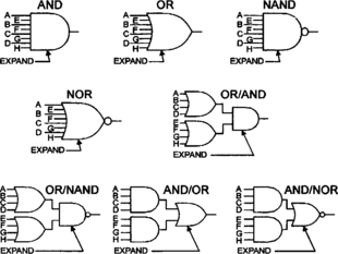
Eight different logic functions are available from the 4048B, as shown in Figure 6.106. Operation in the AND, OR, NAND and NOR modes is quite conventional, but operation in the remaining four modes (OR/AND, OR/NAND, AND/OR, and AND/NOR) is less self-evident. In the latter cases the inputs are split into two groups of four, each of which provides the ‘first’ part of the logic function, but the pair of groups provide the ‘second’ part of the logic function. Thus, in the OR/AND mode, the IC gives a high output only if at least one input is present in the A-to-D group at the same time as at least one input is present in the E-to-H group, etc.
The EXPAND input terminal of the 4048B enables ICs to be cascaded; thus, two ICs can (for example) be made to act as a 16-input gate by feeding the output of one IC into the EXPAND terminal of the other. Note when using ‘expanded’ logic that the input logic feeding the ‘expand’ terminal is not necessarily the same as the overall logic that is required. Thus, an OR ‘expand’ input is needed for expanded NOR or OR operation, a NAND ‘expand’ for AND and NAND operation, a NOR ‘expand’ for OR/AND or OR/NAND operation, and an AND ‘expand’ for AND/OR and AND/NOR operation.
‘Majority Logic’ Circuits
One little known but useful type of logic system is ‘majority’ logic, in which the logic device has an odd (3, 5, 7, etc.) number of inputs and gives an active output only when the majority of these inputs are high, irrespective of which inputs are high. This type of logic is useful in pseudo-intelligent alarms and robotic devices, etc., and may (for example) sound an alarm bell only if at least two of three detectors indicate a ‘fault’ condition, or enable a robot to move only if there is more stimulus to move than there is to stand still, etc.
The best known CMOS majority logic IC is the 4530B Dual 5-input unit (Figure 6.107), each half of which contains a 5-input majority logic element with its output feeding to one input of an EX-NOR gate that has its other input (W) externally available, enabling it to be wired as either an inverting or non-inverting stage. Thus, when ‘W’ is tied to logic-1 the EX-NOR stage gives non-inverting action and the element’s output goes high only when the majority of inputs are high, but when ‘W’ is tied to logic-0 the EX-NOR stage gives an inverting action and the element’s output goes high when the majority of inputs are low. Note that the effective number of inputs of a 4530B element can be reduced by wiring half of the unwanted inputs to logic-1 and the other half to logic-0, as in Figure 6.108(a). Alternatively, the effective number of inputs can be increased by cascading elements, with the output of one element feeding one input of the cascaded element, as in Figure 6.108(b).
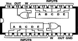
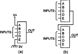
Figure 6.108 The number of effective inputs of a majority-logic circuit can be (a) decreased or (b) increased easily
In practice, the 4530B IC is often hard to find. In this case a majority logic circuit can easily be built by wiring a 3140 CMOS op-amp in the basic configuration of Figure 6.109, which shows a 5-input circuit. Here, the op-amp functions as a voltage comparator in which R6–R7 applies half of the supply voltage to pin-2 of the op-amp, and the five input resistors (which must each be connected to either ground or the positive supply rail) form a potential divider that applies a fraction of the supply voltage to pin-3. This pin-3 voltage is lower than that of pin-2 if the majority of inputs are low, but greater than that of pin-2 if the majority of inputs are high; under this latter condition the op-amp output switches high, and this gives ‘majority logic’ action.
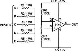
Note that if 5% resistors are used, the Figure 6.109 circuit can be given any odd number of inputs up to a maximum of 11 by simply adding one more 1M0 resistor for each new input. The output of this circuit switches almost fully to zero volts when the output is low, but only rises to within a couple of volts of the positive supply rail when the output is high. In most applications this defect is of little importance; it does mean, however, that elements cannot be cascaded to increase the total number of inputs. This defect can be overcome by using the alternative configuration of Figure 6.110, in which the output is inverted and level shifted by Q1, and the inputs to the op-amp are transposed. The output of this circuit switches to within 50mV of either supply rail, enabling units to be cascaded without limit.

Assertion-level Logic Notion
The reader is already familiar with the fact that an AND or OR gate has an ‘active-high’ output (i.e. the output of an OR gate goes high when any input is high, etc.), and with the MIL/ANSI convention that the addition of a little circle to an OR gate output (etc.) implies that the gate has an ‘active low’ output, as shown in Figure 6.111. Technically, the presence or absence of this ‘little circle’ is known as ‘assertion-level logic notation’, and it can be legitimately applied both to the input or the output of a logic symbol.

Thus, the crude ‘gated pulse generator’ symbol of Figure 6.112(a) implies that the pulse generator is gated on by a HIGH input signal, but the modified symbol of (b) – in which a little circle is added to the generator’s input – implies that this generator is gated on by a LOW input signal, etc.; note that in practice the (a) generator can be made to give the same action as that of (b) by simply inserting an inverter stage between the IN terminal and the input of the generator, as shown in (c), so that a LOW input forces the generator’s input HIGH and gates it on. This system of assertion-level logic notation is in fact very widely used in electronic logic symbology; some examples of its use are shown in Figure 6.113, which deals with mixed logic equivalents.

Mixed Logic Equivalents
When assertion-level logic notation is applied to a simple 2-input AND or OR gate, it can be quickly seen that the gate has four possible input assertion-level sets, i.e. both inputs active-HIGH, or both active-LOW, or one active-HIGH and one active-LOW, or vice versa. Similarly, the gate’s output has two possible assertion-levels (active-HIGH or active-LOW). Thus, a 2-input AND or OR gate has a total of eight possible input/output assertion-levels. If Truth Tables are drawn up for all 16 possible AND and OR gate variations, it becomes apparent that each AND gate variation has a mixed-logic OR gate equivalent, and vice versa, as shown in Figure 6.113. Note in particular that a normal AND gate can be simulated by a NOR gate with both inputs inverted, and that a normal OR gate can be simulated by a NAND gate with both inputs inverted, etc.
Digital ‘Transmission’ Gates
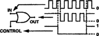
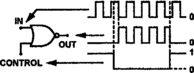
Most logic gate circuits presented in this chapter show the gates used as simple logic state detectors. 2-input AND, NAND, OR and NOR gates can, however, also be used as digital ‘transmission’ gates which pass a digital input signal only when they are ‘opened’ by an appropriate control signal or logic level. Transmission gates are available in four basic types, and the logic symbols of these are shown, together with their logic gate equivalents, in Figure 6.114. The basic transmission gate (a) gives a non-inverted output and can be opened by a logic-1 control signal, and can be simulated by a 2-input AND gate; this transmission gate can be made to give an inverted output, as in (b), by using a NAND gate instead of an AND gate. Another variation of the basic transmission gate is shown in (c); it gives a non-inverted output but is opened by a logic-0 control signal, and can be simulated by a 2-input OR gate; this gate can be made to give an inverted output, as in (d), by using a NOR gate instead of an OR gate. Finally, to conclude this chapter, Figures 6.115 to 6.118 show the precise relationships between the input, output, and control signals of each of these four types of transmission gate.

Figure 6.114 Four basic types of digital transmission gate, with their 2-input logic-gate equivalents
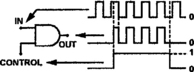
Figure 6.115 AND-type transmission gate is opened by logic-1 control and gives normally-low non-inverted output
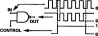
Figure 6.116 NAND-type transmission gate is opened by logic-1 control and gives normally-high inverted output