Analog-to-Digital Signal Conversion
The process of analog-to-digital signal conversion consists of converting a continuous time and amplitude signal into discrete time and amplitude values. Sampling and quantization constitute the steps needed to achieve analog-to-digital signal conversion. To minimize any loss of information that may occur as a result of this conversion, it is important to understand the underlying principles behind sampling and quantization.
2.1 Sampling
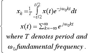
Sampling is the process of generating discrete time samples from an analog signal. First, it is helpful to see the relationship between analog and digital frequencies. Let us consider an analog sinusoidal signal xx (t) = A cos (ωt + ϕ). Sampling this signal at t = nTs, with the sampling time interval of Ts, generates the discrete time signal
where θ = ωTs = ![]()
![]()
![]()
![]() denotes digital frequency with units radians (as compared to analog frequency ω with units radians/sec).
denotes digital frequency with units radians (as compared to analog frequency ω with units radians/sec).
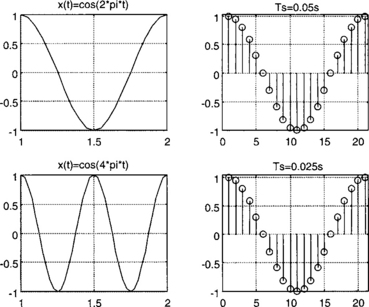
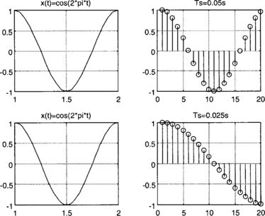
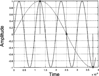
The difference between analog and digital frequencies is more evident by observing that the same discrete time signal is obtained for different continuous time signals if the product ωTs remains the same. (An example is shown in Figure 2-1.) Likewise, different discrete time signals are obtained for the same analog or continuous time signal when the sampling frequency is changed. (An example is shown in Figure 2-2.) In other words, both the frequency of an analog signal and the sampling frequency define the frequency of the corresponding digital signal.
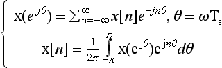
It helps to understand the constraints associated with the above sampling process by examining signals in frequency domain. The Fourier transform pairs in analog and digital domains are given by
Fourier transform pair for analog signals
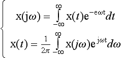
Fourier transform pair for discrete signals
As illustrated in Figure 2-3, when an analog signal with a maximum frequency of fmax(or bandwidth of W) is sampled at a rate of ![]() its corresponding frequency response is repeated every 2π radians, or fs. In other words, Fourier transform in digital domain becomes a periodic version of Fourier transform in analog domain. That is why, for discrete signals, we are only interested in the frequency range 0 – fs/2.
its corresponding frequency response is repeated every 2π radians, or fs. In other words, Fourier transform in digital domain becomes a periodic version of Fourier transform in analog domain. That is why, for discrete signals, we are only interested in the frequency range 0 – fs/2.
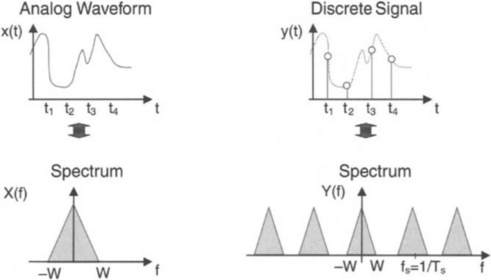
Therefore, in order to avoid any aliasing or distortion of the frequency content of the discrete signal, and hence to be able to recover or reconstruct the frequency content of the original analog signal, we must have fs ≥ 2 fmax. This is known as the Nyquist rate; that is, the sampling frequency should be at least twice the highest frequency in the signal. Normally, before any digital manipulation, a frontend antialiasing analog lowpass filter is used to limit the highest frequency of the analog signal.
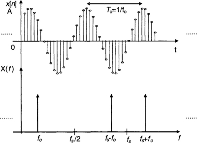
Figure 2-4 shows the Fourier transform of a sampled sinusoid with a frequency of fo. As can be seen, there is only one frequency component at fo. The aliasing problem can be further illustrated by considering an undersampled sinusoid as depicted in Figure 2-5. In this figure, a 1 kHz sinusoid is sampled at fs = 0.8 kHz, which is less than the Nyquist rate. The dashed-line signal is a 200 Hz sinusoid passing through the same sample points. Thus, at this sampling frequency, the output of an A/D converter would be the same if either of the sinusoids were the input signal. On the other hand, oversampling a signal provides a richer description than that of the same signal sampled at the Nyquist rate.
2.1.1. Fast Fourier Transform
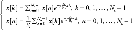
Fourier transform of discrete signals is continuous over the frequency range 0 – fs/2. Thus, from a computational standpoint, this transform is not suitable to use. In practice, discrete Fourier transform (DFT) is used in place of Fourier transform. DFT is the equivalent of Fourier series in analog domain. However, it should be remembered that DFT and Fourier series pairs are defined for periodic signals. These transform pairs are expressed as
Fourier series for periodic analog signals
Discrete Fourier Transform (DFT) for periodic discrete signals
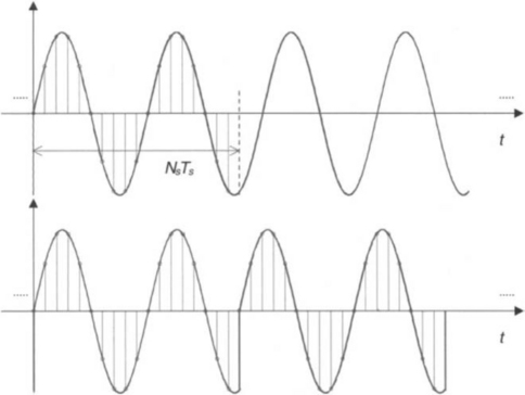
Hence, when computing DFT, it is required to assume periodicity with a period of Ns samples. Figure 2-6 illustrates a sampled sinusoid which is no longer periodic. In order to make sure that the sampled version remains periodic, the analog frequency should satisfy this condition [1]
where m denotes number of cycles over which DFT is computed.
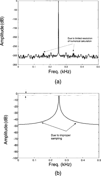
The computational complexity (number of additions and multiplications) of DFT is reduced from Ns2 to NslogNs by using fast Fourier transform (FFT) algorithms. In these algorithms, Ns is considered to be a power of two. Figure 2-7 shows the effect of the periodicity constraint on the FFT computation. In this figure, the FFTs of two sinusoids with frequencies of 250 Hz and 251 Hz are shown. The amplitudes of the sinusoids are unity. Although there is only a 1 Hz difference between the sinusoids, the FFT outcomes are significantly different due to improper sampling.
2.1.2 Amplitude Statistics
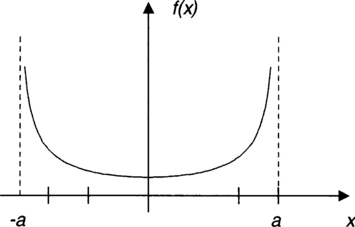
An important property used in signal analysis is amplitude statistics. This statistics reflects the probability density function (pdf) associated with amplitudes of a randomly sampled signal. In other words, this pdf shows the histogram of sample points if the signal is sampled with infinitesimal sampling period. For example, for a sinewave x (t) = a sin(2π fot), its amplitude pdf is given by
This PDF is illustrated in Figure 2-8.
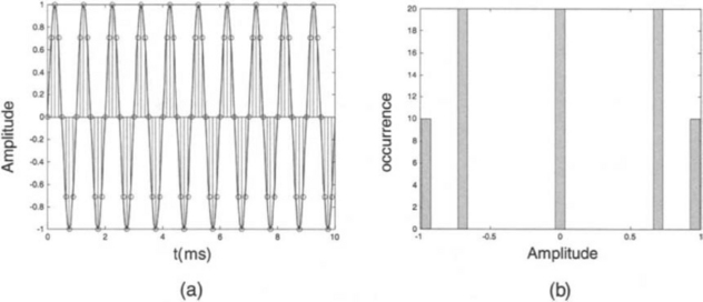
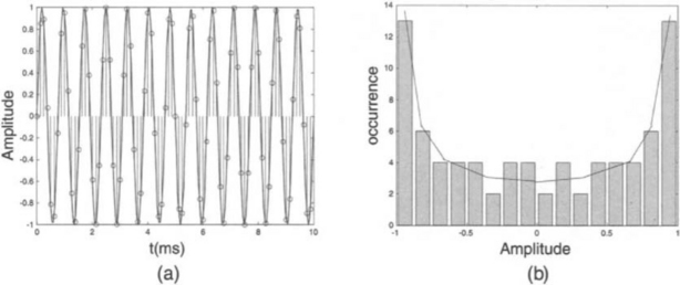
Consider a sinewave with fo = 1 kHz, Ns = 80, and m = 10. As shown in Figure 2-9, the amplitude histogram is not correct due to improper sampling or by repeatedly sampling the same level. In order to avoid this sampling outcome and obtain a proper amplitude statistics, the number of cycles m and the number of samples Ns must be mutually prime. Figure 2-10 shows the amplitude histogram for m = 13.
2.1.3 Harmonics of Distorted Sinewaves
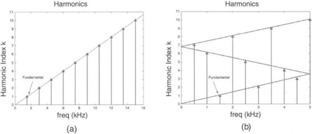
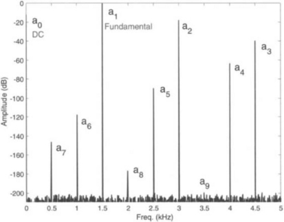
Linear circuits, in general, are not perfectly linear, leading to distortion of output signals. Circuit designers measure this distortion by using a sinewave input. A distorted sinewave, as indicated by Fourier series, contains harmonics. In analog domain, the locations of harmonics on the frequency axis are easy to predict. These locations are at kfo where k denotes harmonic index. However, as a result of sampling, the locations of harmonics are not so easy to predict because of aliasing. The Nyquist rate condition is usually held for the fundamental frequency. Consequently, the sampling frequency may not be sufficient for higher harmonics. Knowledge of the locations of harmonics is of great importance in the interpretation of FFT results, especially for diagnostic purposes. fig. 2-11 shows the effect of sampling on harmonics index. It is seen that the sampling of a distorted sinewave results in consecutive folding of harmonics between 0 and fs/2. Figure 2-12 shows the FFT result of a distorted sinewave with fo = 1.5 kHz and fs = 10 kHz.
2.2 Quantization
An A/D converter has a finite number of bits (or resolution). As a result, continuous amplitude values get represented or approximated by discrete amplitude levels. The process of converting continuous into discrete amplitude levels is called quantization. This approximation leads to an error called quantization noise. The input/output characteristic of a 3-bit A/D converter is shown in Figure 2-13 to see how analog voltage values get approximated by discrete voltage levels.
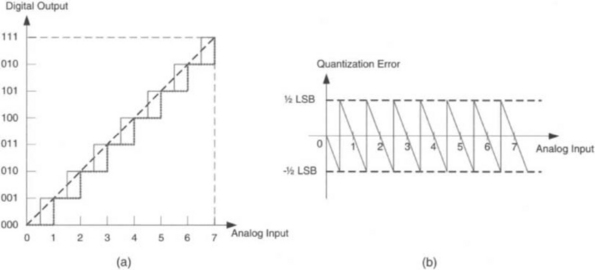
Figure 2-13 Characteristic of a 3-bit A/D converter: (a) input/output static transfer function, and (b) additive quantization noise
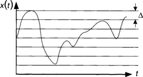
The quantization interval depends on the number of quantization or resolution level, as illustrated in Figure 2-14. Clearly the amount of quantization noise generated by an A/D converter depends on the size of quantization interval. More quantization bits translate into a narrower quantization interval and hence into a lower amount of quantization noise.
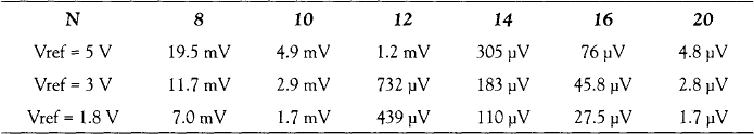
To avoid saturation or out-of-range distortion, the input voltage must be between Vref– and Vref+. The full-scale (FS) voltage or Vref is defined as
and 1 least significant bit (LSB) is given by
where N is the number of bits of the A/D converter. Table 2-1 lists 1 LSB in volts for different numbers of bits and reference voltages. It is interesting to note that a couple of microvolts, which is 1 LSB in a high-resolution A/D converter, can be generated by a dozen electrons in a 1 pF capacitor!
Usually, it is assumed that quantization noise is signal independent and is uniformly distributed over −0.5 LSB and 0.5 LSB. Figure 2-15 shows the quantization noise of an analog signal quantized by a 3-bit A/D converter. It is seen that, although the histogram of the quantization noise is not exactly uniform, it is reasonable to accept the uniformity assumption.
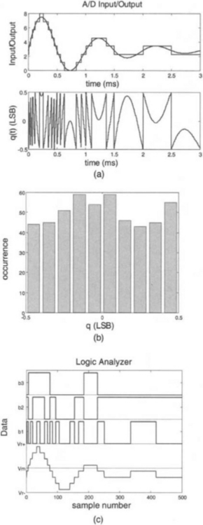
Figure 2.16 shows the FFT of a sinewave before and after the digitization process. The input sinewave is at 250 Hz, with unity amplitude, fs = 1 kHz, and Ns = 512. It is seen that the quantization error raises the noise level.
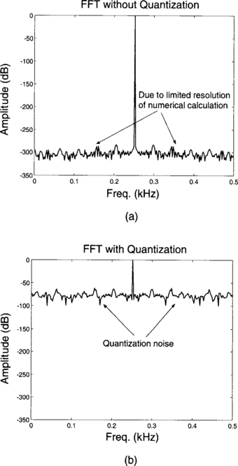
Figure 2-16 Sinewave before and after digitization,fo =250 Hz,fs= 1 kHz,Ns= 512,N= 8-bit: (a) FFT before digitization, and (b) FFT after digitization.
2.2.1 Signal-to-Noise Ratio
Resolution is the term used to describe the minimum resolvable signal level by an A/D converter. The fundamental limit of an A/D converter is governed by quantization noise, which is caused by the A/D converter’s finite resolution. If the output digital word consists of N bits, the minimum step that the converter can resolve is 1 LSB. If we assume quantization error, nq, is a random variable uniformly distributed and independent of the input signal, then we have
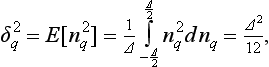
where ![]() indicates quantization noise variance. For a sinusoidal input signal having an amplitude of Am, an ideal A/D converter has a Signal-to-Noise Ratio (SNR) of
indicates quantization noise variance. For a sinusoidal input signal having an amplitude of Am, an ideal A/D converter has a Signal-to-Noise Ratio (SNR) of
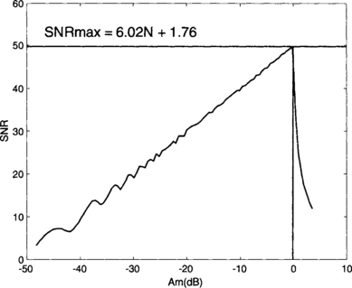
where PS and Pn denote signal and noise power, respectively. It is observed that the quantization SNR is a function of amplitude. The maximum SNR can thus be written as
For instance, an ideal 16-bit A/D converter has a maximum SNR of about 97.8 dB. Quantization noise decreases by 6 dB for each additional bit.
Figure 2-17 shows the SNR of an 8-bit A/D converter as a function of the input amplitude. The maximum occurs when the input sinewave amplitude is equal to one half of the full-scale voltage (scaled to 0 dB).
To better understand the quantization effect, let us assume that the signal is zero mean Gaussian with Vref = Kσx, where σx denotes standard deviation of the signal. By substituting for Vref and σx in (2.11), we obtain
As an example, consider K = 4. The probability of signal samples falling in the 4σx range is 0.954. This means that out of 1,000 samples, 954 samples fall in this range on average. In other words, 46 out of 1,000 samples fall outside the indicated range and hence get represented by the maximum or minimum allowable value.
If the signal is scaled by α, the corresponding signal variance changes to ![]() 1. Hence, the SNR changes to
1. Hence, the SNR changes to
It is important to note that when we perform fractional arithmetic (discussed later in Chapter 6), α is scaled to be less than 1, leading to a lower signal-to-noise ratio. This indicates that quantization noise should be kept in mind when scaling down the input signal. In other words, scaling down to achieve fractional representation cannot be done indefinitely, since, as a result, the signal would get buried in quantization noise.
The interested reader is referred to [2] for more elaborate analysis of quantization noise. For example, for a linear time-invariant system such as a FIR or an IIR filter, it can be shown that the noise variance ![]() at the output of the system, caused by the input quantization noise, is given by
at the output of the system, caused by the input quantization noise, is given by
2.3 Signal Reconstruction
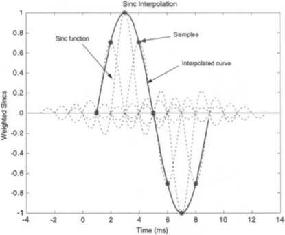
So far, we have examined the forward process of sampling. It is also important to understand the inverse process of signal reconstruction from samples. According to the Nyquist theorem, an analog signal va can be reconstructed from its samples by using the following formula:
One can see that the reconstruction is based on the interpolation of shifted sinc functions. Figure 2-18 illustrates the reconstruction of a sinewave from its samples.
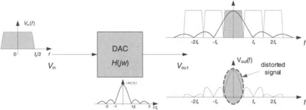
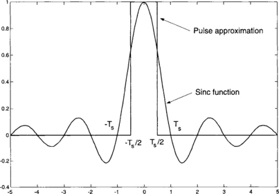
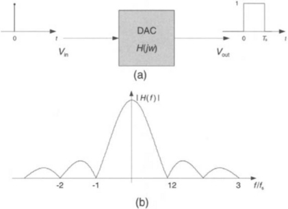
It is very difficult to generate sinc functions by electronic circuitry. That is why, in practice, an approximation of sinc function is used. Figure 2-19 shows an approximation of a sinc function by a pulse, which is easy to realize in electronic circuitry. In fact, the well-known sample and hold circuit performs this approximation. The final stage of a D/A converter is the sample and hold circuit. The transfer function of a D/A converter is
Both the time and frequency domain response of a D/A converter are shown in Figure 2-20.
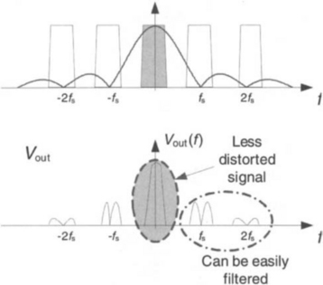
Sample and hold circuits in D/A converters have two inherent non-idealities. First, as illustrated in Figure 2-21, the gain in the desired central band is not constant. It is possible to compensate for this non-ideality by using an inverse filter as part of the DSP component. Another solution is to increase sampling frequency, which results in a narrower relative signal bandwidth. The second non-ideality is caused by the presence of high-frequency replica of the signal spectrum, which can be removed by using a lowpass filter. These solutions are illustrated in Figure 2-22.