TMS320C6X Architecture
The choice of a DSP processor to implement an algorithm in real-time is application dependent. There are many factors that influence this choice. These factors include cost, performance, power consumption, ease-of-use, time-to-market, and integration/interfacing capabilities.
The family of TMS320C6x processors, manufactured by Texas Instruments™, are built to deliver speed. They are designed for million instructions per second (MIPS) intensive applications such as 3G wireless, DSL/cable modems, and digital imaging. Table 3-1 provides a list of currently available fixed-point and floating-point C6x processors at the time of this writing. As can be seen from this table, instruction cycle time, speed, power consumption, memory, peripherals, packaging, and cost specifications vary for different products in this family. For example, the fixed-point C6416-600 version operates at 600 MHz (1.67 ns cycle time), delivering a peak performance of 4800 MIPS. The floating-point C6713-225 version operates at 225 MHz (10 ns cycle time), delivering a peak performance of 1350 MIPS. Figure 3-1 illustrates the processing power of C6x by showing a speed benchmarking comparison with some other common DSP processors.
Table 3-1
Sample C6x DSP product specifications (year 2003).†
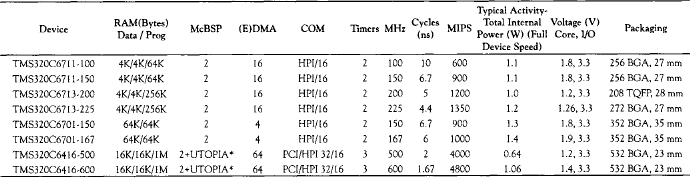
*UTOPIA pins muxed with a third McBSP.
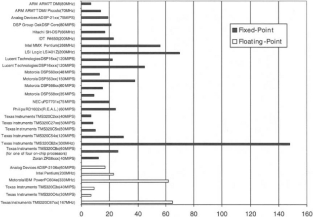
Figure 3-1 BDTImark™ DSP Speed Metric benchmark by Berkeley Design Technology, Inc.1
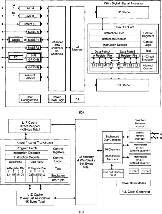
Figure 3-2 shows the block diagrams of the generic C6x, C64x, and C6211/C6711 architectures. The C6x CPU consists of eight functional units divided into two sides: (A) and (B). Each side has a so-called .M unit (used for multiplication operation), a .L unit (used for logical and arithmetic operations), a .S unit (used for branch, bit manipulation and arithmetic operations), and a .D unit (used for loading, storing and arithmetic operations). Some instructions such as ADD can be done by more than one unit. There are sixteen 32-bit registers associated with each side. Interaction with the CPU must be done through these registers. A listing of the C6x instructions, as divided by the four functional units, appears in Appendix A (Quick Reference Guide). These instructions are fully discussed in the TI TMS320C6000 CPU and Instruction Set Reference Guide [1].
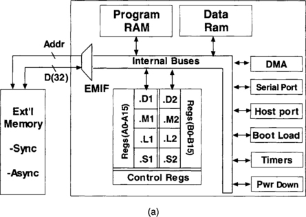
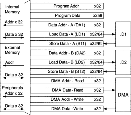
As shown in Figure 3-3, the internal buses consist of a 32-bit program address bus, a 256-bit program data bus accommodating eight 32-bit instructions, two 32-bit data address buses (DA1 and DA2), two 32-bit (64-bit for C64 version) load data buses (LD1 and LD2), and two 32-bit (64-bit for the floating-point version) store data buses (ST1 and ST2). In addition, there are a 32-bit DMA data and a 32-bit DMA address bus. The off-chip, or external, memory is accessed through a 20-bit address bus and a 32-bit data bus.
The peripherals on a typical C6x processor include External Memory Interface (EMIF), DMA, Boot Loader, Multichannel Buffered Serial Port (McBSP), Host Port Interface (HPI), Timer, and Power Down unit. EMIF provides the necessary timing for accessing external memory. DMA allows the movement of data from one place in memory to another place without interfering with the CPU operation. Boot Loader boots the loading of code from off-chip memory or HPI to internal memory. McBSP provides a high-speed multichannel serial communication link. HPI allows a host to access internal memory. Timer provides two 32-bit counters. Power Down unit is used to save power for durations when the CPU is inactive.
3.1 CPU Operation (Dot Product Example)
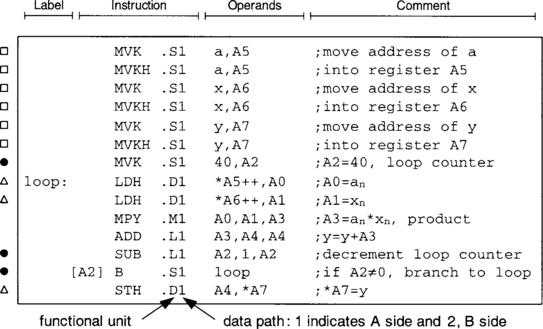
As shown in Figure 3-2, the C6x CPU is divided into two data paths, data path A (or 1), and data path B (or 2). An effective way to understand the CPU operation is by going through an example. Figure 3-4 shows the assembly code for a 40-point dot product y between two vectors a and x, ![]() This code appears in the
This code appears in the
TI Technical Training Notes on TMS320C6x DSP [2]. At this point, it is worth mentioning that the assembler is not case sensitive (i.e., instructions and registers can be written in lower or uppercase).
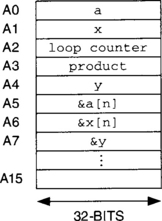
The registers assigned to an, xn, loop counter, product, y, &a [n] (address of an), &x [n] (address of xn), and &y [n] (address of yn) are shown in Figure 3-5. In this example, only the A side functional units and registers are used.
A loop is created by the instructions indicated by •’s. First, a loop counter is set up by using the move constant instruction MVK. This instruction uses the .S1 unit to place the constant 40 in register A2. The beginning of the loop is indicated by the label loop and the end by a subtract instruction SUB to decrement the loop counter followed by a branch instruction B to return to loop.
The subtraction is performed by the .L1 unit and branching by the .S1 unit. The brackets as part of the branch instruction indicate that this is a conditional instruction. All the C6x’s instructions can be made conditional based on a zero or nonzero value in one of the registers: A1, A2, B0, B1, and B2. The syntax [A2] means “execute the instruction if A2 ≠ 0“, and [!A2] means “execute the instruction if A2 = 0”. As a result of these instructions, the loop is repeated 40 times.
Considering that the interaction with the functional units is done through the A-side registers, these registers must be set up in order to start the loop. The instructions labeled by ![]() ’s indicate the necessary instructions for doing so. MVK and MVKH are used to load the address of an, xn, and y into the registers A5, A6, and A7, respectively. These instructions must be done in the order indicated to load the lower 16 bits of the full 32-bit address first, followed by the upper 16 bits. These registers are used as pointers to load an, xn into the A0, A1 registers and store y from the A4 register (instructions labeled by δ). The C programming language notation * is used to indicate a register is being used as a pointer. Depending on the datatype, any of the following loading instructions can be used: bytes (8-bit) LDB, halfwords (16-bit) LDH, or words (32-bit) LDW. Here, the data is assumed to be halfwords. The loading/storing is done by the .D1 unit, since .D units are the only units capable of interacting with data memory.
’s indicate the necessary instructions for doing so. MVK and MVKH are used to load the address of an, xn, and y into the registers A5, A6, and A7, respectively. These instructions must be done in the order indicated to load the lower 16 bits of the full 32-bit address first, followed by the upper 16 bits. These registers are used as pointers to load an, xn into the A0, A1 registers and store y from the A4 register (instructions labeled by δ). The C programming language notation * is used to indicate a register is being used as a pointer. Depending on the datatype, any of the following loading instructions can be used: bytes (8-bit) LDB, halfwords (16-bit) LDH, or words (32-bit) LDW. Here, the data is assumed to be halfwords. The loading/storing is done by the .D1 unit, since .D units are the only units capable of interacting with data memory.
Note that the pointers A5 and A6 need to be post-incremented (C notation), so that they point to the next values for the next iteration of the loop. When registers are used as pointers, there are several ways to perform pointer arithmetic. These include pre- and post-increment/decrement options by some displacement amount, where the pointer is modified before or after it is used (for example, *++A1 [disp] and *A1++ [disp]). In addition, a pre-offset option can be performed with no modification of the pointer (for example, *+A1 [disp]). Displacement within brackets specifies the number of data elements (depending on the datatype), whereas displacement in parentheses specifies the number of bytes. These pointer offset options are listed in Figure 3-6 together with some examples.
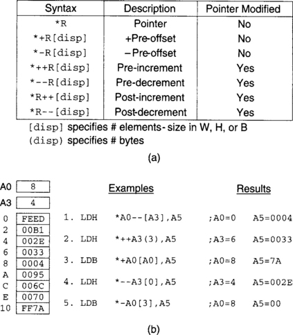
Figure 3-6 (a) Pointer offsets, (b) pointer examples (note: instructions are independent, not sequential).†
Finally, the instructions MPY and ADD within the loop perform the dot product operation. The instruction MPY is done by the .M1 unit and ADD by the .L1 unit. It should be mentioned that the above code as is will not run properly on the C6x because of its pipelined CPU, which is discussed next.
3.2 Pipelined CPU
In general, it takes several steps to perform an instruction. Basically, these steps are fetching, decoding, and execution. If these steps are done serially, not all of the resources on the processor, such as multiple buses or functional units, are fully utilized. In order to increase throughput, DSP CPUs are designed to be pipelined. This means that the foregoing steps are carried out simultaneously. Figure 3-7 illustrates the difference in processing time for three instructions executed on a serial or non-pipelined and a pipelined CPU. As can be seen, a pipelined CPU requires fewer clock cycles to complete the same number of instructions.
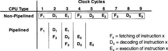
On the C6x processor, fetching consists of four phases, each requiring a clock cycle. These include generate fetch address (denoted by F1), send address to memory (F2), wait for data (F3), and read opcode from memory (F4). Decoding consists of two phases, each requiring a clock cycle. These are dispatching to appropriate functional units (denoted by D1), and decoding (D2). Due to the delays associated with the instructions multiply (MPY – 1 delay), load (LDx – 4 delays), and branch (B – 5 delays), the execution step may consist of up to six phases (denoted by E1 through E6), accommodating a maximum of 5 delays. Hence, as shown in Figure 3-8, the F step consists of four, the D step of two, and the E step of six possible substeps, or phases.

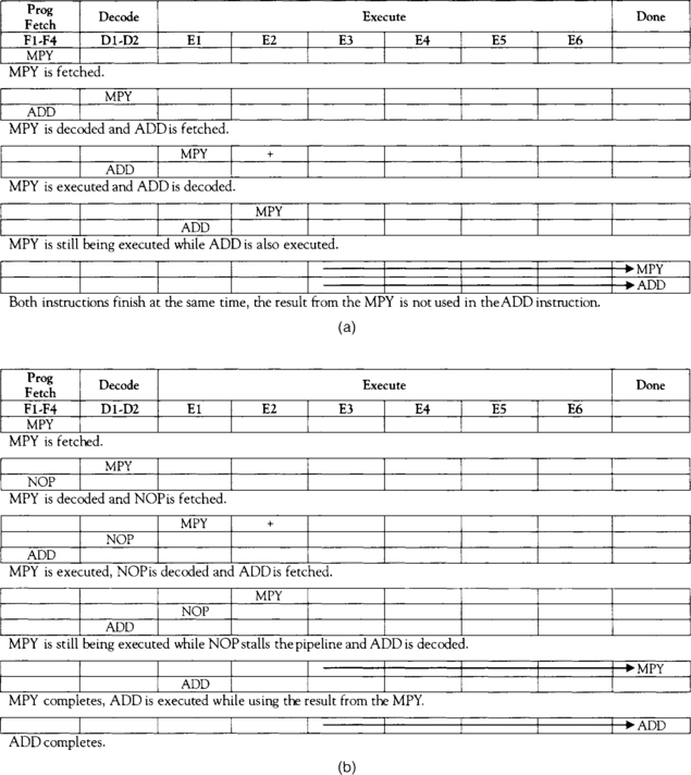
When the outcome of an instruction is used by the next instruction, an appropriate number of NOPs (no operation or delay) must be added after multiply (one NOP), load (four NOPs/or NOP 4), and branch (five NOPs/or NOP 5) instructions in order to allow the pipeline to operate properly. Therefore, for the above example to run on the C6x processor, appropriate NOPs, as shown in Figure 3-9, should be added after the instructions MPY, LDH, and B.
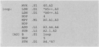
Figure 3-10 illustrates an example of a pipeline situation that requires adding an NOP. The plus signs indicate the number of substeps or latencies required for the instruction to be completed. In this example, it is assumed that the addition operation is done before one of its operands is made available from the previous multiply operation, hence the need for adding a NOP after the MPY. Later on, it will be seen that as part of code optimization, NOPs can be reduced or removed leading to an improvement in efficiency.
3.3 VelociTI
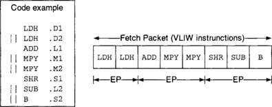
The C6x architecture is based on the very long instruction word (VLIW) architecture. In such an architecture, several instructions are captured and processed simultaneously. This is referred to as a fetch packet (FP). (See Figure 3-11.)
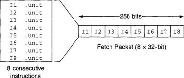
The C6x uses VLIW, allowing eight instructions to be captured simultaneously from on-chip memory onto its 256-bit wide program data bus. The original VLIW architecture has been modified by TI to allow several so-called execute packets (EP) to be included within the same Fetch Packet, as shown in Figure 3-12. An EP constitutes a group of parallel instructions. Parallel instructions are indicated by double pipe symbols (||), and, as the name implies, they are executed together, or in parallel. Instructions within an EP move together through every stage of the pipeline. This VLIW modification is called VelociTI. Compared with VLIW, VelociTI reduces code size and increases performance when instructions reside off-chip.
3.4 C64x DSP
The C64x is a more recently released DSP core, as part of the C6x family, with higher MIPS power operating at higher clock rates. This core can operate in the range of 300-1000 MHz clock rates, giving a processing power of 2400-8000 MIPS. The clock rate is expected to increase to 1.1 GHz and higher, leading to a processing rate of 8800+ MIPS. The TI website http://www.ti.com/provides the C64x speedups obtained over the C62x for various wireless communication and digital imaging algorithms. Such speedups are achieved due to many enhancements, some of which are mentioned here.
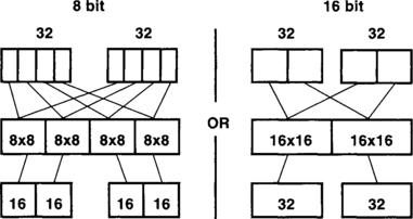
Per CPU data path, the number of registers is increased from 16 to 32, A0–A31 and B0–B31. These registers support packed datatypes, allowing storage and manipulation of four 8-bit or two 16-bit values within a single 32-bit register.
Although the C64x is code compatible with the C62x, (i.e., all the C62x instructions run on the C64x), the C64x can run additional instructions on packed datatypes, boosting parallelism. For example, the new instruction MPYU4 performs four, or quad, 8-bit multiplications, or the instruction MPY2 performs two, or dual, 16-bit multiplications in a single instruction cycle on a .M unit. This packed data processing capability is illustrated in Figure 3-13. Table 3-2 provides a listing of the C64x packed data instructions.
Table 3-2
A listing of C64x packed data instructions.†
| Operations | Quad 8-bit | Quad 16-bit |
| Multiply | x | x |
| Multiply with Saturation | x | |
| Addition/Subtraction | x | x |
| Addition with Saturation | x | x |
| Absolute Value | x | |
| Subtract with Absolute Value | x | |
| Compare | x | x |
| Shift | x | |
| Data pack/Unpack | x | x |
| Data pack with Saturation | x | x |
| Dot Product with optional negate | x | x |
| Min/Max/Average | x | x |
| Bit-expansion (Mask generation) | x | x |
Additional hardware has been added to each functional unit on the C64x for performing ten special purpose instructions to accelerate key functions encountered in wireless and digital imaging applications. For example, the instruction GMPY4 allows four 8-bit Galois-field multiplications in a single instruction as part of the Reed-Solomon decoding. Table 3-3 provides a list of these special purpose instructions.
Table 3-3
C64x special purpose instructions.†
| Instruction | Description | Example Application |
| BITC4 | Bit count | Machine vision |
| GMPY4 | Galois Field MPY | Reed-Solomon support |
| SHFL | Bit interleaving | Convolution encoder |
| DEAL | Bit deinterleaving | Cable modem |
| SWAP4 | Byte swap | Mixed Multiprocessor support |
| XPNDx | Bit expansion | Graphics |
| MPYHIx, MPYLIx | Extended precision 16×32 MPYs | Audio |
| AVGx | Quad 8-bit, Dual 16-bit average | Motion compensation |
| SUBABS4 | Quad 8-bit Absolute of differences | Motion estimation |
| SSHVL, SSHVR | Signed variable shift | GSM |
In addition, the functionality of each functional unit on the C64x has been improved leading to a greater orthogonality, or generality, of operations. For example, the .D unit can perform 32-bit logical operation just as the .S and .L units, or the .M unit can perform shift and rotate operations just as the .S unit. The C64x .S unit is capable of performing additional branching instructions, such as branch positive BPOS. Furthermore, the C64x allows multiple units on one side to read the same crosspath source from the other side.
The C64x supports 64-bit loads and stores with a single instruction. There are four 32-bit paths for loading data to the registers. LD1a and LD2a are the load paths for 32 LSBs (least significant bits) on side A and B, respectively, and LD1b and LD2b for 32 MSBs (most significant bits). Similarly, ST1a, ST1b, ST2a, ST2b are the 32-bit store paths for storing data from memory. The C64x also allows nonaligned loads and stores, meaning that loading and storing of words and double words can be done on any byte boundary by using nonaligned load and store instructions. Figure 3-14 provides a comparison between the data paths of the C62x and C64x CPUs.
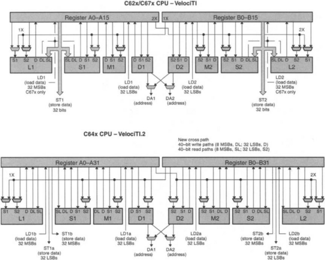
Figure 3-14 Data paths of C62x/67x and C64x (S1=sourcel, S2=source2, D=destination, SL=source long, DL=destination long).†
Finally, similar to the C6211, the C64x contains a 2-level cache, allowing it to make a better use of the CPU speed when interacting with off-chip memory that has a lower speed.
1The BDTImark is a summary measure of DSP speed, distilled from a suite of DSP benchmarks developed and independently verified by Berkeley Design Technology, Inc. A higher BDTImark score indicates a faster processor. For a complete description of the BDTImark and underlying benchmarking methodology, as well as additional BDTImark scores, refer to http://www.bdti.com. © 2000 Berkeley Design Technology, Inc.