Frame Processing
When it comes to processing frames of data (for example, in doing FFT and block convolution), triple buffering is an efficient data frame handling mechanism. While samples of the current frame are being collected by the CPU in an input array via an ISR, samples of the previous frame in an intermediate array can get processed during the time left between samples. At the same time, the DMA can be used to send out samples of a previously processed frame available in an output array. In this manner, the CPU is used to set up the input array and process the intermediate array while the DMA is used to move processed data from the output array. At the end of each frame or the start of a new frame, the roles of these arrays are interchanged. The input array is reassigned as the intermediate array to be processed, the processed intermediate array is reassigned as the output array to be sent out, and the output array is reassigned as the input array to collect incoming samples for the current frame. This process is illustrated in Figure 9-1.

9.1 Direct Memory Access
Many DSP chips are equipped with a Direct Memory Access resource acting as a co-processor to move data from one part of memory into another without interfering with the CPU operation. As a result, the chip throughput is increased since, in this manner, the CPU can process and the DMA can move data without interfering with each other.
Depending upon the DSP platform used, there are two different DMAs called DMA and EDMA (enhanced DMA). The differences between them and their configurations are stated in the following subsections.
9.1.1 DMA
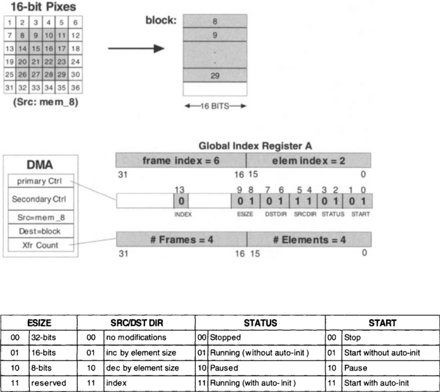
The C6x01 DSP provides four DMA channels. Each DMA channel has its own memory-mapped control registers which can be set up to move data from one place to another place in memory. Figure 9-2 shows the DMA control registers consisting of the Primary Control, Secondary Control, Source Address, Destination Address, and Transfer Counter registers. These registers contain the information regarding source and destination locations in memory, number of transfers, and format of transfers. As shown in Figure 9-2, in addition to the DMA control registers, there are several global registers shared by all DMA channels.

An example is presented here to show how some of the fields of the DMA registers are set for block or frame processing. More details on all the fields are available in the TI TMS320C6x Peripherals Reference Guide [1]. It is possible to transfer a block of data consisting of a number of frames, which in turn consist of a number of elements. Elements here mean the smallest piece of data. The example shown in Figure 9-3 illustrates the DMA register setup for transferring a block of data (this can be viewed as image data) consisting of four frames (rows), while each frame consists of four elements (16-bit pixels). Figure 9-3 also provides the options for some of the fields of the Primary Control Register, Transfer Counter Register, and Global Index Register. Source/destination address fields can be incremented or decremented by an element size or by an index as specified in the global register. The element size field is used to indicate the datatype. The Transfer Counter Register contains the number of frames and elements. In this example, the element size field of the Primary Control Register is set to 01 (halfwords), the source address field to 11 (index option for accessing next value), and the destination to 01 (increment option for writing consecutively). As specified in the Transfer Counter Register, the data transfer in this example consists of four frames, and each frame consists of four elements. The global register A (chosen by the index field) contains the element as well as the frame index. In this example, the element index is set to 2 to increase addresses by 2 bytes or element size, and the frame index to 6 bytes to get to the next frame, since at the end of a frame the pointer points to the beginning of the last element of that frame.
9.1.2 EDMA
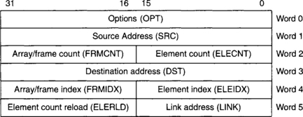
C6711/C6713/C6416 DSKs possess EDMA. The number of EDMA channels are 16 on C671X, and 64 on C64x. As compared with DMA, EDMA provides programmable priority, and the ability to link data transfers. By using the EDMA controller, data can be transferred from/to internal memory (L2 SRAM), or peripherals, to/from external memory spaces efficiently without interfering with the CPU operation. Typically, block data transfers and transfer requests from peripherals are performed via EDMA. Figure 9-4 illustrates the EDMA registers used for its configuration.
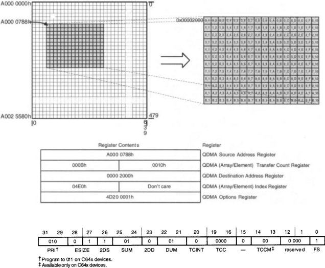
Also, EDMA has a feature called quick DMA (QDMA), which provides a fast and efficient way to transfer data for applications such as data requests in tight loop algorithms. QDMA allows single, independent transfers for quick data movement, rather than periodic or repetitive transfers, as done by EDMA channels. Figure 9-5 illustrates an example of 2-D to 1-D data transfer. A 166 × 12 subframe of a 640 × 480 video data (16-bit pixels), stored in the external memory, is transferred to the internal L2 RAM by using QDMA. Similar to the DMA example, the array index denotes the space between the subframe arrays. Thus, the array index is 2 * (640 – 16) = 1248 (4E0h). In the QDMA Options register, the priority level is set to be low, element size to 16-bit half-word. The source is specified as two-dimensional with address increment, and the destination is specified as one-dimensional with address increment. The transfer complete interrupt (TCINT) field is disabled and the channel is synchronized by setting the frame synchronization field (FS) to 1. For a more detailed description of EDMA and QDMA, refer to Applications Using the TMS320C6000 Enhanced DMA [2].
9.2 DSP-Host Communication
9.2.1 Host-Port Interface (HPI) on C6711 DSK
The HPI on C6711 DSK is a 16-bit-wide parallel port through which a PC host can directly access the DSP memory and peripherals. No specific configuration is required for the HPI communication on the DSP side since the host program acts as master.
A program on the PC host is written here in Microsoft® Visual C++® using the library dsk6×l11hpi.lib, which is a part of CCS. In this program, a sample configuration file, ti_ppdsk.cfg, is accessed to open the device handle. After opening the DSK and the HPI with the dsk6x_open ( ) and dsk6x_hpi_open ( ) APIs, respectively, the memory of the DSP is read by the dsk6x_hpi_read ( ) API based on the length and starting address parameters. This program appears below.
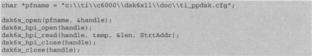
In order to build this program, the library dsk6×l11hpi.lib should be included in the project and the Win32 DLL dsk6×l11hpi.dll should be placed in the same folder where the program is located.
Bearing in mind that CCS already uses the HPI to load and run the program, the access should be returned before the host program runs on the PC. Thus, CCS should be closed before the host program is executed. The DSP target program is then loaded and run by the host program instead of CCS.
9.2.2 HPI on C6701 EVM
On the C6701 EVM, there are two 32-bit FIFO (first in, first out) registers, called FIFO-read and FIFO-write, in the PCI controller of the EVM board through which the PC host and the C6x can communicate. The FIFO-read is used for data transfer from the host to the DSP and the FIFO-write for data transfer from the DSP to the host. The initialization of the FIFO is done through the memory mapped FIFO status register. The communication can be simply achieved by using the supplied Write-FIFO_DMA ( ) function as part of Lab6.
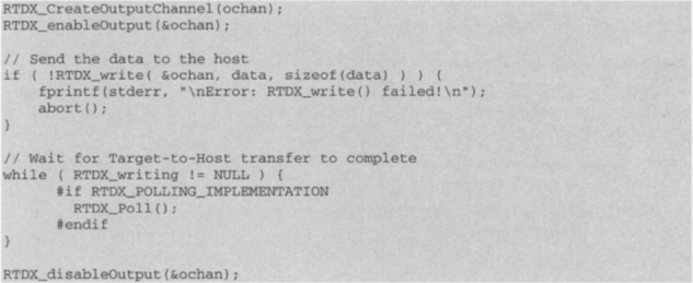
9.2.3 Real-Time Data Exchange (RTDX)
Since the HPI on the C6713/C6416 DSKs requires an external interface through the PCI/HPI port, RTDX is used here as an alternative way to communicate between the host and the DSP. On these platforms, CCS communicates with the DSK through an embedded JTAG emulator with a USB host interface.
RTDX details are discussed in Chapter 10. To use RTDX, first a channel needs to be created by calling the function RTDX_CreateOutputChannel ( ). Then, data can get transferred to the host in real-time by calling the RTDX_write ( ) API, as shown below.
Lab. 6 Fast Fourier Transform
Operations such as DFT or FFT require that a frame of data be present at the time of processing. Unlike filtering, where operations are done on every incoming sample, in frame processing N samples are captured first and then operations are performed on all N samples.
To perform frame processing, a proper method of gathering data and of processing and sending data out is required. The processing of a frame of data is not usually completed within the sampling time interval, rather it is spread over the duration of a frame before the next frame of data is gathered. Hence, incoming samples must be stored into a separate buffer other than the one being processed. Also, another buffer is needed to send out a previously processed frame of data. As explained earlier, this can be achieved by triple buffering involving three buffers: input, intermediate, and output.
To do triple buffering on the C6x, the sampling shell program in Lab 2 is modified to incorporate an endless loop revolving around the rotation of three buffers. The buffers rotate every time the input buffer is full so that a new frame of N sampled data is passed to the intermediate buffer for processing and a previously processed frame is passed to the output buffer for transmission. The following modifications of the shell program achieve this:
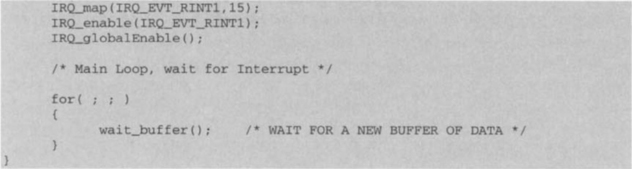
The preceding code shows how an endless loop is added to the shell program. Here, most of the initializations for the codec and McBSP have not been shown to make the code easier to follow. Once the serial port is initialized, the three arrays are allocated in memory and initialized to zero. The program then goes into an endless loop where the function wait_buffer ( ), shown next, is executed endlessly:
This function checks on the global variable index to do the rotation of the arrays and to start processing. When the input array becomes full (indicated by index), the arrays are rotated and the intermediate array gets set for processing. The comment //Function call here … indicates where the processing function such as FFT should be placed.
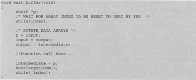
The ISR is also modified as shown in the next code block. In the ISR, EDMA is used to transfer a sample from DRR to DXR without using the MCBSP_write ( ) API. Note that index is incremented within the ISR.

To configure EDMA for reading from DRR and writing back to DXR, the source and destination address should refer to DRR1 and DXR1, respectively. In the Options Parameter register, the priority level is set to high, element size to 32-bit, with one-dimensional source and destination. No incrementing of address for source or destination is necessary since the source and destination are fixed-address memory mapped registers. Similar to the other CSL peripherals, EDMA is opened and configured with the EDMA_open ( ) and EDMA_config ( ) APIs. The EDMA_setChannel ( ) API triggers the EDMA channel. After transmitting data, the opened channel should be closed with EDMA_close ( ).
For FFT processing purposes, the data read from DRR are left-shifted by 16 bits to get rid of the data portion corresponding to the right channel. To store in Q-15 format, it is shifted back right by 16 bits. The input samples are then placed into the input array to build a frame of length BUFFLENGTH. The variable index is incremented every time a new input sample is read. This variable is reset to zero when the input buffer becomes full, that is, index reaches BUFFLENGTH. This reset causes the program to go out of the while (index) loop in the function wait_buffer ( ). Then, the rest of the program in wait_buffer ( ) gets executed.
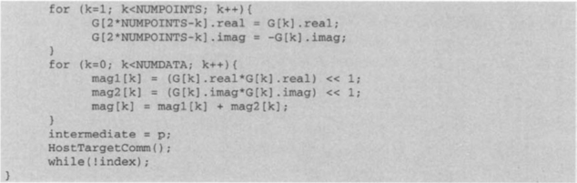
Now, let us go back to wait_buffer ( ). After index is reset to zero, the input buffer is reassigned to a pointer named p. This reassignment is necessary for the //Function call here … part to avoid any conflict with the ISR. Note that the ISR uses the input buffer to receive new samples. If say the FFT function processes the data in the input buffer, wrong results may be produced, because the ISR may change the content of the input buffer anytime. This malfunction may occur because the ISR runs on a higher priority basis, while the FFT function runs on a lower priority basis. Following the p= input statement, the output buffer is reassigned to the input buffer. This reassignment allows the ISR to use the output buffer to receive and store new incoming samples. Notice that the data in the output buffer is sent out by the DMA. The next reassignment output = intermediate is necessary in order to send the processed data in the intermediate buffer to the DXR.
After the data is processed in //Function call here …, the pointer p is reassigned to the intermediate buffer for it to point to the processed samples. The data in the intermediate buffer is sent out by the function HostTargetComm ( ) as part of the wait_buffer ( ) function. The while loop while (! index) at the end of wait_buffer ( ) ensures that a frame is processed only once. In the absence of a new sample in the DRR, index remains zero and the program waits at while (! index) because ! index is TRUE. When a new sample arrives in the DRR, index is incremented and the program gets out of wait_buffer ( ) and falls into the loop in main ( ). There it waits for a new frame.
For communication with a PC host, two different methods are mentioned here depending on the target platform (DSK or EVM) used. When using EVM, the communication is done through the memory mapped I/O address, PCI FIFO, corresponding to the PC PCI channel. There are two 32-bit FIFO (first in first out) registers, called FIFO-read and FIFO-write, in the PCI controller of the EVM board through which the PC host and the C6x may communicate. The FIFO-read is used for data transfer from the PC host to the DSP and the FIFO-write for data transfer from the DSP to the PC host. The initialization of the FIFO is done through the memory mapped FIFO status register. The communication is achieved by using the HostTargetComm ( ) function. This function utilizes the C6x’s DMA capability to send the intermediate array to the host through the FIFO registers. The following provides the code for doing so:
![]()
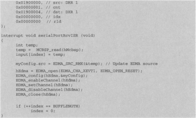
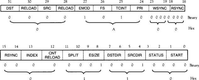
The two DMA API functions dma_reset ( ) and dma_init ( ) are used to initialize the DMA for data transfer between the intermediate array and the FIFO. A single frame of samples of length 128 is transferred as indicated by the content of the Transfer Counter Register (TCR). The dma_reset ( ) API resets all the DMA registers to their power-on reset states. The dma_init ( ) API initializes a selected DMA channel by assigning appropriate values to its control registers. Here, the first argument of the dma_init ( ) API is used to select the DMA channel 2. The second argument sets the Primary Control Register to 0×l0A000110u, as shown in Figure 9-6. This value is specified based upon the following: EMOD bit is set to 1 to pause the DMA channel during an emulation halt. TCINT bit is set to 1 to enable the transfer controller interrupt. The element size is 16 bits, so ESIZE bits are set to 01. SRC DIR bits are set to 01 to increment the source address by element size in bytes. The third argument of the dma_init ( ) API sets the Secondary Control Register. SX IE and FRAME IE bits of this register are set to 1 to enable the DMA channel interrupt. The fourth argument of the dma_init ( ) API assigns the intermediate array as the source address. The fifth argument is set to 0×l01710000u, which is the address of the EVM PCI interface, through which the host program reads the output. The last argument sets the Transfer Counter Register to 0×l00010080u. The upper 16 bits specify the number of frames. Here, these bits are set to 0×l0001u in order to send out one frame at a time. The lower 16 bits are set to 0×l0080u for having 128 elements in a frame. Finally, the function HostTargetComm ( ) calls the macro DMA_START ( ) to activate the DMA channel 2. This macro sets the START field of the Primary Control Register to 01.
When using C6711 DSK, the communication is done through the parallel port. In order to implement a function equivalent to HostTargetComm, the host-port interface (HPI) is utilized instead of DMA. HPI is a 16-bit wide parallel port through which a PC host can directly access the C6x memory and peripherals. No specific configuration is required for the HPI communication on the DSP side, since the host program acts as master. However, the intermediate pointer should be passed to the host for having a proper memory access, because the triple buffering scheme keeps changing the address of the physical memory where the array of intermediate values is stored. Also, a variable should be used as a flag for data synchronization. A fixed physical memory address, say 0×l00000200, is allocated as a separate section, .hpi, to allow access from the host. This way the processed data can always be read by referring to its address stored in this section. Thus, the linker command file and the function HostTargetComm need to be changed as follows:
By using a function generator and an oscilloscope, the operation of the modified sampling program can be verified. When using EVM, to get data from the FIFO on the host side and display them on the PC monitor, a program called Host.exe running on the PC host is provided on the accompanying CD-ROM. This program utilizes the evm6x_read ( ) API from the EVM host support library. When using DSK, the API function dsk6x_hpi_read ( ) is used instead. This program, which is written in Microsoft™ Visual C++ using a Dialog wizard, starts a thread that continuously reads data from the pointer in the .hpi section and plots it on the monitor. The APIs used in the program are part of CCS.
The communication between the PC host and the DSP is achieved via RTDX for C6416/C6713. The accompanying CD-ROM contains the corresponding source codes with the RTDX APIs. A detailed description of RTDX appears in Chapter 10. The host application program for displaying and analyzing data via RTDX is also on the accompanying CD-ROM. Descriptions and examples of developing host application programs with Visual Basic, Visual C++, MATLAB, or Microsoft® Excel can be found at the TI website.
L6.1 DFT Implementation
DFT can be simply calculated from the equation
where WN = e−j2π/N. This equation requires N complex multiplications and N – 1 complex additions for each term. For all N terms, N2 complex multiplications and N2 – N complex additions are needed. As is well known, this method is not efficient since the symmetry properties of the transform are not utilized. However, it is useful to implement the equation on the C6x as a comparison to the FFT implementation. The graphing capability of CCS is used here for this purpose. This is carried out in an offline manner because the amount of time required to do the DFT exceeds the duration of a frame capture.
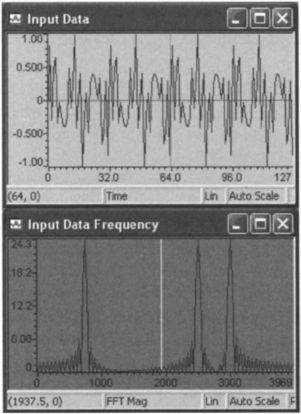
First, a simple composite signal is generated in MATLAB with the frequency components at 750 Hz, 2500 Hz, and 3000 Hz. Saving two periods of this signal sampled at 8000 Hz results in a 64-point signal. Figure 9-7 shows the signal read into CCS and plotted using its graphing capability. The frequency content of the signal is also plotted based on a built-in FFT option.
The DFT code used is the one appearing in the TI Application Report SPRA291 [1]. Here is the code:
![]()
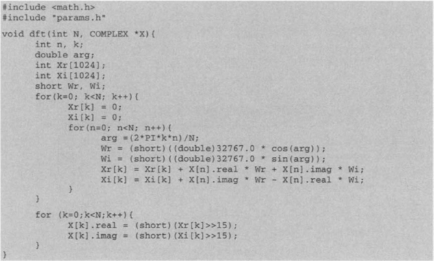
In order to use this code, the input has to be represented as complex numbers. This is done using a structure definition to create a complex variable with components real and imag. The main program used to perform DFT is as follows:
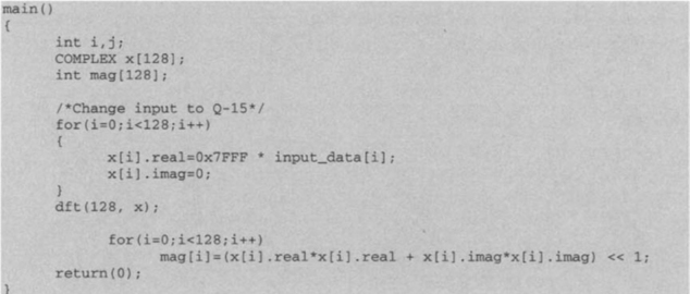
In this program, the input is converted to Q-15 format and stored in the complex structure, which is then used to call the DFT function. The magnitude of the DFT outcome is shown in Figure 9-8. As expected, there are three spikes, at 750Hz,

2500Hz, and 3000Hz. Notice that this code is quite inefficient, as it calculates each twiddle factor using the math library at every iteration. Running this code from the external SDRAM results in an execution time of about 1.6 × 10⁹ cycles for a 128-point frame. As a result, the preceding DFT code cannot be run in real-time on the DSK, since only 18,750 × 128 = 2.4 × 10⁶ cycles are available to perform a 128-point transform.
L6.2 FFT Implementation
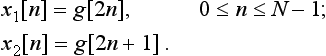
To allow real-time processing, FFT is used which utilizes the symmetry properties of DFT. The approach of computing a 2N-point FFT as mentioned in the TI Application Report SPRA291 [1] is adopted here. This approach involves forming two new N-point signals x1[n] and x2[n] from the original 2N-point signal g[n] by splitting it into even and odd parts as follows:
From the two sequences x1[n] and x2[n], a new complex sequence is defined as
To get G[k], DFT of g[n], the equation
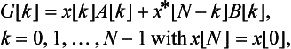
Only N points of G[k] are computed from Eq. (9.4). The remaining points are found by using the complex conjugate property of G[k], G[2N – k] = G*[k]. As a result, a 2N-point transform is calculated based on an N-point transform, leading to a reduction in the number of cycles. The codes for the functions (split1, R4DigitRevIndexTableGen, digit_reverse, and radix4) implementing this approach are provided in the TI Application Report [1].
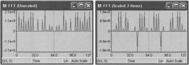
Figure 9-9 shows the FFT outcome where the signal has been scaled down 0, 2, 4, and 5 times, respectively. The scaling is done to get rid of overflows, which are present for the scale factors 0, 2, and 4. As revealed by these figures, the input signal has to be scaled down five times to eliminate overflows. When the signal is scaled down five times, the expected peaks appear. The total number of cycles for this FFT is 56,383. Since this is less than the capture time available for a 128-point data frame at a sampling frequency of 8 kHz, it is expected that this algorithm would run in real-time on the DSK.
L6.3 Real-Time FFT
To perform FFT in real-time, the triple buffering program is used. A frame length of 128 is considered here. The output is observed by halting the processor through CCS. The animate feature of CCS cannot be used here since it slows down the processing and causes frames to overlap.
The following modifications are made to the triple buffering program to run the aforementioned FFT algorithm in real-time:

The wait_buffer ( ) function is modified with the appropriate function calls so that when the input buffer is full, the transform is calculated and sent out to the host through the FIFO.
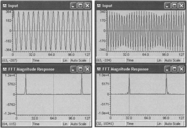
The functionality of the program can be verified by connecting a function generator to the line-in. The graphing capability of CCS can be used to plot the FFT outcome. By changing the frequency of the input, the spikes in the frequency response would move to left or right accordingly. Figure 9-10 illustrates the output for a 1 kHz and a 2 kHz sinusoidal signal. These snap shots are captured by halting the processor. The input here is scaled by shifting it right 4 bits.