Nonlinear Devices
8.1 Introduction
By exploiting the basic physics of semiconductor devices it is possible to design circuits that perform a wide variety of mathematical operations, including addition, subtraction, multiplication, and division as well as trigonometric, logarithmic, and exponential functions. Such circuits perform in the analog domain and frequently offer real advantages over more conventional digital computation. Operations where analog computation is preferable to digital include those where both the input and output signals must be analog, limited amounts of processing are required and no digital circuitry is present, the signal is differentiated to produce a rate signal, fast signals must be processed in real time, large dynamic ranges are involved, and complex or transcendental functions must be evaluated.
In an electronic design world, where a digital approach to design is preferred in many instances, much room remains for analog computation techniques, particularly in situations where a wide, dynamic range of signals or fast signals can be processed. To explain this situation, we take the case of a simple AC power meter. A simple AC power meter may be constructed very easily with a single analog multiplier as per Figure 8-1(a), where the moving coil meter can act as the integrator. A digital power meter would require conversion of both voltage and current to digital form, with considerable attention to the timing of the conversions, since the relative phase of the two signals is of critical importance. However, if with the advantage of a CPU (see Figure 8-1(b)) that has a display driven by it and a multiplexed ADC with spare capacity, the power metering facility could be added to the base system at minimal additional cost.

As another example, the first derivative of a varying analog signal is complex to calculate using digital techniques, compared to a simple C-R network for analog differentiation (Analog Devices, 1987, Section 5). Digitizing a signal with wide dynamic range also is expensive (see Figure 8-2). If such a signal is digitized with a 16-bit ADC (a comparatively expensive device), the ratio of an LSB to full scale is 96 dB; whereas if the signal were first applied to a logarithmic converter (frequently misnamed a logarithmic amplifier), then a dynamic range approaching 120 dB is practical with an 8-bit ADC.

Historically, analog computers have been slow devices. Even though high-frequency multipliers, modulators, logarithmic amplifiers, and other function generators have been available for many years, they generally have had relatively poor accuracy and stability and have not been considered analog computers. Within the last decade, a few classes of accurate nonlinear devices have entered the market: multipliers, modulators, and log amps (Analog Devices, 1990, Section 5). This chapter is an introduction to modern nonlinear devices, their design concepts, and special application areas.
8.2 A Basic Semiconductor Physics-Based Approach to Analog Computation Circuits
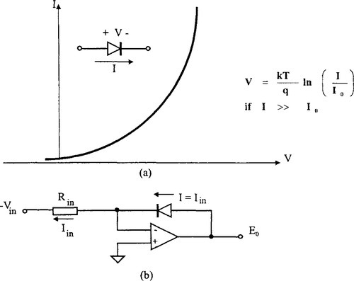
The operation of many analog computational circuits depends on the logarithmic properties of silicon junctions. An ideal logarithmic diode has the current voltage relationship
This could be rewritten as
where
I = the current through the diode;
k = Boltzman’s constant (1.38062 × 10⁻²³);
V = the voltage across the diode;
q = a constant equal to unit charge, 1.60219 × 10− 19 coulombs;
T = the absolute temperature in Kelvin;
I0 = the extrapolated current for E0 = V = 0 volts.
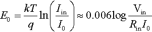
Referring to Figure 8-3, these equations clearly show that the current in a diode increases exponentially with voltage or, conversely, the voltage increases logarithmically with current. These equations are less clear in showing that I0, the theoretical diode current at zero voltage, is temperature dependent and so the variation of a diode’s behavior with temperature is by no means as simple as the equation would suggest; that is, the voltage is not proportional to absolute temperature at a fixed current. Several approximations concerning the logarithmic behavior of diodes are worth remembering:
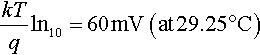
These approximations simplify the diode expression to

This simply says that V increases by 60 mV every time the current increases by a factor of 10 at 29.25°C.
If we were to place an ideal logarithmic diode in the feedback path (output to inverting input) of an operational amplifier and apply a current to the inverting input, the output voltage would be the logarithm of the input current times a temperature varying constant. For the circuit in Figure 8-3(b), if Iin ![]() I0,
I0,
It is unfortunate that real diodes are not ideal logarithmic diodes. In a real diode, the bulk resistivity, RB, of the silicon limits the logarithmic accuracy at high currents and diffusion currents in surface inversion layers and generation-recombination effects in space-charge regions cause a scale factor error, m, at low currents. We therefore find that
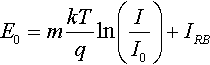
where m varies with the current.
Even with similar diodes, m can vary (it is never less than 1 and may be as high as 4), as does the value of E0 at which m changes. General purpose diodes therefore are impractical as logarithmic diodes for dynamic ranges of more than 100:1 (two decades).
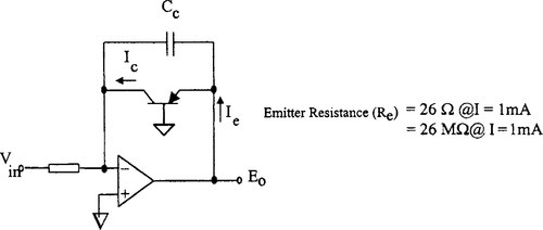
Luckily, we can replace the diode with a grounded-base transistor as per Figure 8-4 and get a dynamic range of 1 million:1 (six decades) or more — the only disadvantage of such a circuit is that the signals can have only a single polarity.

From the Ebers and Moll equations (see Sheingold, 1976, for a detailed derivation), it may be shown that
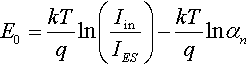
where Iin ![]() IES; IES is the emitter saturation current; and αn is the forward current-transfer ratio (αn is not the grounded-base current gain).
IES; IES is the emitter saturation current; and αn is the forward current-transfer ratio (αn is not the grounded-base current gain).
Since IES is less than a picoampere and αn is nearly unity over a wide range of currents, in the silicon planar transistors used to manufacture logarithmic converters, the effect of the second term generally may be disregarded; and the equation simplifies to
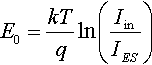
Such logarithmic converters are temperature sensitive. In equation (8.9), kT/q has a temperature coefficient of 0.34%/°C around 25°C, and IES doubles for every 10°C temperature rise and varies with device size and geometry. Many of these basic concepts, in refined forms or in combination with other compensation circuits, are used in nonlinear circuits. (For a further discussion on these basic techniques, see Devices, 1987 Sheingold 1976.)
8.3 Important Design Considerations in Nonlinear Devices
In the discussion of nonlinear devices two important design considerations are the dynamic range of a signal and the noise.
8.3.1 Dynamic Range
In many cases, a wide dynamic range is an essential aspect of a signal, something to be preserved at all costs. This is true, for example, in the high-quality reproduction of music and communication systems. However, often the signal must be compressed to a smaller range with no significant loss of information. Compression is used in magnetic recording, where the upper end of the dynamic range is limited by tape saturation and the lower end by the granularity of the medium. In professional noise-reduction systems, compression is “undone” by precisely matched nonlinear expansion during reproduction. Similar techniques are used in conveying speech over noisy channels, where the performance more likely is to be measured in terms of word intelligibility than audio fidelity. The reciprocal processes of compressing and expanding are implemented using “compandors,” and many schemes have been devised to achieve this function. In terms of the signal voltage,
Note that in a linear-impedance system, the power is proportional to the signal voltage (or current) squared. Accordingly,

Also, it is useful to differentiate between the dynamic range of the signal and that of the processing system. The signal dynamic range is

whereas the system dynamic range is

In system design, one should be concerned with the system’s dynamic range, which should match or exceed the signal dynamic range.
8.3.2 Noise Limitations
The dynamic range of all signal-processing systems is limited by random noise, which sets a fundamental bound on the smallest signal that can be detected or otherwise utilized with an adequate signal-to-noise ratio (SNR). This noise may be generated by numerous mechanisms, including those associated with the source itself (e.g., antenna, photomultiplier, piezoelectric transducer) as well as by the active and passive devices in the amplifiers.
Noise cannot be discussed without reference to bandwidth, which will be unavoidably limited by the types of amplifier used. Deliberate filtering often is included in a signal-processing channel to reduce noise, as well as to improve the separation of wanted from unwanted signals. This may take the form of bandpass, low-pass, or high-pass functions or combinations of these, depending on the situation. Nonlinear filtering also may be used, for example, to minimize the disturbance of the signal path in the presence of impulsive noise.
The noise powers of uncorrelated sources add up, so noise voltages (or currents) must be added using a root-sum-of-squares (RSS) calculation. This leads to some rather startling consequences. Suppose a system has a major voltage noise source of magnitude Ea and several minor noise sources whose RSS sum to a magnitude of Eb. Then, Ea needs to be only twice Eb for the major source to contribute almost 90% of the total system noise. When Ea/Eb = 5, 98% of the noise is due to Ea.
It follows that the overall noise performance of a practical system can benefit greatly by (i) minimizing the input-referred noise of the first stage and (ii) using the highest possible gain in this stage. However, the second of these objectives frequently cannot be realized in systems that must handle signals of a large dynamic range, because the high gain would preclude distortion-free operation at maximum signal levels.
Noise frequently is specified in terms of a noise spectral density (NSD). The term reflects the fact that the total noise power is directly proportional to the system’s noise bandwidth, BN (in Hertz). The NSD therefore usually is of interest in specifying a channel’s input-noise limitations. Note that, in general, the noise bandwidth is not equal to the −3dB bandwidth. BN can be viewed as the bandwidth of an equivalent system with a “brick-wall” cessation of response at that frequency. A system with a single-pole low-pass corner at f0 = 1/2πT has a BN value equal to π f 0/2, or 1.57 f 0, while for two such real pole low-pass sections in cascade, BN is π f 0/4 (see Figure 8-5). The total NSD will have both voltage and current components. Since the noise power is proportional to the square of either the voltage or current, these two noise components have the dimensions of volts![]() and amps/
and amps/![]() .
.

Noise signals usually are small, and therefore nonlinear effects often are negligible. In such circumstances, it is permissible to use superposition methods to evaluate each contributing source independently, followed by an RSS calculation to calculate the total noise. A notable exception is the logarithmic amplifier, where even very small noise voltages at the input can cause heavy limiting in later stages in the amplifier. Special approaches to both noise analysis and noise specification are required in such cases.
For details on noise performance, see Analog Devices, Inc. Devices (1992a) and Section 2.3.2 of Chapter 2. While noise limits the low end of a system’s dynamic range, performance at the upper end of signal range is degraded by the increasing importance of nonlinear aspects of circuit behavior.
8.4 Logarithmic Converters
The conversion of a signal to its equivalent logarithmic value involves a nonlinear operation, the consequences of which can be confusing if not fully understood. It is important to realize that many of the familiar concepts of linear circuits are irrelevant to log amps. For example, the incremental gain of an ideal log amp approaches infinity as the input tends to 0, and change of offset at the output of a log amp is equivalent to a change of amplitude at its input, not a change of input offset. The commonly used term logarithmic amplifier is something of a misnomer but is used lavishly.
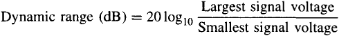
If we consider the equation y = log(x), as shown in Figure 8-6(a), every time x is multiplied by a constant A, y increases by another constant A1. Thus, if log(K) = K1 then log(AK) = K1+ A1; log(A2K) = K1 + 2A1; log(K/A) = K1 – A1. As shown in figure 8.6(a) when x is 1, y approaches 0.
A practical log amp has the graph of transfer characteristics shown in Figure 8-6(b). Such a practical log amp has the transfer function
This is valid over some range of input values, which may vary from 100:1 (40 dB) to over 1 million:1 (120 dB). The scale of the horizontal axis (the input) is logarithmic, and the ideal transfer characteristic is a straight line. When Vin = Vx, the logarithm is 0 (log 1 = 0). Vx therefore is known as the intercept voltage of the log amp, because the graph crosses the horizontal axis at this value of Vin.
With inputs very close to 0, log amps cease to behave logarithmically and most then follow a linear Vin/Vout law. This behavior often is lost in device noise. Noise often limits the dynamic range of a log amp. The constant Vy has the dimensions of voltage, because the output is a voltage. The input, Vin, is divided by a voltage, Vx, because the argument of a logarithm must be a simple dimensionless ratio.
8.4.1 Practical Log Amps and Negative Values of x
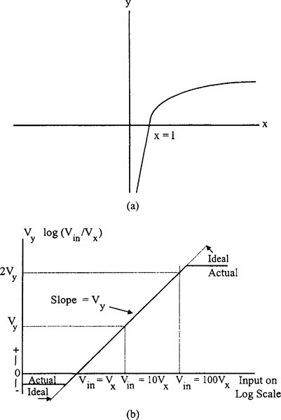
The logarithm function is indeterminate for negative values of x. Log amps can respond to negative inputs in three different ways:
1. They can give a full-scale negative output as shown in Figure 8-7(a). This basic log amp saturates with negative inputs.
2. They can give an output proportional to the log of the absolute value of the Input and disregard its sign, as shown in Figure 8-7(b). This type of log amp can be considered a full-wave detector with a logarithmic characteristic and often is referred to as a detecting log amp.
3. They can give an output proportional to the log of the absolute value of the input and have the same sign as the input, as shown in Figure 8-7(c). This type of log amp can be considered a video amp with a logarithmic characteristic and may be known as a logarithmic video (log video) amplifier or, sometimes, a true log amp.
8.4.2 Practical Implementation
Three basic architectures are used by manufacturers such as Analog Devices, Inc.: the basic diode log amp, the true log amp, and the successive detection log amp.
8.4.2.1 The Basic Diode Log Amp
As per the discussion in Section 8.2, a simple diode could be used for a log amp function (see Figure 8-3). In practice, the dynamic range of this configuration is limited to 40–60 dB because of nonideal characteristics of the diode. However, if the diode is replaced with a diode connected transistor, as shown in Figure 8-4, the dynamic range can be extended to 120 dB or more. This type of log amp has three disadvantages: both the slope and intercept are temperature dependent, it will handle only unipolar signals, and its bandwidth is both limited and dependent on the signal amplitude. Where several such log amps are used on a single chip to produce an analog computer that performs both log and antilog operations, the temperature variation in the log operations is unimportant, since it is compensated for by a similar variation in the antilogging. An example of a practical device that utilizes such techniques is the AD-538 analog computation unit (ACU) from Analog Devices, Inc. (Figure 8-8). This device, which has a transfer function of Vout, = Vy(Vz/Vx) can multiply, divide, and raise to powers. When actual logging is required, these types of devices require temperature compensation (Sheingold, 1976).

A major disadvantage of this type of log amp for high-frequency applications is its limited frequency response, limited by Miller capacitance or the residual feedback capacitance of these devices (Analog Devices, Inc., 1995). Practical limits are within a few hundred kHz. Therefore, for high-frequency applications detecting and true log architectures are used.
8.4.2.2 True and Detecting Log Amps
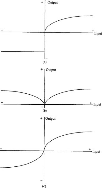
Although these two types differ in detail, the general principle behind their design is the same: Instead of one amplifier having a logarithmic characteristic, these designs use a number of similar, cascaded linear stages having well-defined large signal behavior.
As shown in Figure 8-9(a) consider N cascaded limiting amplifiers, the output of each driving a summing circuit as well as the next stage. If each amplifier has a gain of A dB, the small signal gain of the strip is NA dB. If the input signal is small enough for the last stage not to limit, the output of the summing amplifier will be dominated by the output of the last stage. As the input signal increases, the last stage will limit. It now will make a fixed contribution to the output of the summing amplifier, but the incremental gain to the summing amplifier will drop to (N − 1)A dB. As the input continues to increase, this stage in turn will limit and make a fixed contribution to the output, and the incremental gain will drop to (N− 2)A dB, and so forth, until the first stage limits and the output ceases to change with increasing signal input.
The response curve therefore is a set of straight lines, as shown in Figure 8-9(b). The total of these lines, though, is a very good approximation to a logarithmic curve and, in practice, is an even better one, because few limiting amplifiers, especially high-frequency ones, limit quite as abruptly as this model assumes. Due to the compromise needed between log approximation and number of gain stages, gains of 10–12 dB are chosen in practical devices (Analog Devices, 1995).
This general model, which is ideal, becomes difficult to implement at high frequencies due to delays associated with each stage. If each stage has a delay of t ns, a signal that passes through all stages will have a delay of Nt ns compared to a signal that passes only one stage, which is delayed by only t ns. Some solutions for such difficulties are discussed in Analog Devices (1995). Multistage architectures such as these or their variations are video log amps or true log amps. However, the most common types of high-frequency log amps are the devices based on successive detection architecture.
8.4.2.3 Successive Detection Log Amps
The successive detection log amp consists of cascaded limiting stages as described previously, but instead of summing their outputs directly, these outputs are applied to detectors, and the detector outputs are summed as shown in Figure 8-10. If the detectors have current outputs, the summing process may involve no more than connecting all the detector outputs.

Log amps using this architecture have two types of output: the log output and a limiting output. In many applications, the limiting output is not used, but in some (FM receivers with “S” meters, for example) both are necessary. The log output of a successive detection log amplifier generally contains amplitude information, and the phase and frequency information is lost.
In the past, it has been necessary to construct high-performance, high-frequency successive detection log amps using a number of individual limiting amplifiers. These typically are assembled in complex and costly hybrids. Recent advances in IC processes have allowed this complete function to be integrated on a single chip.
The AD-640 log amp from Analog Devices is an example of successive detection type log amp for high-frequency use. The AD-640 log amp contains five limiting stages (10 dB per stage) and five full-wave detectors in a single IC package, and its logarithmic performance extends from DC to 145 MHz. A block diagram of AD-640 is shown in Figure 8-11.

With reference to Figure 8-11(b), the AD-640 has its log amp transfer function where Vx is calibrated to 1 mV exactly. The slope of the line is directly proportional to Vy. Base 10 logarithms are used in this context to simplify the relationship to decibel values. For Vin = 10Vx, the logarithm has a value of 1, so the output voltage is Vy. At Vin = 100Vx, the output is 2Vy, and so on. Vy therefore can be viewed either as the slope voltage or as the volts per decade factor.
The AD-640 conforms to equation (8.1) except that its two outputs are in the form of current rather than voltage:
Each of the five stages in the AD-640 has a gain of 10 dB and a full-wave detected output. The transfer function of the device is shown in Figure 8-11(b) along with the error curve. Note the excellent log linearity over an input range of 1–100 mV (40 dB). Although well suited to RF applications, the AD-640 is DC coupled throughout. This allows it to be used in low-frequency and very low-frequency systems, including audio measurements, sonar, and other instruments requiring operation to low frequencies or even DC. Unlike many other log amps, the AD-640 is laser trimmed to a high absolute accuracy of both slope and intercept and is fully temperature compensated. Some key features of the AD-640 are
1. 45 dB dynamic range, two can cascade to 95 dB.
2. Bandwidth DC to 145 MHz (120 MHz when cascaded).
3. Slope of 1 mA/decade, temperature stable.
4. Less than 1 dB log nonlinearity.
5. Balanced circuitry for stability and minimal external components.
For further details on applications, see Analog Devices (1992a, 1992c, 1995).
8.4.3 Key Parameters of Log Amps and Classifications
In selecting log amps for a given application, key parameters to be considered are listed in Table 8-1.
Table 8-1
Key parameters of log amps
| Parameter | Description |
| Noise | Noise referred to the input (RTI) of the log amp, which may be expressed as a noise figure, as noise spectral density (voltage, current, or both), or as noise voltage (or noise current or both) |
| Dynamic range | Range of signal over which the amplifier behaves in a logarithmic manner (expressed in decibels) |
| Frequency response | Range of frequencies over which the log amp functions correctly |
| Slope | Gradient of transfer characteristic in V/dB or mA/dB |
| Intercept point | Value of input signal at which output is 0 |
| Log linearity | Deviation of transfer characteristic (plotted on log/line axes) from a straight line (expressed in decibels) |
Over the years, logarithmic amplifiers have accumulated a confusing assortment of terms, some quite misleading. Here (Table 8-2), Analog Devices, Inc. attempts to classify log amps into three broad groups according to structure and application domain and try to be consistent in matters of terminology and nomenclature. For details, see Analog Devices (1992a, Section 9).
Table 8-2
Types of log amps and their behavior.
| Type | Performance |
| Translinear log amps | Based on logarithmic (or translinear) properties of bipolar transistors; wide dynamic range, poor AC performance |
| Baseband log amps | Respond to instantaneous value of rapidly changing input, “progressive compression technique” often used, sometimes called video log amps, “true log amp” accepts bipolar inputs sign of output following input |
| Demodulating log amps | AC input signal is rectified, output is the modulated envelope of the input, often called successive detection log amp |
(Reproduced by permission of Analog Devices, Inc.)
8.5 Multipliers and Dividers
A multiplier is a device having two input ports and an output port. The signal at the output is the product of the two input signals. If both input and output signals are voltages, the transfer characteristic is the product of the two voltages divided by a scaling factor, K, which has the dimension of voltage (see Figure 8-12(a)). From a mathematical point of view, multiplication is a four-quadrant operation; that is to say, both inputs may be either positive or negative, as may be the output. Some of the circuits used to produce electronic multipliers, however, are limited to signals of one polarity. If both signals must be unipolar, we have a single-quadrant multiplier and the output also is unipolar. If one of the signals is unipolar, but the other may have either polarity, the multiplier is a two-quadrant multiplier and the output may have either polarity (and is bipolar). The circuitry used to produce one- and two-quadrant multipliers may be simpler than that required for four quadrant multipliers; and since in many applications full four-quadrant multiplication is not required, it is common to find accurate devices that work only in one or two quadrants.

Many techniques can be used for analog multipliers, and some of these are discussed in Sheingold (1976). Most common forms are the use of log/antilog circuits or the use of a Gilbert cell (Gilbert, 1968a, 1968b). The AD-538 from Analog Devices is such a monolithic integrated circuit (Figure 8-8).
Some disadvantages of such circuits are its unipolar inputs and the variation of its bandwidth with the signal amplitude. The problem of bandwidth variation arises from the variation of emitter resistance, RE, with current in the grounded-base transistor. With reference to Figure 8-13, RE is inversely proportional to the emitter current, being approximately 26 Ω at 1 mA. The bandwidth of the circuit is inversely proportional to the product of RECC (CC may be an external compensation capacitor or merely stray capacitance) and thus is proportional to the transistor current. Therefore, if the logarithmic converter works over a 120 dB dynamic range, its bandwidth will vary by 1 million: 1, which can be inconvenient. For details, see Analog Devices (1987).
In addition to adopting other improved logarithmic conversion techniques, a popular technique used in commercial analog multiplier ICs is the Gilbert cell. There is a linear relationship between the collector current of a silicon junction transistor and its transconductance (gain) that is given by the following equation:
where
VBE = base-emitter voltage;
q = electron charge (1.60219 × 10− 19);
k = Boltzmann’s constant (1.38062 × 10− 23);
q/kT = 1/(25.69 mV) at 25°C.
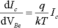
This relationship may be exploited to construct a multiplier with a long-tailed pair of silicon transistors (Analog Devices, 1987), as shown in Figure 8-14. At 25°C, this circuit provides an output of q/kT[(Vy + VBE)/(4.7 × 103)] (10/10,010)Vx for the case of Icl − Ic2 = ∆Ic.
However, this is a rather poor multiplier because
1. The y input is offset by the VBE, which changes nonlinearly with Vy.
2. The x input is nonlinear as a result of the exponential relationship between Ic and VBE.
3. The scale factor varies with temperature.
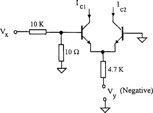
Gilbert realized that this circuit could be linearized and made temperature stable by working with currents rather than voltages and by exploiting the logarithmic properties of transistors, as per the case shown in Figure 8-15(a).
The x input to the Gilbert cell takes the form of a differential current, and the y input is a unipolar current. The differential x currents flow in two diode-connected transistors, and the logarithmic voltages compensate for the exponential VBE/Ic relationship. Furthermore, the q/kT scale factors cancel each other. This gives the Gilbert cell the linear transfer function for Ic = (Ic1 − Ic2):
As it stands, the basic Gilbert cell shown in Figure 8-15(a) has three inconvenient features:
1. Its x input is a differential current.
2. Its output is a differential current.
3. Its y input is a unipolar current.
This makes the cell a two-quadrant multiplier.
By cross-coupling two such cells and using two voltage-to-current converters (as shown in Figure 8-15(b)), we can convert the basic architecture to a four-quadrant device with voltage inputs. A practical example of this type of a multiplier is the AD-534 from Analog Devices. In Figure 8-15(b), Q1A and Q1B and Q2A and Q2B form the two core long-tailed pairs of the two Gilbert cells, while Q3A and Q3B are the linearizing transistors for both cells. Figure 8-15(b) shows an operational amplifier acting as a differential current to single-ended voltage converter; but for higher speed applications, the cross-coupled collectors of Q1 and Q2 form a differential open collector current output (as in the AD-834 multiplier with a 500 MHz range). Motorola’s MC 1494 and 1495 are other examples of four-quadrant multipliers.
A basic wideband multiplier using the AD-834 (for 500 MHz bandwidth) is shown in Figure 8-16(a). Figure 8-16(b) indicates the block diagram of a 10 MHz multiplier with direct-divide capability.

For details on multipliers, see Analog Devices (1995, Section 3).
8.6 RMS-to-DC Converters
The root mean square (RMS) is a fundamental measurement of the magnitude of an AC signal. Defined practically, the RMS value assigned to the AC signal is the amount of DC required to produce an equivalent amount of heat in the same load. Defined mathematically, the RMS value of a voltage is the value obtained by squaring the signal, taking the average, and then taking the square root. The averaging time must be sufficiently long to allow filtering at the lowest frequencies of operation desired. A complete discussion of RMS-to-DC converters can be found in Kitchen and Counts (1986) and application of these in multimeters are discussed in Kularatna (1996). Two basic techniques are used in RMS-to-DC converters: explicit and implicit.
8.6.1 Explicit Method
The explicit method is shown in Figure 8-17(a). The input signal is first squared by a multiplier. The average value is taken by using an appropriate filter, and the square root is taken using an op amp with a second squarer in the feedback loop. This circuit has limited dynamic range because the stages following the squarer must try to deal with a signal that varies enormously in amplitude. This restricts the method to inputs with a maximum dynamic range of approximately 10:1 (20 dB). However, excellent bandwidth (greater than 100 MHz) can be achieved with high accuracy if a multiplier such as the AD-834 is used as a building block (see Figure 8-17(b)).

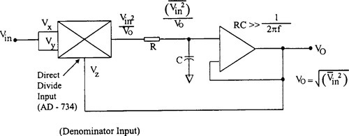
8.6.2 Implicit Method
Figure 8-18 shows the circuit for computing the RMS value of a signal using the implicit method. Here, the output is fed back to the direct-divide input of a multiplier such as the AD-734. In this circuit, the output of the multiplier varies linearly (instead of as the square) with the RMS value of the input. This considerably increases the dynamic range of the implicit circuit as compared to the explicit circuit. The disadvantage of this approach is that it generally has less bandwidth than the explicit computation.
8.6.3 Monolithic RMS/DC Converters
While it is possible to construct such an RMS circuit from an AD-734, it is far simpler to design a dedicated RMS circuit. The Vin2/Vz circuit may be current driven and only one quadrant if the input first passes through an absolute value circuit. Figure 8-19(a) shows a block diagram of a typical monolithic RMS/DC converter such as the AD-536. It is subdivided into four major sections: absolute value circuit (active rectifier), squarer/divider, current mirror, and buffer amplifier. The input voltage, Vin, which can be AC or DC, is converted to a unipolar current, Iin, by an absolute value circuit. Iin drives one input of the one-quadrant squarer/divider, which has the transfer function Iin2/If. The output current, Iin2/If, of the squarer/divider drives the current mirror through a low-pass filter formed by R1 and an externally connected capacitor, CAV. If the R1CAV time constant is much greater than the longest period of the input signal, then Iin2/If is effectively averaged. The current mirror returns a current, If, that equals the average value of ![]() back to the squarer/divider to complete the implicit RMS computation. Therefore,
back to the squarer/divider to complete the implicit RMS computation. Therefore,
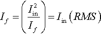

The current mirror also produces the output current, Iout, which equals 2I f. The circuit provides a decibel output also, which has a temperature coefficient of approximately 3300 ppm/°C and must be temperature compensated.
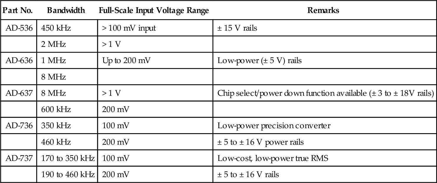
There are a number of RMS/DC converters in monolithic form. A representative list from Analog Devices is shown in Table 8-3. For practical applications, design details, and selection of RMS/DC converters, see Analog Devices (1992c, 1995), Kitchen and Counts (1986), and Kularatna (1996).
Table 8-3
A representative set of RMS/DC converters from Analog Devices, Inc.
| Part No. | Bandwidth | Full-Scale Input Voltage Range | Remarks |
| AD-536 | 450 kHz | > 100 mV input | ± 15 V rails |
| 2 MHz | > 1 V | ||
| AD-636 | 1 MHz | Up to 200 mV | Low-power (± 5 V) rails |
| 8 MHz | |||
| AD-637 | 8 MHz | > 1 V | Chip select/power down function available (± 3 to ± 18V rails) |
| 600 kHz | 200 mV | ||
| AD-736 | 350 kHz | 100 mV | Low-power precision converter |
| 460 kHz | 200 mV | ± 5 to ± 16 V power rails | |
| AD-737 | 170 to 350 kHz | 100 mV | Low-cost, low-power true RMS |
| 190 to 460 kHz | 200 mV | ± 5 to ± 16 V rails |
8.7 Function Generators
Some interesting applications of nonlinear devices involve function generation using AD-538-type devices and AD-639 trigonometric function generators. To fully appreciate these devices, keep in mind that some digital techniques such as direct digital synthesis (DDS) still have restrictions at high frequencies, beyond several megahertz. An example of these could be shown using the AD-538. The arc-tangent circuit shown in Figure 8-20(a) is typical of AD-538 applications where Y is 1 so that Vo = (Z/X)M for M < 1.

In an approximation to the arc-tangent function, the AD-538 may be made to compute the angle represented by two rectangular coordinates, which, since they are applied to the X and Z inputs, we shall call X and Z rather than the more usual X and Y. If X and Z are within the range 100 μV to 10 V, the error in the computed angle is under 1° (the AD-639 can perform a similar computation with fewer components but cannot work over a wide dynamic range).
The circuit exploits the fact that

where T is the angle normalized to 90°.
The AD-538 and the external amplifier calculate log(tan T) from X and Z, amplifie it by a factor of 1.21 to raise to the 1.21 power, and perform an implicit calculation to calculate the angle (which is expressed in terms of the reference voltage). Under these conditions, the output voltage tends to VREF as the angle tends to 90° although, in fact, the circuit cannot be used much above 89.5° because at 90° tangents become infinite and before that the circuit becomes unstable. R1 and R2 must be matched for highest accuracy, and the circuit is stabilized by the 0.1 μF integrating capacitor in the amplifier feedback path. The circuit works in a single quadrant since both X and Z must be positive.
Trigonometric functions more normally are calculated by the AD-639. No external components (other than supply decoupling capacitors) are required to compute sines, cosines, tangents and cotangents, and secants and cosecants with the AD-639. Little more than an extra reference voltage (which may be generated from the internal reference with an operational amplifier and a couple of resistors) is required for versines and coversines. For details of the less common functions, consult the AD-639 data sheet (Analog Devices, 1999) and various application notes — the sine, cosine, and tangent will be described here. Some interesting applications of the AD-639 are discussed in Analog Devices (1987).
8.8 Benistor, a Newly Introduced Device
An interesting novel component surfaced recently (Bindra, 1998) from the Bensys Corporation, the Benistor™. (The name Benistor is a combination of the company’s name and transistor.) The Benistor, which performs similar to multielectrode vacuum tubes, can independently control the voltage and current output from the device.
Introduced in 1998, the device block diagram, shown in Figure 8-21(a), comprises four blocks: the power controller (PC), the current separator (CS), the current controller (CC), and the voltage threshold controller (VTC). In the first commercial device, BEN 35100, the PC is a simple PNP transistor that acts as a switch or a variable resistor between the power source and the load. The CS block incorporates three NPN transistors to enable the voltage controller and current controller to work simultaneously or separately.

Comprising two open-collector op amps and two resistors, the current controller acts as a voltage/current converter for the power controller. There are two control inputs to this block: the noninverting input CC and the inverting input ![]() . The amount of voltage input at the noninverting current control is directly proportional to the current output to the load, and the amount of voltage at the inverting electrode is inversely proportional to the output current. Functioning as a window comparator, the VTC controls the buffer’s base current, in either a switching or self-switching mode. The two controls of the VTC are effective voltage control (EVC) and maximum voltage control (MVC), which determine the threshold voltages of the output. While the voltage at the EVC establishes the threshold for switching from off to on, the voltage at MVC pin determines the on/off states. In effect, the voltage settings on these two pins pre-establish the output voltage window.
. The amount of voltage input at the noninverting current control is directly proportional to the current output to the load, and the amount of voltage at the inverting electrode is inversely proportional to the output current. Functioning as a window comparator, the VTC controls the buffer’s base current, in either a switching or self-switching mode. The two controls of the VTC are effective voltage control (EVC) and maximum voltage control (MVC), which determine the threshold voltages of the output. While the voltage at the EVC establishes the threshold for switching from off to on, the voltage at MVC pin determines the on/off states. In effect, the voltage settings on these two pins pre-establish the output voltage window.
In summary, the Benistor is a multielectrode device consisting of impedance command pins for precise control of output current and voltage. Consequently, eight electrodes completely define the Benistor. These are shown in Figure 8-21(b).
The SS electrode (not used in the BEN 35100 version) sets the initial state of the Benistor’s self-switching mode of operation as either on or off at the beginning of an input power pulse wave. Having only two states, it is either grounded (on) or floating (off). Likewise, the CE provides the reference voltage for the device, while the CC determines the window of output current, and the VTC pre-establishes the window of output voltage. Based on these settings, the power controller will deliver to the load only that part of the input power signal, with respect to the amount of current and voltage, within the two pre-established ranges. In effect, together, the voltage and current-control electrodes can provide the system designer virtually any output possibility.
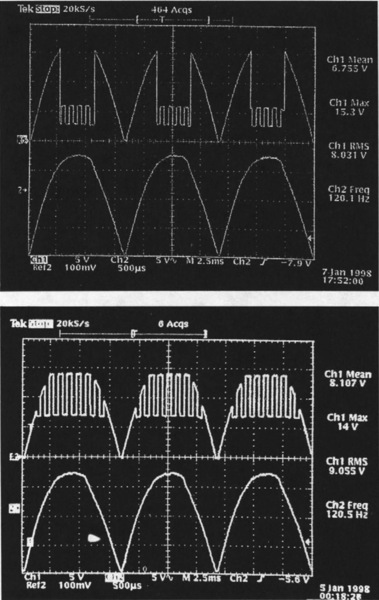
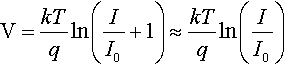
Because the device can accept AC, DC, and pulse input and provide output in any of these modes or any combination (based on conditions at the control electrodes), the Benistor inspires a new way of thinking in power control and power conversion. Combining the capability of all three previous values, it provides designers a unique method of controlling power parameters. Figure 8-22 indicates complex waveforms that can be obtained from the same input (bottom traces). For further details, see Bindra (1998), and Bensys Corporation (•••, •••, •••, •••) and U.S. Patent No. 5,598,093.