
Operational Amplifiers
2.1 Introduction
The world is analog. With the invention of the transistor, electronics engineers gained competence in the digital processing of analog signals. However, in all signal processing systems, designers have to receive, amplify or attenuate, or process the analog signals using varieties of analog techniques. The operational amplifier (op amp) is one of most commonly used analog components for such tasks.
Bob Widlar, working at Fairchild, designed the first successful op amp back in 1965. The first commercial monolithic device was μA709. The developments that continued from this experience provided several successful op amps, such as the μA741 and the LM301. With advancements in semiconductor manufacturing technologies, many advanced op amps entered the market. Today op amps are available in a wide variety of technologies, specifications, prices, and package styles from a multitude of vendors. When a circuit requires an op amp, the designer is confronted with a bewildering number of devices from which to choose. These varieties may be identified as basic voltage feedback, current feedback, micro-power, video, and chopper stabilized types.
This chapter provides a designer’s viewpoint on the use of op amps, identifying their characteristics and limitations in a practical sense and discussing the use of different kinds. Many excellent references (Horowitz and Hill, 1996; Analog Devices, 1987, 1990, 1992, 1995; Dostal, 1993) support this chapter with more detailed fundamentals.
2.2 Introduction to Amplifiers
There are four general classes of amplifiers, characterized by transfer characteristics expressed in volts per volt, amperes per ampere, volts per ampere, and amperes per volt. These four cases are illustrated in Figure 2-1.
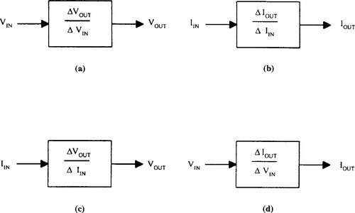
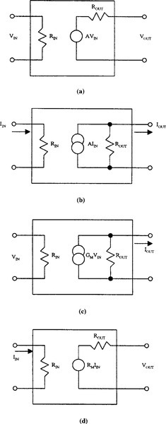
These basic amplifiers are the building blocks required to synthesize larger electronic systems. Although some simple electronic devices are voltage amplifiers (the triode vacuum tube), current amplifiers (the bipolar transistor), and transconductance amplifiers (the field effect transistor), presently no electronic devices demonstrate the intrinsic characteristics of a transimpedance amplifier. Hence transimpedance amplifiers. must be synthesized from voltage, current, or transconductance amplifiers. Characteristics of the ideal amplifiers are shown in Table 2-1 and the amplifier equivalent circuits are shown in Figure 2-2.
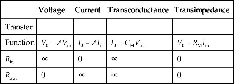
Table 2-1
Ideal Amplifier Characteristics
| Voltage | Current | Transconductance | Transimpedance | |
| Transfer | ||||
| Function | V0 = AVin | I0 = AIin | I0 = GMVin | V0 = RMIin |
| Rin | ∝ | 0 | ∝ | 0 |
| Rout | 0 | ∝ | ∝ | 0 |
2.3 Basic Operational Amplifier
The ideal op amp has differential inputs, an infinite input impedance, a single-ended output, and infinite gain at all frequencies. The ideal op amp always must be considered as a four-terminal device, the fourth terminal being the return path for the output current. In most designs, it is assumed that the amplifier is ideal and that no current flows into the input terminals, there is no input offset voltage, and no power is required for its operation. Figure 2-3 shows the ideal op amp.

2.3.1 The Real Operational Amplifier
Figure 2-4 depicts a real op amp based on a voltage amplifier. Let us briefly discuss the input imperfections and output obstacles.
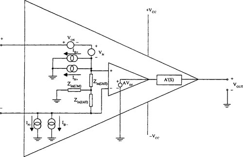
2.3.1.1 Input Imperfections
The actual characteristics of real op amps are considerably more complicated. Each input contains a DC current source (IB, the bias current), and a DC voltage source (Vos, the offset voltage) in series with the inputs. The amplifier has differential and common mode input impedances (Zin(DIFF) and Zin(CM), respectively), which usually are complex and consist of a resistor and a capacitor in parallel.
Also, there are three uncorrelated noise sources: two current sources (IN) and a voltage source (VN) that appear differentially. Finally, the amplifier has gain with regard to common mode signals, which the ideal amplifier does not have, and so its common mode rejection ratio (CMRR) needs to be specified.
2.3.1.2 Output Stage
The output side of the model also is not ideal. There is an output impedance (Ro) in series with the voltage sources. The gain (A, infinite in the ideal model) is both finite and a function of frequency in a real amplifier, which also has a finite slew rate (the rate of rise of output voltage per microsecond) and limited output voltage and current capabilities.
2.3.1.3 Differential to Single-Ended Conversion
One fundamental requirement of a simple op amp is that an applied signal, which is fully differential at the input, must be converted to a single-ended output; that is, with respect to the often neglected fourth terminal. To see how this can lead to difficulties, look at Figure 2-5. The signal flow illustrated by Figure 2-5 is used in several popular integrated circuit families, such as the 101, 741, 748, 503, and other integrated circuit amplifiers.
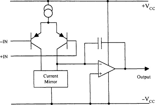
The circuit first transforms a differential input voltage into a differential current. This input stage function is represented by PNP transistors in Figure 2-5. The current then is converted from differential to single-ended form by a current mirror connected to the negative supply rail. The output from the current mirror drives a voltage amplifier and power output stage, which is connected as an integrator. The integrator controls the open-loop frequency response, and its capacitor may be added externally, as in the 101, or self-contained, as in the 741. Most descriptions of this simplified model do not emphasize that the integrator has a differential input, of course. It is biased positive by a couple of base-emitter voltages, but the noninverting integrator input is referred to the negative supply.
It should be apparent that most of the voltage difference between the amplifier output and the negative supply appears across the compensation capacitor. If the negative supply voltage is changed abruptly, the integrator amplifier will force the output to follow the change. When the entire amplifier is in a closed-loop configuration the resulting error signal at its input will tend to restore the output, but the recovery will be limited by the slew rate of the amplifier. As a result, an amplifier of this type may have outstanding low-frequency power supply rejection, but the negative supply rejection is fundamentally limited at high frequencies. Since the feedback signal to the input causes restoration of the output, the negative supply rejection will approach 0 for signals at frequencies above the closed-loop bandwidth. This means that high-speed, high-level circuits can “talk” to low-level circuits through the common impedance of the negative supply line. This phenomenon demands some special consideration in decoupling and grounding; details are discussed in Brokraw (Analog Devices, AN-202).
2.3.2 Amplifier Specifications
2.3.2.1 Offset Voltage
Offset voltage (Vos) is defined as the voltage that must be applied to the input to cause the output to be 0. Offset voltage is the result of a mismatch in the base-emitter voltages of the differential input transistors (the gate-source voltage mismatch in FET-input amplifiers) and is indistinguishable from a DC input signal. This offset can be trimmed to 0 with a potentiometer, which adjusts the balance of the operating currents in the input stage until VBE1 and VBE2 (or VGS1 and VGS2) are equal. Even if the offset voltage is trimmed to 0 at one particular temperature, it will vary with the temperature. When a bipolar transistor op amp is trimmed for minimum offset, it is trimmed for minimum temperature drift, but this is not the case for FET-input op amps.
2.3.2.2 Input Bias Current
Another DC parameter of op amps is input bias current (IB). If an op amp uses bipolar transistors in its input stage, a base current must be supplied from somewhere to bias them into their active operating region. Since Kirchhoff’s law tells us that current must flow in circles, this current also must return to its origin through a DC path. Therefore, operational amplifiers cannot be used with input signal sources that are not referred to the same power source as the amplifier itself. Although FETs do not require a base current, they nevertheless have a leakage current from their gate junction diode, which results in an input bias current. In many applications, the errors due to bias currents actually are less than the errors caused by the mismatch of the bias currents on the two inputs. This difference between the bias currents, called the input offset current, usually is specified along with the bias current.
Like the input offset voltage, bias currents also vary with temperature. In an amplifier with a bipolar input stage, the bias current decreases with increasing temperature because the transistors’ β increases, and since their emitter current remains constant, the base current decreases. In FET input amplifiers, the bias current is the gate leakage current of an FET, which is the leakage current of a reverse-biased junction diode. Such leakage currents double for every 10 °C rise in junction temperature.
An ideal op amp has no current going into its input terminals; real op amps approach this by reducing bias currents to femtoamp levels. As a category, one can consider low bias current op amps as those-with less than 1 nA bias currents.
2.3.2.3 Open-Loop Voltage Gain
Another op amp parameter that distinguishes a real amplifier from an ideal amplifier is the open-loop gain. The open-loop gain of an ideal op amp is assumed to be infinite. The same assumption occasionally is made of real amplifiers, with unfortunate results. Op amps generally have around 20 V of output swing and gains of over 1 million ![]() the input therefore would need to be on the order of 1 μV, and it is very hard to handle such signals without unacceptable errors due to thermoelectric potentials. Special circuits are necessary to measure the open-loop voltage gain.
the input therefore would need to be on the order of 1 μV, and it is very hard to handle such signals without unacceptable errors due to thermoelectric potentials. Special circuits are necessary to measure the open-loop voltage gain.
2.3.2.4 Frequency Response
Most operational amplifiers have a very simple frequency response. The gain is constant at DC and very low frequencies, then has a single-pole roll-off, falling at 6 dB/octave (− 20 dB/decade). It is obvious that, throughout the region where this single-pole frequency response applies, the product of gain and frequency is a constant, known as the gain-bandwidth product of the amplifier, and a measure of its high-frequency performance. In the majority of op amps, this single-pole response continues past the point where the gain has dropped to unity (such amplifiers are known as internally compensated or unity gain stable amplifiers). Some amplifiers have a more complex response, and at a gain of something less than 10, a second pole appears. These amplifiers are not stable at low-closed loop gains but generally have better high-frequency performance than the internally compensated types. Op amps are considered wideband fast settling if their bandwidth is greater than 5 MHz, they slew at more than 10 V/μs, and they settle to 0.1% in 1 μs or less.
2.3.2.5 Slew Rate
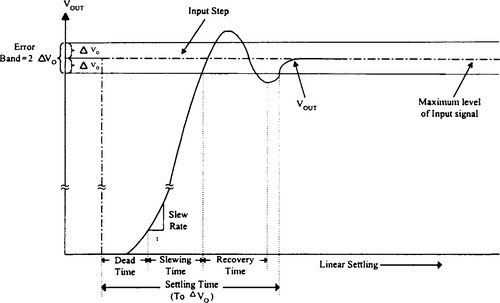
The slew rate of an amplifier is the rate at which the output voltage can change when high drive is applied to the input. When the circuit is used to measure slew rate, the input signal is a fast square wave of sufficient amplitude to drive the output of the device under test (DUT) to saturation. An oscilloscope is used to observe the slew rate of the DUT output. See Figure 2-6 for slew rate and settling time.
2.3.2.6 Common Mode Rejection Ratio
The ideal operational amplifier has only differential gain and is insensitive to the absolute voltage on the inputs. A real amplifier has several nonideal characteristics associated with input levels. First of all, the range of input voltage is limited. Few IC op amps will operate when the voltages on the input terminals are outside the supply voltages. The second, and perhaps more subtle, characteristic is the common mode rejection ratio. The CMRR is the ratio of a change in common mode voltage to the change in differential input voltage that would produce the same change in output. It often is convenient to specify this parameter in decibels.
2.3.2.7 Settling Time
Settling time is an important op amp specification, especially when the amplifier must handle rapidly changing signals. In applications such as multiplexers, sample/hold amplifiers, and amplifiers used with A/D and D/A converters, the amplifier settling time often determines the maximum data rate for a specified accuracy.
Settling time is the time that elapses between the application of a step input to the time at which the amplifier output enters, and remains within, a specified error band symmetrical to the final output value.
Settling time is determined by both linear and nonlinear characteristics of the amplifier. It varies with the input signal level and is greatly affected by impedances external to the amplifier. For these reasons, extrapolation of settling times from one set of operating conditions to another becomes virtually impossible. Settling time cannot be predicted from open-loop specifications, such as slew rate or small signal and bandwidth, as it is a closed-loop parameter. The best way to know how fast an amplifier will settle in a particular application is to measure it.
2.3.2.8 Noise
In addition to noise present on the input signal, op amp circuits have noise due to external interference and the inherent noise of the circuit itself. Interference noise originates from sources not related to the actual circuit; such noises include ground and power supply noise, stray electromagnetic pickup, contact arcing in switches and relays, and transients due to switching in reactive circuits. Even mechanical vibration can create noise in high-impedance amplifier circuits, either by piezoelectric pickup due to the use of piezoelectric plastic material in cables or circuit boards or by capacitance variation as the circuit vibrates. External interference often can be eliminated, once the interfering source is identified and appropriate action taken. The inherent noise of the op amp circuit itself cannot be totally eliminated, since it is caused by components within the circuit. The best that can be accomplished is to minimize the noise in a specific bandwidth of interest. Four types of noise are commonly encountered in operational amplifiers: popcorn noise, flicker noise, shot noise, and Johnson noise. Popcorn noise is well understood and of less importance in modern components. Flicker noise is the dominant noise at low frequencies. It has a power spectral density inversely proportional to frequency (hence the term 1/f noise). The noise voltage spectral density therefore is inversely proportional to the square root of frequency. In modern op amps, it is rarely significant above 50 Hz.
Thermal excitation of the electrons in conductors causes random movement of charge. In a resistor, this random current causes a noise voltage, known as Johnson noise, whose amplitude is given by the formula
EN(rms)=√4KTRB
where
K = Boltzman's constant (1.38 x 10 − 23 J/°K);
T = temperature (K);
R = resistance (Ohms, Ω);
B = bandwidth (Hertz).
At room temperature (25 °C), this may be simplified to
EN(rms)≈18√RB
or
en≈4√R
where
R = resistance (k Ω);
B = bandwidth (kHz);
en = spectral density (nV/ √Hz![]() ).
).
Johnson noise is a fundamental property of resistance and important in designing low-noise circuitry. It could be reduced only by reducing the temperature, the resistance, or the working bandwidth. As a reference point, it is useful to remember that at room temperature a 1 kΩ resistor has 4nV/√Hz![]() of white noise. This is equivalent to 128 nV rms noise in a 1 kHz bandwidth.
of white noise. This is equivalent to 128 nV rms noise in a 1 kHz bandwidth.
Shot, or Schottky, noise is caused by the statistical variations in the rate of electron flow; these manifest themselves as a noise current in semiconductors, where the current consists of a flow of electrons or holes. Shot noise IN is given by the formula
IN=5.7×10⁻⁴√IjB
Where
IN = noise current (picoamps rms);
Ij = junction current (picoamps);
B = bandwidth of interest.
Shot noise is important only when the operational bandwidth is large or the noise current is an appreciable factor of the total current.
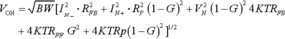
Figure 2-7 shows a generalized noise model applicable to all op amps, including current feedback types. In addition to the input noise currents and voltages, the Johnson thermal noise voltages associated with the three resistors are included.
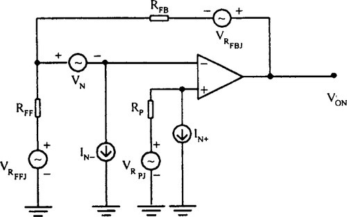
Equation (2.7) is given for calculating the effective integrated output noise voltage in a given bandwidth. The appropriate values for IN−, IN+, and VN are taken from the current and voltage noise spectral densities given on the data sheet. Usually the noninverting input noise current IN+ is neglected because the noninverting input almost always is grounded, bypassed, or driven from a low-impedance source. In making noise performance comparisons among op amps, it often is useful to convert the output noise voltage (VON) to an effective integrated input noise voltage (VIN). This is accomplished easily by dividing the integrated output noise voltage by the noise gain; that is, 1 + RFB/RFF.
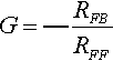
As applied to Figure 2-7, the gain of stage is
G=―RFBRFF
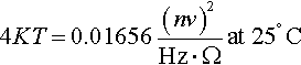
4KT=0.01656(nv)2Hz⋅Ωat25°C
VON=√BW[I2N_⋅R2FB+I2N+⋅R2P(1–G)2+V2N(1–G)24KTRFB+4KTRFFG2+4KTRp(1–G)2]1/2
Where
VON = effective integrated output noise;
VIN = effective integrated input noise;
VIN=VON1−G

Figure 2-8 shows the noise current and voltage spectral density for a practical op amp such as AD9617 from Analog Devices.
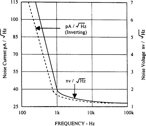
Both the noise current and noise voltage are a function of frequency but flatten out above 1 kHz, where the 1/f current noise no longer is significant. To determine the effective noise over a bandwidth where the curves are not flat, the designer must determine the areas under the respective curves for the bandwidth of interest.
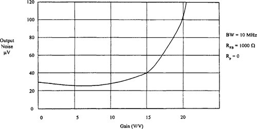
Figure 2-9 shows a plot of the effective integrated output noise for the AD844 current feedback op amp from Analog Devices. Note that, at low closed-loop gains, the predominant noise source is the input current noise that flows through the feedback resistor (1000 Ω). For closed-loop gains greater than 15, however, the effects of the “gained-up” input voltage noise begin to dominate the output noise.
Low-noise op amps can be considered those with less than 15−20nV/√Hz.![]() In the most recent low-noise devices, typical noise voltages of 2−4nV/√Hz
In the most recent low-noise devices, typical noise voltages of 2−4nV/√Hz![]() and noise currents of 2−4nΑ/√Hz
and noise currents of 2−4nΑ/√Hz![]() are common.
are common.
2.3.2.9 Linearity and Distortion
An ideal amplifier produces an exact scaled replica of its input signal at its output. To do this, the slope of its transfer characteristic must be constant. Altering the shape of the input signal between the input and the output is referred to as distorting it. Distortion is the result of processing a signal in a nonlinear system. A remarkable property of feedback amplifiers is their ability to improve linearity through the use of feedback. The actual mechanism by which this is accomplished is not obvious but may be approached by using a combination of analytical and graphic techniques.
The effect of adding feedback to improve linearity may be treated mathematically. These methods of analysis become increasingly more important as the total harmonic distortion (THD) in an amplifier is used as a criterion for selecting it.
It is clear from Figure 2-10(a) that feedback improves linearity. As per Figure 2-10(b),
VoVS=G(1+GH)=A
dAdG=1(1+GH)
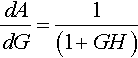
It is apparent from equation (2.10) that increasing the product GH reduces the sensitivity of the overall amplifier to a variation of G and hence reduces nonlinearity. It is difficult to discern the presence of distortion on a sinusoidal waveform visually by using an oscilloscope; our eyeballs just are not calibrated to detect slightly distorted sinusoids (it sometimes is less difficult to perceive distortion on noncurvy waveforms such as pulses and square, triangular, and sawtooth waves). The most effective means of measuring distortion is to use a spectrum analyzer and measure the harmonically related components resulting from the nonlinear characteristics of an amplifier.
The most common form of distortion is “limiting” or “clipping,” which occurs when the required output voltage from an amplifier is larger than the maximum voltage the amplifier actually can provide (the output is said to exceed the amplifier’s “headroom” or to “limit”). Symmetrical clipping introduces high levels of odd harmonics into a waveform, asymmetrical clipping introduces even harmonics as well. The cures are to either reduce the gain of the amplifier or increase its supply voltages.
Although clipping may be considered a gross form of nonlinearity, the term normally is reserved for phenomena that cause the central part of the amplifier transfer characteristic to deviate from a straight line. Consider a 12-bit system with a full-scale range of 10 V. Specifying the system to be linear to 12 bits implies that the maximum deviation from the ideal transfer curve is 1 LSB (2.44 mV).
The two most common types of nonlinearity are square law and logarithmic. Square law nonlinearity occurs when there is a quadratic term in the transfer characteristic of the amplifier and can be produced by a field effect transistor with a resistive load. Logarithmic nonlinearity is produced by a logarithmic (inverse exponential) term in the transfer characteristic and can be caused by bipolar transistors and diodes. A rigorous treatment of op amp characteristics and specifications is given by Analog Devices (1987, 1990).
2.4 Different Types of Operational Amplifiers and Application Considerations
In a modern approach, practical op amps available from the component manufacturers could be grouped into several categories, such as
1. Voltage feedback op amps (the most common form of op amp, similar to the 741 type).
2. Current feedback op amps.
3. Micro-power op amps.
4. Single supply op amps.
5. Chopper stabilized op amps.
6. Wideband, high-speed, high-slew-rate op amps.
As many excellent references describe the design techniques for voltage feedback op amps, the discussion here is limited to special types that have appeared on the market during the last ten years. For details on voltage feedback op amps, see Horowitz and Hill (1996) and Analog Devices (1987, 1990).
2.4.1 Voltage Feedback Op Amps
The voltage feedback operational amplifier (VOA) is used extensively throughout the electronics industry, as it is an easy-to-use, versatile analog building block. The architecture of the VOA has several attractive features, such as the differential long-tail pair, high-impedance input stage, which is very good at rejecting common mode signals. Unfortunately, the architecture of the VOA provides inherent limitations in both the gain-bandwidth trade-off and the slew rate. Typically, the gain-bandwidth product (f T) is a constant and the slew rate is limited to a maximum value determined by the ratio of the input stage bias current to the dominant-pole compensation capacitor. As a comprehensive discussion on the characteristics and applications of VOAs are well documented, only few examples of applications that highlight the importance of some parameters are described here.
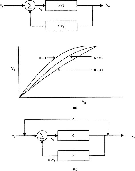
For example, in many applications, bias current can cause offset errors and errors in the transfer function of the circuit. For example, Figure 2-11(a) shows a photodiode amplifier application. Photodiodes generate a current output proportional to the light intensity falling on the photodiode. These currents, however, usually are in the subnanoamp range. The circuit of Figure 2-11(a) is simply a current-to-voltage converter. An ideal op amp would cause all the current from the photodiode to flow through the feedback resistor, causing the output voltage of the circuit to be linearly proportional to the current from the photodiode. A real op amp would lose some of the photodiode current into its input terminal. If the photodiode current is 10 nA, then an op amp with a 1 nA bias current would cause only 9 nA of signal to pass, causing a 10% error. If the amplifier has a 75 fA bias current, then the error caused by the amplifier is only 0.00075%.

In a pH transducer application such as Figure 2-11(b), a low bias current amplifier is used for two reasons: The OPA111 is an FET input device, thereby giving it an extremely high input impedance. Since the pH probe is a high-impedance element, the input impedance must be even higher. Low bias current also is necessary, since with a source impedance of 500 MΩ, a 1 nA bias current would cause an offset error of 500 mV. The signal output of the probe is only 50 mV; offset error is ten times the signal.
In critical applications where noise can contribute significant errors, such as data acquisition system front ends or audio applications, op amps with a low voltage noise density are crucial. Figure 2-11(c) shows an audio application. Preamplifiers for audio deal with small signal levels; noise that is negligible in large signal applications suddenly becomes a concern when the signal is only an order of magnitude above the noise (an S/N ratio of 20 dB).
2.4.1.1 Closed-Loop Gain and Bandwidth of VOA
Equivalent open-loop voltage gain-related components of VOAs are shown in Figure 2-12(a). With A = gmZz, where gm is the transconductance of the input stage and Zz is the parallel impedance formed by Rz and Cz. The transfer function of the closed-loop gain of the amplifier, configured for the noninverting case (Figure 2-12(b)) is given by
VoutVin=G(AA+G+R2ri)

where
G=1+R2R1

A=open‐loopgain=gmZz;ri=differentialinputimpedance.
For a VOA, ri → ∞ and the equation (2.11) can be simplified to
VoutVin=G(A)(A+G)

It is important to stress at this stage that, since the VOA is a high differential input impedance device, when negative feedback is applied in this way, voltage is sampled at the output and fed back as a voltage signal to the input. The VOA generally is internally compensated to give a low-frequency dominant pole, f0, and so the open-loop gain is A = A0[1 + j (f / f0)], where f0 ≈ 1/(2πRzCz) and A0 is the low-frequency open-loop voltage gain. Substituting this into equation (2.14) gives
VoutVin=GA0(A0+G)(11+jfGfT)

But A0/(A0 + G) ≈ 1, since A0 >> G, and therefore
VoutVin=G(11+jfGfT)
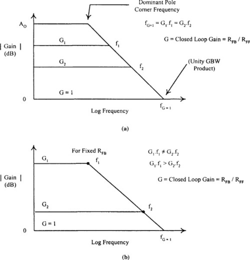
where (A0 + G) f0 ≈ A0f0 = f T, since A0 >> G, and this is the gain-bandwidth product of the VOA, which is constant. The closed-loop bandwidth (f p) of the amplifier is f p = f T /G; therefore increasing G results in a decrease in the closed-loop bandwidth, while a decrease in G leads to an increase in f p. This is the “classical” gain-bandwidth trade-off exhibited by a voltage amplifier with a single dominant-pole frequency response. The maximum closed-loop bandwidth of f T will be obtained when 100% feedback is applied; that is, when G = 1. Generally, VOAs are internally compensated for resistive feedback to guarantee stable operation for any value of G, including G = 1.
The equivalent circuit for a voltage feedback op amp is shown in Figure 2-13(a). Figure 2-13(b) shows the classic gain versus frequencyfd response obtained with dominant pole compensation. The 6 dB/octave roll-off is the optimum choice for best phase margin and fastest settling time. The product of the closed-loop gain and the closed-loop bandwidth (gain-bandwidth product) is constant for fixed compensation. The closed-loop bandwidth therefore varies inversely with the closed-loop gain.
2.4.1.2 High-Speed Voltage Feedback Op Amps
Within the last decade, many op amps with high-speed capability have entered the market to supply the demand for high-speed A/D converters, video signal processing, and other industrial needs. Many of these op amps combine high speed and precision. For example, the devices introduced by Analog Devices in the late 1980s, such as the AD840, 841, and 842 devices, are designed to be stable at gains of 10, 1, and 2 with typical gain-bandwidths of 400, 40, and 80 MHz, respectively.
A simplified schematic of high-speed voltage feedback is shown in Figure 2-14. For purposes of discussion, the amplifier is shown in the inverting mode. The amplifier consists of a differential input stage (common emitter), a voltage amplification stage, and a class AB (push-pull) output driver.

An example of such a device is the AD847 from Analog Devices. The AD847 is fabricated on Analog Devices’ proprietary complementary bipolar (CB) process, which enables the construction of PNP and NPN transistors with similar values of f T in the 600–800 MHz region. The AD847 circuit (Figure 2-15) includes an NPN input stage followed by fast PNPs in the folded cascade intermediate gain stage. The CB PNPs also are used in the current-amplifying output stage. The internal compensation capacitance that makes the AD847 unity gain stable is provided by the junction capacitance of transistors in the gain stage.
The capacitor, CF, in the output stage mitigates against the effect of capacitive loads. At low frequencies and with low capacitive loads, the gain from the compensation node to the output is very close to unity. In this case, CF is boot-strapped and does not contribute to the compensation capacitance of the part. As the capacitive load is increased, a pole is formed with the output impedance of the output stage. This reduces the gain, and therefore, CF is completely boot-strapped. Some fraction of CF contributes to the compensation capacitance, and the unity gain bandwidth falls. As the load capacitance is increased, the bandwidth continues to fall and the amplifier remains stable. For more details related to high-speed VOAs, see Analog Devices (1990).
2.4.1.3 Grounding and Bypassing
In designing practical circuits with devices such as AD847, remember that, whenever high frequencies are involved, some special precautions are in order. Circuits must be built with short interconnection leads. A large ground plane should be used whenever possible to provide a low-resistance, low-inductance circuit path as well as minimizing the effects of high-frequency coupling. Sockets should be avoided because the increased interlead capacitance can degrade bandwidth.
Feedback resistors should be of low enough value to assure that the time constant formed with the capacitance at the amplifier summing junction will not limit the amplifier performance. Resistor values of less than 5 kΩ are recommended. If a larger resistor must be used, a small (< 10 pF) feedback capacitor in parallel with the feedback resistor, RF, may be used to compensate for the input capacitance and optimize the dynamic performance of the amplifier. Power supply leads should be bypassed to ground as close as possible to the amplifier pins. Ceramic disc capacitors of 0.1 μF are recommended.
2.4.2 Current Feedback Op Amps
The current feedback operational amplifier (CFOA) is a relatively new arrival to the analog designer’s tool kit. The first monolithic device was produced by Elantec Inc. in 1987.
Current feedback operational amplifiers were introduced primarily to overcome the bandwidth variation, inversely proportional to closed-loop gain, exhibited by voltage feedback amplifiers. In practice, current feedback op amps have a relatively constant closed-loop bandwidth at low gains and behave like voltage feedback amplifiers at high gains, when a constant gain bandwidth product eventually results. Another feature of the current feedback amplifier is the theoretical elimination of slew-rate limiting. In practice, component limitations do result in a maximum slew rate, but this usually is much higher (for a given bandwidth) than with voltage feedback amplifiers.
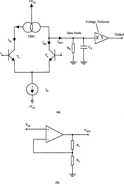
The current feedback concept is illustrated in Figure 2-16. The input stage now is a unity-gain buffer, forcing the inverting input to follow the noninverting inputl Thus, unlike a conventional op amp, the latter input is at an inherently low (ideally zero) impedance. Feedback always is treated as a current and, because of the low impedance inverting terminal output, R2 always is present, even at unity gain. Voltage imbalances at the inputs cause current to flow into or out of the inverting input buffer. These currents are sensed internally and transformed into an output voltage. The transfer function of this transimpedance amplifier is A(s); the units are in ohms.
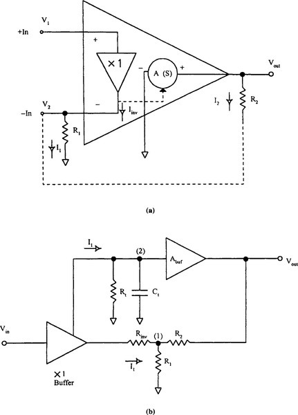
It can be shown that, if A(s) is high enough (like the open-loop gain of a conventional op amp), very little current flows in the inverting input at balance. The overall closed-loop transfer function becomes
VoutVin=(1+R2R1)

which is the same as a conventional op amp.
However, if the dominant pole is created by feeding the current imbalances into the compensation capacitor, the time constant will be set by the product of this capacitor (Ct) and the feedback resistor R2. The closed-loop bandwidth now is given by
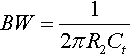
BW=12πR2Ct
and is independent of closed-loop gain. A more complete mathematical analysis can be obtained using the representative model shown in Figure 2-16(b). Notice that the input buffer has been given a finite output impedance (Rinv) to model practically realizable buffers. The error current from the buffer is mirrored and fed into a transimpedance stage consisting of Rt and Ct, where the current-to-voltage conversion takes place. The voltage generated here is buffered by another unity-gain stage and fed to the main amplifier output. Because the value of the small-signal transresistance, Rt, is very high (often in the megaohm range), only minute error currents are needed to change the voltage at node 2 by several volts. Consequently, the amount of current that must flow into or out of the inverting input terminal under steady-state conditions is extremely small. The feedback network, even though it may be formed from quite low-value resistors, therefore presents a very light effective load on the output of the input buffer.
Applying Kirchhoff’s law to nodes of circuit in Figure 2-16(b), the overall transfer function and the like can be derived (Toumazou, Lidgey, and Haigh, 1990, Chapter 16). It can be shown that, if the product of Rt and Abuf is large, the closed-loop gain approaches [1 + (R2/R1)] as the transconductance approaches infinity, which is the same result as a VOA with large open-loop gain. The AC behavior would appear to be somewhat less intuitive; however, if the product of Rt and Abuf is large enough, the closed-loop pole frequency can be closely approximated by
fpole=Abuf2π[R2+(1+R2R1)Rinv]Ct
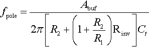
This result indeed is very different from the constant gain-bandwidth product of a voltage feedback amplifier. At low gains, when R2 >> Rl, and assuming Rbuf << R2 (which always is true in practice), the closed-loop pole frequency is dictated predominantly by the compensation capacitor and the feedback resistor, R2, and is substantially independent of the exact gain setting. Therefore, the choice of feedback resistor is of somewhat more importance than in the case of voltage feedback amplifiers, and most manufacturers will state a suggested minimum to avoid oscillation problems.
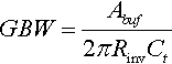
At high gains (in practice 50 or more could be considered high), the Rinv term becomes dominant and the amplifier asymptotically assumes a constant gain-bandwidth product given by
GBW=Abuf2πRinvCt
The gain of the output buffer, Abuf, also plays its part in determining the closed-loop pole frequency. As the main amplifier output is loaded, the gain drops below unity and causes a reduction in closed-loop bandwidth predicted by equation (2.19). This also tends to make practical amplifiers more stable when heavily loaded. With a constant load, the bandwidth reduction can be compensated for by reducing the value of the feedback resistor.
This theory, although useful, in practice (as always) is compounded by second-order poles and zeroes and stray capacitive and parasitic inductive effects. Such limitations manifest themselves principally as peaking in the small signal response, overshooting and ringing in the transient response, and a sensitivity of overall AC behavior to loading conditions.
The most significant advantages of the CFOAs are
• The slew-rate performance is high, where typical values could be in the range of 500-2500 V/μS (compared to 1−100 V/μs for VOAs).
• The input referred noise of CFOA has a comparatively lower figure.
• The bandwidth is less dependent on the closed-loop gain than with VOAs, where the gain-bandwidth is relatively constant.
2.4.2.1 Practical High-Speed Current Feedback Amplifiers
The equivalent circuit for a current feedback op amp is shown in Figure 2-17. An ideal current feedback amplifier has no input impedance at its inverting input (Rin = 0), infinite input impedance at its noninverting input, and the voltage at the inverting input is held at that of the noninverting input by a unity gain buffer. The transfer function of this amplifier (Vout/Iin) is a dimensional quantity with the dimension of a resistance, not a ratio, as in the case of voltage feedback op amps. Because of the very low (ideally zero) inverting input impedance, the current feedback op amp has a bandwidth more or less independent of closed-loop gain for a fixed feedback resistor RFB. This implies that the product of the closed-loop gain and the closed-loop bandwidth is not a constant; hence, it is inappropriate to apply the term gain-bandwidth product to current feedback amplifiers. Examples of practical devices are AD844 and AD846 from Analog Devices and HA5004 from Harris Semiconductors. Figure 2-18 compares the frequency response of CFOA with VOA.
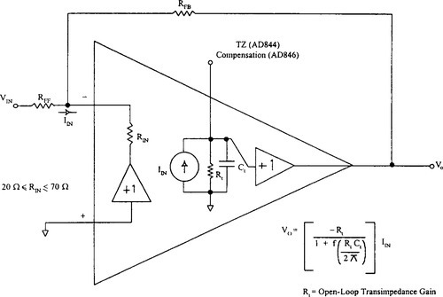
The practical current feedback amplifier is based on a common base input stage, as shown in Figure 2-19. This configuration is characterized by a high impedance noninverting input, which drives the inverting input via a unity gain buffer. The open-loop inverting input impedance is approximately equal to any resistance in series with the emitter (RE) plus the dynamic input impedance of the grounded base transistor (rE). The output voltage is controlled by the input current and is related to it by the transimpedance gain expressed in ohms. Because of the low-impedance inverting input common base stage, a stepped input voltage ∆Vin will produce a stepped current in the emitter and collector of Q1. This will yield a slew rate of Iin/Cc. Therefore, the rise and fall times of the output essentially are constant regardless of the output voltage swing. This attribute provides for exceptional full-power bandwidth. Bandwidth characteristics for several current feedback op amps are shown in Table 2-2. For further details on applications and design techniques on CFOAs, see Analog Devices (1990), Lidgey and Hayateleh (1997), Toumazou et al. (1990, Chapter 16), and Mancini and Lies (1995).
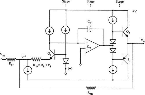
Table 2-2
Bandwidth Comparison of Few CFOA.
| Device | RFB | RFF | Gain | Closed-Loop Bandwidth (CLBW) | Gain-Bandwidth Product (GBW) |
| AD846 | 1000 Ω | 1000 Ω | − 1 | 46 MHz | 46 MHz |
| 1000 Ω | 100 Ω | − 10 | 20 MHz | 200 MHz | |
| AD844 | 500 Ω | 500 Ω | − 1 | 60 MHz | 60 MHz |
| 500 Ω | 50 Ω | − 10 | 33 MHz | 330 MHz | |
| AD9617 | 400 Ω | 400 Ω | ± 1 | 185 MHz | 185 MHz |
| 400 Ω | 27 Ω | ± 15 | 105 MHz | 1575 MHz | |
| AD9611 | 1000 Ω | 1000 Ω | − 1 | 300 MHz | 300 MHz |
| 1000 Ω | 50 Ω | − 20 | 200 MHz | 4000 MHz |

(Reproduced by permission of Analog Devices, Inc.)
2.4.3 Single-Rail Op Amps
Single-supply operation is becoming an increasingly important requirement as systems get smaller, cheaper, and more portable. Portable systems rely on a battery as the primary power source. Consequently, power consumption and operating time per battery charge are high on the designers’ priority list. This makes low-voltage operation and low power consumption critical.
Most general purpose op amps are designed to operate from ± 15 V supplies. Trying to make them work at low voltages may require special attention because few are specified to operate at lower voltages. Many even will not function at 5 V or less. In modern products designed to operate from batteries (such as two 1.5 V cells), designers must consider some aspects that are less serious in high rail voltage-based systems. Some important ones follow:
1. A low signal swing compresses signal-to-noise performance.
2. The noise floor tends to rise at low currents.
3. Choosing the ground reference becomes important.
4. The bandwidth suffers as the supply current drops.
2.4.3.1 Effect of Reduced Signal-to-Noise Performance
The most immediate effect on an amplifier circuit running on single supply at a reduced voltage is the reduction in signal swing. Even if the noise floor remains constant (highly unlikely), the signal-to-noise performance will drop as the signal amplitude decreases.
Most op amps that are designed to operate from ± 15 V usually have no problem with output headroom: 3−4 V is sufficient for most applications. However, if the supply voltages drop to, say + 12 V, a 3 V headroom requirement (at each rail) would limit the signal swing to 6 V P-P (from + 3 V to + 9 V). Dropping the voltage further to + 5 V will render these op amps inoperable, as no output swing capability is left.
For this reason and others, low-voltage single-supply op amps are designed so that their output stage swings as closely to both rails as possible. This helps to restore some of the lost signal-to-noise performance. It is useful if the output can swing to the negative rail. Many op amps have this capability. Single-rail op amps are designed to require 1 or 2 V at most as headroom. Some special designs could have even less headroom, allowing them to operate at + 5 V or less. The drawback is that most of these op amps are not designed to source much output current, usually 5 mA or less.
In addition to being compressed at the high-level end by signal reduction, the signal-to-noise performance generally is squeezed from the bottom end as well, as noise floor tends to rise. This is because the single supply usually accompanies an inevitable drive toward lower supply current consumption, which tends to increase noise. The designer must decide how these issues affect the final performance target of the system and make the necessary trade-offs.
2.4.3.2 Ground Reference
Most dual-rail op amps use the signals referenced to 0 V, which is the midpoint of ± Vcc rail. This is the most convenient, as there is ample supply headroom to work with. Such is not the case for single-supply circuits. Ground reference can be chosen anywhere within the supply range of the circuit. There is no standard to follow. Indeed, the choice of ground reference depends on the types of signals used. To illustrate this point, choosing the negative rail as the ground reference may optimize the signal dynamic range of an op amp designed to swing to 0 V. On the other hand, the signal may have to be level shifted to be compatible with another device that is not designed to operate at 0 V input because the signal no longer can be inverted. These limitations can force an inefficient design, increasing the cost of the system.
Choosing the negative rail as the ground reference is the simplest and most natural choice for setting the ground reference. Since the negative rail is the return of the supply, its impedance is very low and it makes an ideal ground reference. All signals can be returned to this point without concern about its ability to sink the current, assuming the current is within the rated capability of the supply. Nevertheless, the voltage drop in negative rail ground returns can be a problem, and their resistance must be kept low.
Setting the ground reference at the negative rail usually allows the maximum signal dynamic range, as it establishes the limit of one end of the signal range. However, this may present a problem interacting with other devices, as their inputs or outputs are not designed to operate near the negative rail. Therefore, it is important to know what types of devices are needed for the application, knowing that the signal will’ swing to the negative rail.
Not all single-supply circuits work well with the 0 V ground system. For example, audio or video signals may be best handled using a false-ground system by biasing the amplifiers to the midpoint of the supply. Then the signal can be AC coupled through the amplifier chain. This removes the necessity of level shifting at each amplifier stage, as otherwise would be required if the 0 V ground system is used. It also saves the cost of additional components to do the level shifting.
It often is assumed that a false-ground circuit need be only a simple buffer amplifier without the bypass capacitors and compensation. In some cases, one can get by without them as long as the false-ground node sees no dynamic or transient load changes. These can occur when driving the ground pin of a D/A or an A/D converter. In these applications, the false-ground node must hold its voltage constant with minimum perturbation. In the presence of reference “bounce,” conversion error may result or noise may be injected into the circuit.
The choice of the quality of the false-ground rests on whether the circuit is sensitive to false-ground perturbation, both in DC and AC terms. Not all applications necessarily require a high-quality, low-impedance false-ground. In fact, in some cases, it may be sensible to use both false-ground and negative-rail ground references in different parts of the circuit. One needs to observe the level shifting requirement at interfaces of the two; it depends on what works best.
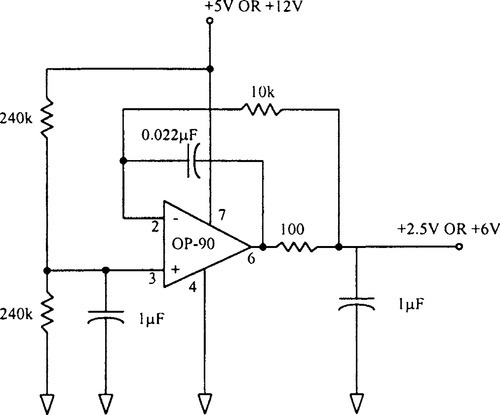
A solid false-ground can be implemented easily using a voltage divider or reference voltage buffered by an amplifier. The choice of the op amp and the implementation are critical to a good reference node with no reference “bounce.” An example is shown in Figure 2-20, and further details may be found in Analog Devices (1992).
2.4.3.3 Handling O V Input Signals
Dual-rail op amps, which generally are designed with NPN input transistor pairs, usually cannot handle signals that are at or near the negative rail, due to the requirement of 2–3 V headroom at either rail. Operating at or near the negative rail would cause the amplifier to go nonlinear as saturation is approached. Even worse, it may cause the output to reverse its phase.
Op amps designed for single-supply operation typically use PNP input pairs to allow the input to operate linearly at or near the negative rail. Another input architecture that can operate at 0 V uses MOSFET transistors in a CMOS amplifier. An example is OP-80 from Analog Devices, which has a P-channel input pair.
2.4.3.4 Handling O V Output Signals
Ideally, a single-supply op amp’s output should be capable of swinging to the negative rail, especially if it is feeding into the input of the next stage that can operate at 0 V. Beware that, as the output swings very near the negative rail, the output accuracy can drop off rapidly, as a function of the (output sink) load current. This is because a single-supply amplifier’s output stage usually has either an active transistor pull-down or it may require a resistor to pull-down to the negative rail. Whatever the means, the pull-down’s finite resistance develops a voltage drop that prevents the output from swinging fully to the negative rail. If accuracy is required at or near 0 V, the load current must be kept as small as practical. Always keep in mind that the total load current also includes the current flow in the feedback resistor. As mentioned previously, some op amps have an active output drive to the negative rail. Others require a resistor pull-down to achieve a complete swing to 0 V. Figure 2-21 shows both topologies.
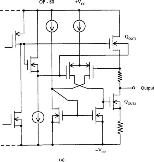
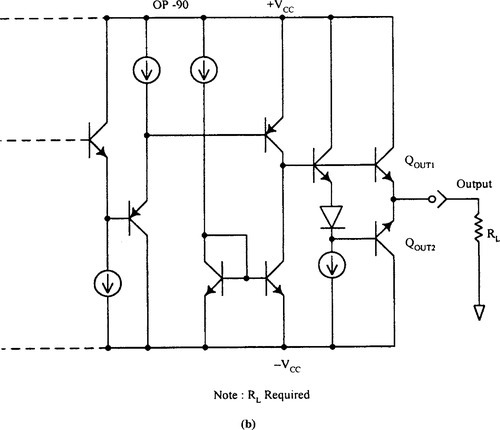
Figure 2-21(a)’s OP-80 output stage relies on the internal on-resistance of QOUT2 to pull the output down to the negative rail. Including a source resistance, the total pull-down resistance typically is 400 Ω. As long as the load current is less than 1 μA, its output will swing to within 1 mV of the negative rail.
The OP-90 utilizes a conventional push-pull emitter-follower output stage, as shown in Figure 2-21(b). This provides a low-impedance drive except for output voltages less than 0.5 V to the negative rail. Below this voltage, the bottom output transistor QOUT2 saturates, clamping the output at a base-emitter voltage above the negative rail. If no external pull-down resistor is provided, the top output transistor QOUT1 turns off completely, as its base voltage tends to pull less than its base-emitter voltage, cutting off the base drive. However, a pull-down resistor would keep the QOUT1 active, and therefore linear operation would continue as the output swings to the negative rail. For applications and other design data about these examples, see the device data sheets.
Op amps whose output is designed to swing from one rail to the other are ideally suited for single, reduced supply operation. Theoretically, the maximum signal-to-noise performance for a given supply voltage can be achieved. One such rail-to-rail device is the OP-295 dual operational amplifier (Analog Devices, 1992).
Most industry standard precision op amps are designed to operate with dual, higher voltage (± 15 V) supplies. Their precision performance is optimized for these supply voltages. As such, trying to operate them at lower voltages may be inadvisable, as their specifications may no longer apply. Indeed, many do not function even if their input is forced to the negative rail or if they are powered by a single + 5 V supply.
Very few single-supply op amps exhibit sufficiently low input offset and offset drift to qualify them as precision op amps. The OP-90, OP-290, and OP490 come close to precision performance yet can operate off a single supply.
For a comprehensive practical discussion on single-supply operation, devices, applications, and restrictions, see Analog Devices (1992).
2.4.4 Micro-Power Op Amps
Numerous op amps on the market perform well at supply currents in the 500 μA−1 mA range, but certain applications require devices that operate at even lower currents. For example, applications that rely on batteries or solar cells need to keep current drain to a minimum. Low-current operation also is essential for minimizing power dissipation in equipment containing large quantities of tightly packed active components.
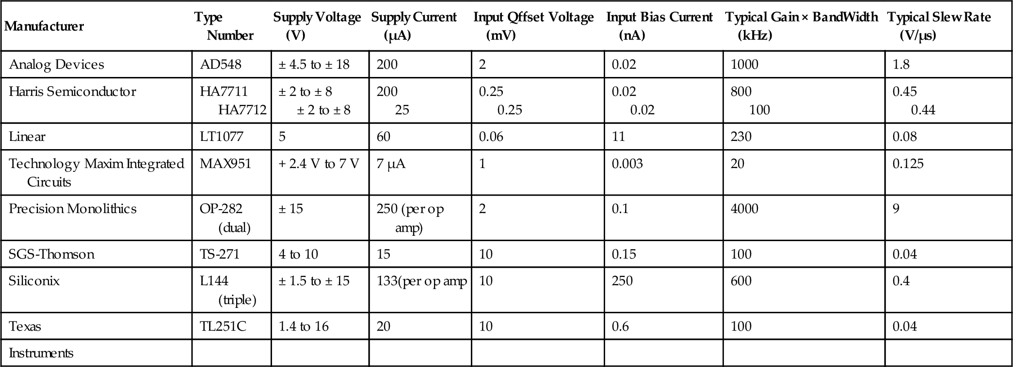
Micro-power op amps can meet these needs. Although definitions of the term vary, all micro-power devices perform at currents lower than the 500 μA minimum of “low-power” devices. Op amps that operate below about 250 μA supply currents generally can be categorized as micro-power devices. Table 2-3 indicates a representative group of micro-power op amps and their characteristics.
Table 2-3
Representative Micro-Power Op Amps
| Manufacturer | Type Number | Supply Voltage (V) | Supply Current (μA) | Input Qffset Voltage (mV) | Input Bias Current (nA) | Typical Gain × BandWidth (kHz) | Typical Slew Rate (V/μs) |
| Analog Devices | AD548 | ± 4.5 to ± 18 | 200 | 2 | 0.02 | 1000 | 1.8 |
| Harris Semiconductor | HA7711 HA7712 | ± 2 to ± 8 ± 2 to ± 8 | 200 25 | 0.25 0.25 | 0.02 0.02 | 800 100 | 0.45 0.44 |
| Linear | LT1077 | 5 | 60 | 0.06 | 11 | 230 | 0.08 |
| Technology Maxim Integrated Circuits | MAX951 | + 2.4 V to 7 V | 7 μA | 1 | 0.003 | 20 | 0.125 |
| Precision Monolithics | OP-282 (dual) | ± 15 | 250 (per op amp) | 2 | 0.1 | 4000 | 9 |
| SGS-Thomson | TS-271 | 4 to 10 | 15 | 10 | 0.15 | 100 | 0.04 |
| Siliconix | L144 (triple) | ± 1.5 to ± 15 | 133(per op amp | 10 | 250 | 600 | 0.4 |
| Texas | TL251C | 1.4 to 16 | 20 | 10 | 0.6 | 100 | 0.04 |
| Instruments |
2.4.5 Chopper-Stabilized Op Amps
The best bipolar op amps may have offsets as low as 10 μV. When a design requires an extremely low input offset voltage (Vos) with virtually no offset-voltage drift over time or temperature, chopper-stabilized devices are available from many manufacturers.
Low offset-voltage drift probably is the most attractive characteristic of chopper-stabilized op amps. Applications that take advantage of this feature include strain-gauge amplifiers, thermocouple amplifiers, and precision data collection in environments where periodic adjustments are either impractical or impossible. Most often these applications involve low-frequency signals (less than 10 Hz).
Figure 2-22 shows the basic operation of a chopper-stabilized op amp. The device consists of a clock generator, a main and a nulling amplifier, and two holding capacitors, which can be either internal or external. The main amplifier has fixed connections to the input and output pins.

The nulling amplifier alternately performs two tasks. First, it uses a holding capacitor (C1) to store a correction for its own offset, which is measured while the amp’s input pins are shorted. The hulling amp then measures the offset of the main amplifier and stores a correction voltage in another capacitor (C2). The amplifier alternates between these tasks at the rate of the clock. Because the op amp is constantly correcting its offset, offset voltages are low and drift is virtually nonexistent.
Practical examples of such op amps are ICL7650S from Intersil or Harris Semiconductor and MAX430 from Maxim Integrated Circuits. Typical specifications of the ICL76505 type devices are 5 μV of Vos and an input bias current of 10 pA at 25°C. Offset drift averages 0.02 μV/°C within the range of − 25 to 80°C.
The ICL76505 requires external holding capacitors to operate, but devices such as MAX430 have 0.1 μF chip capacitors bonded to the lead frame within the device. Such devices that operate from ± 15 V power supplies allow you to directly replace conventional LM741 or LM 108 devices.
Early chopper-stabilized amplifiers actually used relays to chop the signal, but today such amplifiers are monolithic and use MOS switches to do the job. Early monolithic amplifiers of this type had high noise at the chopping frequency (which may be between a few hundred Hz and a few tens of kHz). This high-frequency noise is less of a problem in the latest devices, which may contain quite effective filters at the chopper frequency (although careful layout and supply decoupling still are important with these parts), but switching noise remains the major problem with chopper-stabilized op amps. Because of the technology used to manufacture them (frequently CMOS), many chopper-stabilized op amps have a voltage noise of several μV in the band 0.1−10 Hz, and it therefore is necessary to integrate their output for several seconds or tens of seconds to obtain the low offset of which they are potentially capable. Not all systems allow such long integration times, and so a compromise becomes necessary between offset and speed. Table 2-4 compares the precision op amps versus chopper stabilized amplifiers.
Table 2-4
Comparison of Precision Op Amps vs. Choppers.
| Parameter | Precision (Bipolar) Op Amps | Chopper |
| Offset voltage | 10–50 μV | < 5 μV |
| Offset drift | 0.1 μV/°C | ~ 0 μV |
| Open-loop gain | 107 | 107 |
| Noise: HF glitch | None | > 100 mV P-P |
| Noise: 0.1−l0 Hz | < 0.2 μV P-P | > l μV P-P |
| Cost | Lower | Higher |
| External components | None | Some require 2 capacitors |
| Saturation recovery | 10–20 μs | > 100 ms to seconds |
(Reproduced by permission of Analog Devices Inc.)
For amplifiers that have no built-in capacitors, such as the Intersil 7650S and the 420 series from Intersil and Maxim, you must select the hold capacitors carefully. Noise really is not the critical issue; any low-leakage capacitor is adequate in this regard. But settling time is an issue; capacitors with a high dielectric absorption, such as ceramic capacitors, can take several seconds to settle after power first is applied. Therefore, you should use Mylar or polypropylene capacitors if you need fast initial settling.
When a chopper-stabilized amplifier is overloaded due to saturation, capacitors can acquire excessive charges and it could take a long time to recover when the overload is removed. To avoid the recovery time problem, many chopper-stabilized op amps use clamp circuits that prevent the amplifier from reaching saturation during an overload. Figure 2-23 shows a circuit that prevents the op amps from reaching saturation. When VOUT approaches either rail, the appropriate clamp transistor begins conducting. Connecting the clamp pin to the amplifier’s inverting input pin puts that transistor in parallel with the gain resistor. As the transistor conducts, it reduces the gain of the amplifier, thus preventing saturation.
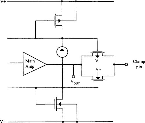
But using the clamp has two drawbacks. First, the available output range of the amplifier is reduced by as much as 1 V from each rail. Second, the leakage of the clamp transistors shows up as additional bias current at the input and reduces accuracy. Typical leakage currents range from 1 to 10 pA.
The sampling techniques that chopper-stabilized op amps use to eliminate drift can result in intermodulation as well as clock noise. Interaction between the input signals and the clock can generate intermodulation products in the form of sum and difference signals. If the input signal’s frequency is close to the rate of the clock, the difference product shows up as additional offset error. You can eliminate this error by filtering the input signal to keep its frequency range well below the sampling clock frequency. To avoid intermodulation problems, many chopper amps allow the designer, using an external signal, to set the clock frequency of the amplifier. For further details, see Quinnell (1989) and Harris Semiconductor (1993–94).
2.4.6 High-Voltage Power Op Amps
For power amplifier applications, special components are available from a limited number of manufacturers. Today, high-voltage amplifiers with total (rail-to-rail) voltages of 1200 are capable of driving around 75 mA to a load. The PA89 hybrid IC from Apex Microtechnology Corporation is an example. Similarly, high-current amplifiers, which can handle as high as 30 A, with 150 V rail to rail, are available from the some manufacturers. The PA03 power operational amplifier from Apex is an example. Some applications of such special power op amps are sonar transducer drivers, piezoelectric transducer drivers, high-voltage instrumentation, programmable power supplies, and linear and rotary motor drivers. Figure 2-24 shows some of these hybrid devices.

In these types of op amps, the designer has to consider many special situations, such as power supply performance, thermal management, safe operating area, and stability. A discussion of these topics is beyond the limits of this chapter. Application notes in Apex Microtechnology Corp. (1996, pp. D1−D105) provide an excellent discussion.