
Digital Signal Processors
5.1 Introduction
The processing of information is as old as the human race. The technology associated with it dates back to before the earliest form of writing to the use of counting beads and to the time of cave drawings. However, the inventions of printing (1049), the electronic binary coding of data (1837), and more recently radio communications (1891) and the electronic digital computer (1946) have increased the speed of generation and processing of data to such an extent that information and control technology no longer is concerned just with automatic processes replacing manual ones but provides the opportunity to do entirely new things. The developments during the 50 or so years since the invention of the transistor (1948) have helped designers introduce products that can hear, talk, and even detect the motion of objects. The late 1990s have seen developments related to automatic processes that could replace human sensory and cognitive processes as well as manipulative ones.
Early generations of 4- and 8-bit CISC processors have evolved into 16-, 32-, and 64-bit components with CISC or RISC architectures. Digital signal processors can be considered special cases of RISC architecture or sometimes parallel developments of CISC systems to tackle real-time signal processing needs. Over the past several decades, the field of digital signal processing has grown from a theoretical infancy to a powerful practical tool and matured into an economical yet successful technology.
At its early stages, audio and the many other familiar signals in the same frequency band have appeared as a magnet for DSP development. The 1970s saw the implementation of special signal processing algorithms for filters and fast Fourier transforms by means of digital hardware developed for the purpose. Early sequential program DSPs are described by Jones and Watson (1990).
In the late 1990s, the market for DSPs is generated mostly by wireless, multimedia, and similar applications. As per industry estimates, by the year 2001, the market for DSPs is expected to grow to about $9.1 billion (Schneiderman, 1996). Currently, communications represent more than half of the applications for DSPs (Schneiderman, 1996). This chapter provides an essential guide for designers to understand the DSPs and briefly compares microprocessors and DSPs.
5.2 What Is a DSP?
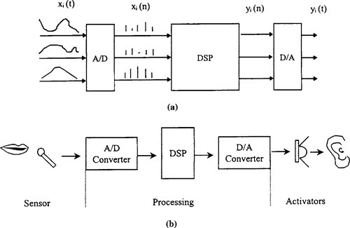
A digital signal processor accepts one or more discrete-time inputs, xi(n), and produces one or more items of output, y1(n), for n = …, −1,0, 1,2,…, and I = 1, …, N, as depicted in Figure 5-1(a). The input could represent appropriately sampled (and analog-to-digital converted) values of continuous time signals of interest, which are processed in the discrete-time domain to produce output in discrete time that could then be converted to continuous time, if necessary. The operation of the digital signal processor on the input samples could be linear or nonlinear, time invariant or time varying, depending on the application of interest. The samples of the signal are quantized to a finite number of bits, and this word length can be either fixed or variable within the processor. Signal processors operate on millions of samples per second, require large memory bandwidth, and are computationally very demanding, often requiring as many as a few hundred operations on each sample processed. These real-time capabilities are beyond the capabilities of conventional microprocessors and mainframe computers. A practical example of voice processing by a DSP is shown in Figure 5-1(b).
Signal processors can be either programmable or of a dedicated nature. Programmable signal processors allow flexibility of implementation of a variety of algorithms that can use the same computational kernel, while dedicated signal processors are hardwired to a specific algorithm or class of algorithms. Dedicated processors often are faster than or dissipate less power than general purpose programmable processors, although this is not always the case.
Digital signal processors traditionally have been optimized to compute the finite impulse response convolutions (sum of products), infinite impulse response recursive filtering, and fast Fourier transform-type (butterfly) operations that typically characterize most signal processing algorithms. They also include interfaces to external data ports for real-time operation. It is interesting to note that one of the earliest digital computers, ENIAC, included characteristics of a DSP (Marven and Ewers, 1994).
5.3 Comparison Between a Microprocessor and a DSP
Following the preceding chapter’s discussion of microprocessors and microcontrollers, we can compare the microprocessors and DSPs. General architectures for computers and single-chip microcomputers fall into two categories. The architectures for the first significant electromechanical computer had separate memory spaces for the program and the data, so that both could be accessed simultaneously. This is known as a Harvard architecture, having been developed in the late 1930s by Howard Aiken, a physicist at Harvard University. The Harvard Mark 1 computer became operational in 1944.
The first general purpose electronic computer was probably the ENIAC (electronic numerical integrator and calculator) built during 1943–1946 at the University of Pennsylvania. The architecture was similar to that of the Harvard Mark 1 with separate program and data memories. Due to the complexity of two separate memory systems, Harvard architecture has not proven popular in general purpose computer and microcomputer design.
A consultant to the ENIAC project, John von Neumann, a Hungarian-born mathematician, is widely recognized as the creator of a different, very significant architecture, published by Burks, Goldstine, and von Neumann (1946; reprinted in Bell and Newell, 1971). The so-called von Neumann architecture set the standard for developments in computer systems over the next 40 years and more. The idea was very simple, based on two main premises: that there is no intrinsic difference between instructions and data and that instructions can be partitioned into two major fields containing the operation command and the address of the operand (data to be operated on); therefore, a single memory space could contain both instructions and data.
Common general purpose microprocessors, such as the Motorola 68000 family and the Intel i86 family, share the von Neumann architecture. These and other general purpose microprocessors also have other characteristics typical of most computers over the past 40 years. The basic computational blocks are an arithmetic logic unit and a shifter. Operations such as add, move, and subtract are performed easily in a very few clock cycles. Complex instructions such as multiply and divide are built up from a series of simple shift, add, and subtract operations. Devices of this type are known as complex instruction set computers. CISC devices have multiply instructions, but this will simply execute a series of microcode instructions which are hard coded in on-chip ROM. The microcoded multiply operation therefore takes many clock cycles.
Figure 5-2 compares the basic differences between traditional microprocessor architecture and typical DSP architecture. Real-time digital signal processing applications require many calculations of the form

This simple equation involves a multiplication operation and an addition operation. Because of its slow multiplication, a CISC microcomputer is not very efficient at calculating it. We need a machine that can multiply and add in just one clock cycle. For this, we need a different approach to computer architecture.
Many embedded applications are well defined in scope and require only a few calculations to be performed, but they require very fast processing. Examples of such applications are digital compression of images, compact disc players, and digital telephones. In addition to these computation-intensive functions demanding the continuous processing, the processor has to perform comparatively simple functions such as menu control for satellite TV, selection of tracks for CD players, or number processing in a digital PBX, all of which require significantly less processing power.
In such applications, computation-intensive functions such as digital filtering and data compression require continuous signal processing, which requires multiplication, addition, subtraction, and other mathematical functions. While RISC processor architectures could be optimized to handle these situations by incorporating cache memory, direct access internal registers, and the like, DSP systems provide more computation-intensive functions such as fast Fourier transforms, convolutions, and digital filters. Particularly in a DSP-based system, such tasks should be performed on a real-time basis, as per Figure 5-3. This indicates that the sample period and computational latency are becoming key parameters.
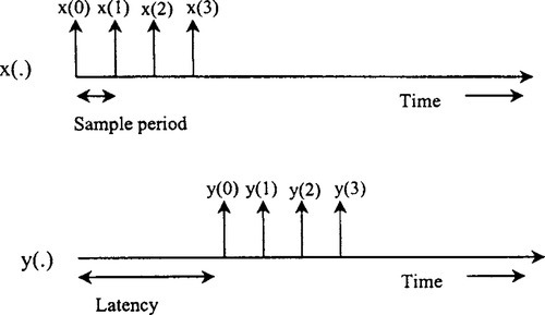
5.3.1 The Importance of the Sample Period and Latency in the DSP World
The sample period (the time interval between the arrival of successive samples of the input signal) depends on the technology employed in the processor. The time interval between the arrival of input and the departure of the corresponding output sample is the computational latency of the processor. To ensure the stability of the input ports, the output samples have to depart at the same sample period as the input samples. In signal processing applications, the minimum sample period that can be achieved often is more important than the latency of the circuit. Once the first output sample emerges, successive samples will emerge at the sample period rate, hiding the effects of a large latency of circuit operation. This makes sense because typical signal processing applications deal with a few million samples of data in every second of operation. For details on the relationship between these two parameters, see Madisetti (1995).
Other important measures are the area of the VLSI implementation and its power dissipation. These directly contribute to the cost of a DSP chip. One or more of these measures usually is optimized at the cost of others. These trade-offs again depend on the application. For instance, signal processors for portable communication require low power consumption combined with small size, usually at the cost of an increased sample period and latency.
5.3.2 The Merging of Microprocessors and DSPs
Diverse, high-volume applications such as cell phones, disk drives, antilocking brakes, modems, and fax machines require both microprocessor and DSP capability. This requirement has led many microprocessor vendors to build in DSP functionality. In some cases, such as in Siemens’ Tricore architecture (Levy, 1998a), the functional merging is so complete that it is difficult to determine whether to consider the device a DSP or a microprocessor. At the other extreme, some vendors claim that their microprocessors have high-performance DSP capability, when in fact they have added only a “simple” 16 × 16-bit multiplication instruction.
5.4 Filtering Applications and the Evolution of DSP Architecture
Digital signal processing techniques are based on mathematical concepts familiar to most engineers. From these basic ideas spring the myriad applications of DSP, including fast Fourier transform, linear prediction, nonlinear filtering, and decimation and interpolation (see Figure 5-4). One of the most common signal processing functions is linear filtering. High-pass, low-pass, and bandpass filters, which traditionally are analog designs, can be constructed with DSP techniques. To build a linear filter using digital methods, a continuous-time input signal, xc(t), is sampled to produce a sequence of numbers, x(n) = xc(nT). This sequence is transformed by a discrete-time system — that is, a computational algorithm — into an output sequence of numbers, y(n). Finally, a continuous-time output signal, yc(t), is reconstructed from the sequence y(n). The essentials of filtering and sampling as applied to the world of DSP were discussed in Chapter 3.
5.4.1 Digital Filters
Digital filters for many years have been the most common application of digital signal processors. Digital design, of any kind, ensures repeatability. Two other significant advantages accrue with respect to filters. First, it is possible to reprogram the DSP and drastically alter the filter’s gain or phase response. For example, we can reprogram a system from low pass to high pass without throwing away the existing hardware. Second, we can update the filter coefficients while the program is running; that is, build “adaptive” filters. The two basic forms of digital filter, the finite impulse response (FIR) filter and the infinite impulse response (IIR) filter, are explained next. The initial descriptions are based on a low-pass filter. It is very easy to change low-pass filters to other types: high pass, bandpass, and so forth. Parks and Burrus (1987) and Oppenheim and Schafer (1988) cover this in detail.
5.4.1.1 Finite Impulse Response Filter
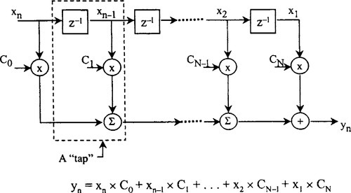
The mechanics of the basic FIR filter algorithm are straightforward. The blocks labeled z−1 in Figure 5-5 are unit delay operators; their output is a copy of the input sample delayed by one sample period. A series of storage elements (usually memory locations) are used to simulate series of these delay elements (called a delay line). The FIR filter is constructed from a series of taps. Each tap includes a multiplication operation and an accumulation operation. At any given time, n − 1 of the most recent input samples resides in the delay line, where n is the number of taps in the filter. Input samples are designated xk; the first input sample is x1, the next is x2, and so on. Each time a new input sample arrives, the previously stored samples are shifted one place to the right along the delay line and a new output sample is computed by multiplying the newly arrived sample and each of the previously stored input samples by the corresponding coefficient. In the figure, coefficients are represented as Cn, where n is the coefficient number. The results of each multiplication are summed together to form the new output sample, yn. Later we discuss how DSPs are designed to help implement these.
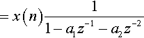
5.4.1.2 Infinite Impulse Response Filter
The other basic form of digital filter is the infinite impulse response filter. A simple form of this is shown in Figure 5-6. Using the same notations as for the FIR, we can see that
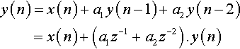
Take the math for granted — it is just relatively simple substitution. Therefore, the transfer function is given by
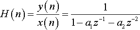
From equation (5.2) we can see that each output, y(n), is dependent on the input value, x(n), and two previous outputs, y(n − 1) and y(n − 2). Taking this one step at a time, let us assume that there were no previous input samples before n = 0, then
![]()
At the next sample instant,
Then, at n = 2,
Then, at n = 3,

We already can see that any output depends on all the previous inputs and we could go on, but the equation just gets longer. An alternative way of expressing this is to say that each output depends on an infinite number of inputs. This is why this filter type is called an infinite impulse response.
If we look again at Figure 5-6, the filter actually is a series of feedback loops, and as with any such design, we know that, under certain conditions, it may become unstable. Although instability is possible with an IIR design, it has the advantage that, for the same roll-off rate, it requires fewer taps than FIR filters. This means that, if we are limited in the processor resources available to perform a desired function, we may have to use an IIR. We just have to be careful to design a stable filter. More advanced forms of these filters are discussed with simple explanation in Marven and Ewers (1994).
5.4.2 Filter Implementation in DSPs
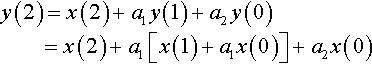
To explain the filter implementation, let us take the case of a first-order recursive filter. A signal flow graph or signal flow diagram is a convenient representation of a signal processing algorithm. Consider the first-order recursive filter shown in Figure 5-7(a). The sequential computations involved are not clearly evident in the signal flow graph, since it appears as if all the operations can be evaluated at the same time. However, operations have to follow a certain precedence to preserve correct operation. It is also not clear where the data operands and coefficients are stored prior to their utilization in the computation. A more convenient mode of description would be the one in Figure 5-7(b), which shows the storage locations for each operand and the sequence of computations in terms of micro-operations at the register-transfer level (RTL) ordered in time from left to right. We assume that the state variable v(n − 1) is stored in the data memory (DM) at location D1, while the coefficient C1 stored in a coefficient memory (CM) at location C1. Both these operands are fetched and multiplied and the result is added to the input sample, x(n), and the sum is stored in a temporary location, T1. Then, another multiplication is performed using coefficient C2 and the product is added to the contents of T1. The final result is the output y(n). The new variable v(n) is stored in memory location D1. One may wonder why temporary location T1 has been used. Temporary locations such as T1 often provide a longer word length (or precision) than the word length of the memory. Repeated sums of products, as required in this example, quickly can exceed the dynamic range provided by the word length. Temporary locations provide the additional bits required to offset the deleterious effects of overflow. One also can observe that, in this example, the multiplier and adder operate in tandem and the second coefficient multiplication can utilize the same multiplier when the input sample is being added. Thus, only one multiplier and one adder are required as arithmetic units. One data memory location, two coefficient memory locations, and one temporary storage register are required for correct operation of the filter. The specification of the sequence of micro-operations required to perform the computation is called programming in assembler.
From the preceding discussion, any candidate signal processor architecture for the IIR filter needs a coefficient memory, a data memory, temporary registers for storage, a multiplier, an adder, and interconnection. In addition, address must be calculated for the memories as well as interpretation (or decoding) of the instruction (obtained from the program memory). The coefficient memory and the program memory can be combined into one memory (the program memory). Nothing can be written into this read-only memory (ROM). Data can be written and read from the random-access data memory (RAM). The architecture shown in Figure 5-8 is a suitable candidate architecture for this application. The program counter and the index registers are used in computing the addresses of the next instruction and the coefficients. The instruction is decoded by the instruction register (IR), where the address of the data is calculated using the adder and the base index register provided with the data memory. The program bus and the data bus are separate from each other, as are the program and data memories. This separation of data and program memories and buses characterizes the Harvard architecture for digital signal processors. The shifter is provided to allow incorporation of multiple word lengths within the data path (the multiplier and the adder) and the data and program buses. The T1 register is configured as a higher-precision accumulator. Input samples are read in from the input buffer and written into the output buffer. The DSP can interact with a host computer via the external interface. In Figure 5-8, the integers represent the number of bits carried on each bus. For a detailed account of digital filters, see Jones and Watson 1990, (Chapter 7).

The inherent advantages of digital filters are these:
1. They can be made to have no insertion loss.
2. Linear phase characteristics are possible.
3. Filter coefficients easily are changed to enable adaptive performance.
4. Frequency response characteristics can be made to approximate closely to the ideal.
5. They do not drift.
6. Performance accuracy can be controlled by the designer.
7. They can handle very low-frequency signals.
5.4.3 DSP Architecture
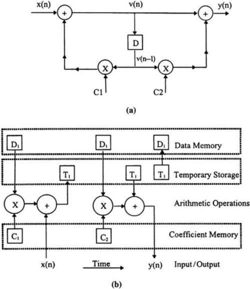
The simplest processor memory structure is a single bank of memory, which the processor accesses through a single set of address and data lines, as shown in Figure 5-9. This structure, which is common among non-DSP processors, is often considered a von Neumann architecture. Both program instructions and data are stored in the single memory. In the simplest (and most common) case, the processor can make one access (either a read or a write) to memory during each instruction cycle.
If we consider programming a simple von Neumann architecture machine to implement the example FIR filter algorithm, the shortcomings of the architecture become immediately apparent. Even if the processor’s data path is capable of completing a multiply-accumulate operation in one instruction cycle, it will take four instruction cycles for the processor to actually perform the multiply-accumulate operation, since the four memory accesses outlined previously must proceed sequentially, with each memory access taking one instruction cycle. This is one reason why conventional processors often do not perform well on DSP-intensive applications and why designers of DSP processors have developed a wide range of alternatives to the von Neumann architecture, which we explore next.
The previous discussions indicate that parallel memories are preferred in DSP applications. In most DSPs, Harvard architecture coexists with data pipelines and instruction processors in a very efficient manner. The systems with specific addressing modes for signal processing applications could be best described as special instruction set computers (SISC). SISC architecture is characterized by a memory-oriented special purpose instruction set.
5.4.3.1 Basic Harvard Architecture
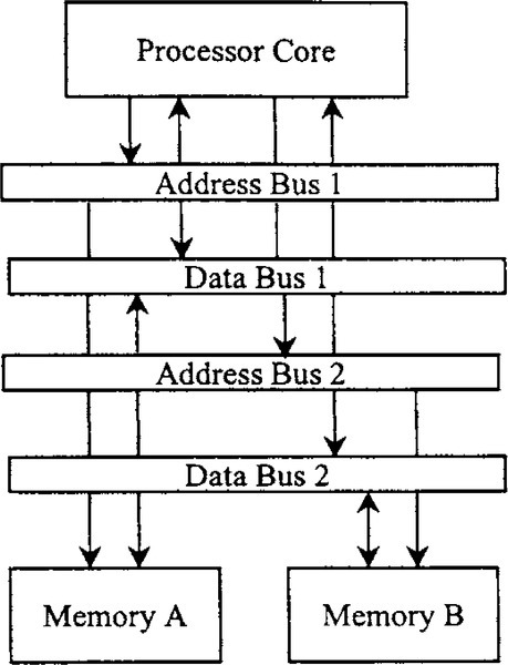
Harvard architecture refers to a memory structure in which the processor is connected to two independent memory banks via two independent sets of buses. In the original Harvard architecture, one memory bank holds program instructions and the other holds data. Commonly, this concept is extended slightly to allow one bank to hold program instructions and data, while the other bank holds data only. This “modified” Harvard architecture is shown in Figure 5-10. The key advantage of the Harvard architecture is that two memory accesses can be made during any one instruction cycle. Thus, the four memory accesses required for the example FIR filter can be completed in two instruction cycles. This type of memory architecture is used in many DSP families including the Analog Devices ADSP21xx.
5.4.3.2 SISC Architecture
While microprocessors are based on register-oriented architecture, signal processors have memory-oriented architectures. Multiple memories for both program and data have been present even in the first-generation DSPs such as TMS320C10. Modern DSPs have as many as six parallel memories for the use of the instruction or the data processors. External memory is as easily accessible as internal memory. In addition, a rich set of addressing modes tailored for signal processing applications also are provided. We describe the architecture representative of SISC computers and expect that future generations of SISC computers will have communication primitives as part of the standard instruction set. The basic instruction cycle is a unit of time measurement in the context of signal processing architectures, in some sense, the average time required to execute an ALU instruction. The basic instruction cycle is further divided into subcycles (usually two to four). The memory cycle time is that required to access one operand from the memory. The high-memory bandwidth requirement in SISC computers can be met by either providing for memories with very low-memory cycle times or multiple memories with relatively slower cycle times. Typically, an instruction cycle is twice as long as a memory cycle for on-chip memory (and equal to the memory cycle for external memory). Clearly, this facilitates the use of operand fetch and execution pipelines of two-operand instructions with on-chip data memories. If parallel data memories are provided, then the total number of memory cycles per instruction cycle is increased. The total number of memory cycles possible within a single basic instruction cycle is defined as the demand ratio (Kogge, 1981) for a SISC machine. Higher demand ratios lead to a higher throughput of instructions:

5.4.3.3 Multiple Access Memory-Based Architecture
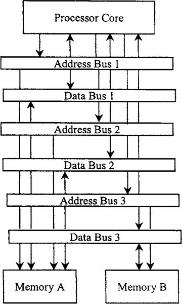
As discussed, Harvard architecture achieves multiple memory accesses per instruction cycle by using multiple, independent memory banks connected to the processor data path via independent buses. While a number of DSP processors use this approach, there are other ways to achieve multiple memory accesses per instruction cycle. These include using fast memories that support multiple, sequential accesses per instruction cycle over a single set of buses and using “multiported” memories that allow multiple concurrent memory accesses over two or more independent sets of buses.
Achieving increased memory access capacity by use of multiported memory is becoming popular with the development of memory technology. A multiported memory has multiple independent sets of address and data connections, allowing multiple independent memory access to proceed in parallel. The most common type of multiported memory is the dual-ported variety, which provides two simultaneous accesses. However, triple- and even quadruple-ported varieties sometimes are used. Multiported memories dispense with the need to arrange data among multiple, independent memory banks to achieve maximum performance. The key disadvantage of multiported memories is that they are much more costly (in terms of chip area) to implement than standard, single-ported memories. Some DSP processors combine a modified Harvard architecture with the use of multiported memories. The memory architecture shown in Figure 5-11, for example, includes a single-ported program memory with a dual-ported data memory. This arrangement provides one program memory access and two data memory accesses per instruction word and is used in the Motorola DSP561xx processors. For a more-detailed discussion of these techniques, see Lapsley et al. (1997).
5.4.4 Modifications to Harvard Architecture
The basic Harvard Architecture can be modified into six different types. This discussion is beyond the scope of the chapter and for details, see Lee (1988, 1989).
5.5 Special Addressing Modes
In addition to general addressing modes used in microprocessor systems, several special addressing modes are used in DSPs, including circular addressing and bit reversed addressing. For a comprehensive discussion on addressing modes, see Lapsley et al. (1997), as only circular addressing and bit reversed addressing are discussed here.
5.5.1 Circular Addressing
Many DSP applications need to manage data buffers. A data buffer is a section of memory used to store data that arrive from an off-chip source or a previous computation until the processor is ready to process the data. In realtime systems, where dynamic memory allocation is prohibitively expensive, the programmer usually must determine the maximum amount of data that a given buffer must hold and set aside a portion of memory for that buffer. The buffers generally use a first-in-first-out (FIFO) protocol, meaning that data values are read out of the buffer in the order in which they arrived.
In managing the movement of data into and out of the buffer, the programmer maintains two pointers, which are stored in registers or in memory: a read pointer and a write pointer. The read pointer points to (that is, contains the address of) the memory location containing the next data value to arrive, as illustrated in Figure 5-12. Each time a read or write operation is performed, the read or write pointer is advanced and the programmer must check to see whether the pointer has reached the last location in the buffer. When the pointer reaches the end of the buffer, it is reset to point to the first location in the buffer. Checking whether the pointer has reached the end of the buffer after each buffer operation and resetting it if it has is time consuming. For systems that use buffers extensively, this linear addressing can cause a significant performance bottleneck.
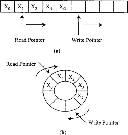
To address this bottleneck, many DSPs have a special addressing capability that allows them, after each buffer address calculation, to automatically check whether the pointer has reached the end of the buffer and reset it at the buffer start location if necessary. This capability is called modulo addressing or circular addressing.
The term modulo refers to modulo arithmetic, where numbers are limited to a specific range. This is similar to the arithmetic used in a clock, which is based on a 12-hour cycle. When the result of a calculation exceeds the maximum value, it is adjusted by repeatedly subtracting from it the maximum representable value until the result lies within the specified range. For example, four hours after 10 o’clock is 2 o’clock (14 modulo 12).
When modulo address arithmetic is in effect, read and write pointers (address registers) are updated using pre- or postincrement register-indirect addressing (Lapsley et al., 1997). The processor’s address generation unit performs modulo arithmetic when new address values are computed, creating the appearance of a circular memory layout, as illustrated in Figure 5-11(b). Modulo address arithmetic eliminates the need for the programmer to check the read and write pointers to see whether they have reached the end of the buffer and reset them once they have reached the end. This results in much faster buffer operations and makes modulo addressing a valuable capability for many applications.
In most real-time signal processing applications, such as those found in filtering, the input is an infinite stream of data samples. These samples are placed in “windows” and used in filtering applications. For instance, a sliding window of N data samples is used by an FIR filter with N taps. The data samples simulate a tapped-delay line and the oldest sample is written over by the most recent sample. The filter coefficients and the data samples are written into two circular buffers. Then, they are multiplied and accumulated to form the output sample result, which is stored. The address pointer for the data buffer is updated and the samples appear shifted by one sample period, the oldest data being written out and the most recent data is written into that location.
5.5.2 Bit-Reversed Addressing
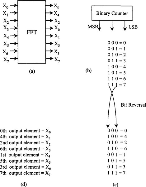
Perhaps the most unusual of addressing modes, bit-reversed addressing is used only in very specialized circumstances. Some DSP applications make heavy use of the fast Fourier transform (FFT) algorithm. The FFT is a fast algorithm for transforming a time-domain signal into its frequency-domain representation and vice versa (Oppenheim and Schafer, 1988; Kularatna, 1996, Chapter 9). However, the FFT has the disadvantage that it either takes its input or leaves its output in a scrambled order. This dictates that the data be rearranged to or from natural order at some point.
The scrambling required depends on the particular variation of the FFT. The radix-2 implementation of an FFT, a very common form, requires reordering of a particularly simple nature, bit-reversed ordering. The term bit reversed refers to the observation that, if the output values from a binary counter are written in reverse order (that is, least significant bit first), the resulting sequence of counter output values will match the scrambled sequence of the FFT output data. This phenomenon is illustrated in Figure 5-13.
Because the FFT is an important algorithm in many DSP applications, many DSP processors include special hardware in their address generation units to facilitate generating bit-reversed address sequences for unscrambling FFT results. For example, the Analog Devices ADSP-210xx provides a bit-reverse mode, which is enabled by setting a bit in a control register. When the processor is in the bit-reverse mode, the output of one of its address registers is bit reversed before being applied to the memory address bus.
An alternative approach to implementing bit-reversed addressing is the use of reverse-carry arithmetic. With reverse-carry arithmetic, the address generation unit reverses the direction in which carry bits propagate when an increment is added to the value in an address register. If reverse-carry arithmetic is enabled in the AGU and the programmer supplies the base address and increment value in bit-reversed order, then the resulting addresses will be in bit-reversed order. Reverse-carry arithmetic is provided in the AT&T DSP32xx, for example.
5.6 Important Architectural Elements in a DSP
Based on the preceding chapter’s discussion on microprocessors, it may be relevant for us to discuss special function blocks in a DSP chip. Performing efficient digital signal processing on a microprocessor is a tricky business. Although the ability to support single-cycle multiplier/accumulators (MACs) is the most important function a DSP performs, many other functions are critical for real-time DSP applications. Executing a real-time DSP application requires an architecture that supports high-speed data flow to and from the computation units and memory through a multiport register file. This execution often involves the use of direct memory access units and address generation units that operate in parallel with other chip resources. Address generation units or AGUs, which perform address calculations, allow the DSP to bring two pieces of data per clock, which is a critical need for real-time DSP algorithms.
It is important for DSPs to have an efficient looping mechanism, because most DSP code is highly repetitive. The architecture allows for zero-overhead looping, in which no additional instructions are needed to check the completion of loop iterations. Generally, DSPs take looping a step further by including the ability to handle nested loops.
DSPs typically handle an extended precision and dynamic range to avoid overflow and minimize round-off errors. To accommodate this capability, DSPs generally include dedicated accumulators with registers wider than the nominal word size to preserve precision. DSPs also must support circular buffers to handle algorithmic functions, such as tapped delay lines and coefficient buffers. DSP hardware updates circular-buffer pointers during every cycle in parallel with other chip resources. During each clock cycle, the circular-buffer hardware performs an end-of-buffer comparison and resets the pointer with no overhead when it reaches the end of the buffer. FFTs and other DSP algorithms also require bit-reversed addressing.
5.6.1 Multiplier/Accumulator
The multiplier/accumulator provides high-speed multiplication, multiplication with cumulative addition, multiplication with cumulative subtraction, saturation, and clear-to-zero functions. A feedback function allows part of the accumulator output to be used directly as one of the multiplicands of the next cycle. To explain MAC operation, we take a real-life example from the ADSP21XX family (see Figure 5-14).
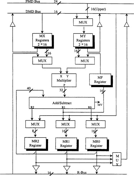
The multiplier has two 16-bit input ports, X and Y, and a 32-bit product output port, P. The 32-bit product is passed to a 40-bit adder/subtracter, which adds or subtracts the new product from the content of the multiplier result (MR) register or passes the new product directly to MR. The MR register is 40 bits wide. In this discussion, we refer to the entire register as MR, although it actually consists of three smaller registers: MR0 and MR1, which are 16 bits wide, and MR2, which is 8 bits wide.
The adder/subtracter is greater than 32 bits to allow for intermediate overflow in a series of multiply/accumulate operations. The multiply overflow (MV) status bit is set when the accumulator has overflowed beyond the 32-bit boundary; that is, when there are significant (nonsign) bits in the top nine bits of the MR register (based on two’s-complement arithmetic). The input/output registers of the MAC section are similar to the ALU. The X input port can accept data from either the MX register file or any register on the result (R) bus. The R bus connects the output registers of all the computational units, permitting them to be used directly as input operands. Two registers in the MX register file, MX0 and MX1, can be read and written from the data memory data (DMD) bus. The MX register file output is dual ported so that one register can provide input to the multiplier while the other one drives the DMD bus.
The Y input port can accept data from either the MY register file or the MF register. The MY register file has two registers, MY0 and MY1, which can be read and written from the DMD bus and written from the program memory data (PMD) bus. The ADSP-2101 instruction set also provides for reading these registers over the PMD bus but with no direct connection; this operation uses the DMD-PMD bus exchange unit. The MY register file output also is dual ported so that one register can provide input to the multiplier while either one drives the DMD bus.
The output of the adder/ subtracter goes to either the MF register or the MR register. The MF register is a feedback register that allows bits 16–31 of the result to be used directly as the multiplier Y input on a subsequent cycle. The 40-bit adder/subtracter register (MR) is divided into three sections: MR2, MR1, and MR0. Each register can be loaded directly from the DMD bus and its output sent to either the DMD bus or the R bus.
Any register associated with the MAC can be both read and written in the same cycle. Registers are read at the beginning of the cycle and written at the end of the cycle. A register read instruction, therefore, reads the value loaded at the end of a previous cycle. A new value written to a register cannot be read out until a subsequent cycle. This allows an input register to provide an operand to the MAC at the beginning of the cycle and be updated with the next operand from memory at the end of the same cycle. It also allows a result register to be stored in memory and updated with a new result in the same cycle.
The MAC contains a duplicate bank of registers, shown in Figure 5-14 behind the primary registers. There actually are two sets of MR, MF, MX, and MY register files. Only one bank is accessible at a time. The additional bank of registers can be activated for extremely fast context switching. A new task, such as an interrupt service routine, can be executed without transferring current states to storage. The selection of the primary or alternate bank of registers is controlled by bit 0 in the processor mode states register (MSTAT). If this bit is 0, the primary bank is selected; if it is 1, the secondary bank is selected. For details, see Ingle and Proakis (1991) and New (1995).
5.6.2 Address Generation Units
Most DSP processors include one or more special address generation units dedicated to calculating addresses. Manufacturers refer to these units by various names. For example, Analog Devices calls its AGU a data address generator, and AT&T calls its a control arithmetic unit. An AGU can perform one or more complex address calculations per instruction cycle without using the processor’s main data path. This allows address calculations to take place in parallel with arithmetic operations on data, improving processor performance. The differences among address generation units are manifested in the types of addressing modes provided and the capability and flexibility of each addressing mode. As an example let us take data addressing units in the ADSP-21xx family.
5.6.2.1 Data Address Units of ADSP-21xx Family: An Example
Data address generator (DAG) units contain two independent address generators so that program and data memories can be accessed simultaneously. Let us discuss the operation of the DAGs taking the ADSP-2101 as an example. The DAGs provide indirect addressing capabilities and perform automatic address modification. In the ADSP-2101, the two DAGs differ: DAG1 generates data memory addresses and provides an optional bit-reversal capability, DAG2 can generate both data memory and program memory addresses but has no bit reversal.
Figure 5-15 shows a block diagram of a single DAG. There are three register files: the modify (M) register file, the index (I) register file, and the length (L) register file. Each file contains four 14-bit registers that can be read from and written to via the DMD bus. The I registers (I0-3 in DAG1, I4-7 in DAG2) contain the actual addresses used to access memory. When data is accessed in the indirect mode, the address stored in the selected I register becomes the memory address. With DAG1, the output address can be bit reversed by setting the appropriate mode bit in the mode status register, as discussed next. Bit reversal facilitates FFT addressing.
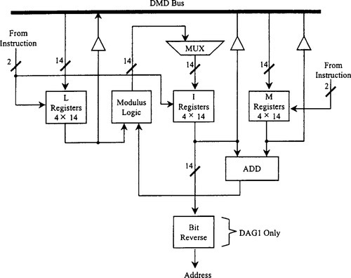
The data address generator employs a postmodification scheme. After an indirect data access, the specified M register (M0-3 in DAG2) is added to the specified I register to generate the new I value. The choice of the I and M registers is independent within each DAG. In other words, any register in the 10-3 set may be modified by any register in the M0-3 set in any combination but not by those in DAG2 (M4-7). The modification values stored in the M register are signed numbers so that the next address can be either higher or lower. The address generators support both linear and circular addressing. The value of the L register determines which addressing scheme is used. For circular buffer addressing, the L register is initialized with the length of the buffer. For linear addressing, the modulus logic is disabled by setting the corresponding L register to 0. L registers and I registers are paired and the selection of the L register (L0-3 in DAG1, L4-7 in DAG2) is determined by the I register used. Each time an I register is selected, the corresponding L register provides the modulus logic with the length information. If the sum of the M register content and the I register content crosses the buffer boundary, the modified I register value is calculated by the modulus logic using the L register value.
All data address generator registers (I, M, and L registers) are loadable and readable from the lower 14 bits of the DMD bus. Since the I and L register content is considered unsigned, the upper 2 bits of the DMD bus are padded with zeros when reading them. The M register content is signed; when reading an M register, the upper 2 bits of the DMD bus are sign extended. The modulus logic implements automatic pointer wraparound for accessing circular buffers. To calculate the next address, the modulus logic uses the following information:
• The current location, found in the I register (unsigned).
• The modify value, found in the M register (signed).
• The buffer length, found in the L register (unsigned).
• The buffer base address.
From such input, the next address is calculated using the formula
where
M = modify value (signed);
B = base address (generated by the linker);
L = buffer length M+;
I = modified address;
and M < L (which ensures that the next address cannot wrap around the buffer more than once in one operation).
5.6.3 Shifters
Shifting a binary number allows scaling. A shifter unit in a DSP provides a complete set of shifting functions, which can be divided into two categories: arithmetic and logical. A logical left shift by 1 bit inserts a 0 bit in the least significant bit, while a logical right shift by 1 bit inserts a 0 bit in the most significant bit. In contrast, an arithmetic right shift duplicates the sign bit (either a 1 or 0, depending on whether the number is negative or not) into the most significant bit. Although people use the term arithmetic left shift, arithmetic and logical left shifts really are identical: Both shift the word left and insert a 0 in the least significant bit.
Arithmetic shifting provides a way of scaling data without using the processor’s multiplier. Scaling is especially important in fixed-point processors, where proper scaling is required to obtain accurate results from mathematical operations.
Virtually all DSPs provide shift instructions of one form or another. Some processors provide the minimum; that is, instructions to do arithmetic left or right shifting by 1 bit. Some processors may provide instructions for 2- or 4-bit shifts. These can be combined with single-bit shifts to synthesize n-bit shifts, although at a cost of several instruction cycles.
Increasingly, many DSP processors feature a barrel shifter and instructions that use the barrel shifter to perform arithmetic or logical left or right shifts by any number of bits. Examples include the AT&T DSP16xx, the Analog Devices ADSP-21xx and ADSP-210xx, the DSP Group OakDSPCore, the Motorola DSP563xx, the SGS-Thompson D950-CORE, and the Texas Instruments TMS320C5x and TMS320C54x. If you start with a 16-bit input, a complete set of shifting functions needs a 32-bit output. These include arithmetic shift, logical shift, and normalization. The shifter also derives the exponent and common exponent for an entire block of numbers. These basic functions can be combined to efficiently implement any degree of numerical format control, including full floating point representation. Figure 5-16 shows a block diagram of the ADSP-2101.
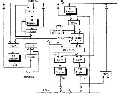
The variable shifter section in the ADSP-2100 can be divided into a shifter array, an OR/PASS logic, an exponent detector, and the exponent compare logic.
The shifter array is a 16 × 32 barrel shifter. It accepts a 16-bit input and can place it anywhere in the 32-bit output field, from off-scale right to off-scale left, in a single cycle. This gives 49 possible placements within the 32-bit field. The placement of the 16 input bits is determined by a control code (C) and a HI/LO reference signal.
The shifter array and its associated logic are surrounded by a set of registers. The shifter input (SI) register provides input to the shifter array and the exponent detector. The SI register is 16 bits wide and is readable and writable from the DMD bus. The shifter array and the exponent detector also take as inputs arithmetic, shifter, or multiplier results via the R bus. The shifter result (SR) register is 32 bits wide and divided into two 16-bit sections, SR0 and SR1. The SR0 and SR1 registers can be loaded from the DMD bus and sent to either the DMD bus or the R bus. The SR register also is fed back to the OR/PASS logic to allow double-precision shift operations. The SE (shifter exponent) register is 8 bits wide and holds the exponent during the normalize and denormalize operations. The SE register is loadable and readable from the lower 8 bits of the DMD bus. It is a two’s-complement, integer value.
The SB (shifter block) register is important in block floating point operations where it holds the block exponent value; that is, the value by which the block values must be shifted to normalize the largest value. SB is 5 bits wide and holds the most recent block exponent value. The SB register is loadable and readable from the lower 5 bits of the DMD bus. It is a two’s-complement, integer value.
Whenever the SE or SB registers are loaded onto the DMD bus, they are sign extended to a 16-bit value. Any of the SI, SE, or SR registers can be read and written in the same cycle. Registers are read at the beginning of the cycle and written at the end of the cycle. All register reads, therefore, read values loaded at the end of a previous cycle. A new value written to a register cannot be read out until a subsequent cycle. This allows an input register to provide an operand to the shifter at the beginning of the cycle and be updated with the next operand at the end of that cycle. It also allows a result register to be stored in memory and updated with a new result in the same cycle.
The shifter section contains a duplicate bank of registers, shown in Figure 5-16 behind the primary registers. There actually are two sets of SE, SB, SI, SR1, and SR0 registers, only one bank accessible at a time. The additional bank of registers can be activated for extremely fast context switching. A new task, such as an interrupt service routine, can be executed without transferring current states to storage. The selection of the primary or alternate bank of registers is controlled by bit 0 in the processor mode status register. If this bit is 0, the primary bank is selected; if it is 1, the secondary bank is selected.
The shifting of the input is determined by a control code (C) and a HI/LO reference signal. The control code is an 8-bit signed value that indicates the direction and number of places the input is to be shifted. Positive codes indicate a left shift (upshift) and negative codes indicate a right shift (downshift). The control code can come from three sources: the content of the shifter exponent register, the negated content of the SE register, or an immediate value from the instruction.
The HI/LO signal determines the reference point for the shifting. In the HI state, all shifts are referenced to SR1 (the upper half of the output field); and in the LO state, all shifts are referenced to SR0 (the lower half). The HI/LO reference feature is useful when shifting 32-bit values since it allows both halves of the number to be shifted with the same control code. HI/LO reference signal is selectable each time the shifter is used.
The shifter fills any bits to the right of the input value in the output field with zeros, and bits to the left are filled with the extension bit (X). The extension bit can be fed by three possible sources depending on the instruction being performed: the MSB of the input, the AC bit from the arithmetic status register, or a zero.
The OR/PASS logic allows the shifted sections of a multiprecision number to be combined into a single quantity. When PASS is selected, the shifter array output is passed through and loaded into the shifter result register unmodified. When OR is selected, the shifter array is bitwise ORed with the current contents of the SR register before being loaded there.
The exponent detector derives an exponent for the shifter input value. The exponent detector operates in one of three ways, which determine how the input value is interpreted. In the HI state, the input is interpreted as a single precision number or the upper half of a double precision number. The exponent detector determines the number of leading sign bits and produces a code that indicates how many places the input must be upshifted to eliminate all but one of the sign bits. The code is negative so that it can become the effective exponent for the mantissa formed by removing the redundant sign bits.
In the HI-extend state (HIX), the input is interpreted as the result of an add or subtract performed in the ALU section, which may have overflowed. Therefore, the exponent detector takes the arithmetic overflow (AV) status into consideration. If AV is set, then a + 1 exponent becomes output to indicate an extra bit is needed in the normalized mantissa (the ALU carry bit); if AV is not set, then HI-extend functions exactly like the HI state. When performing a derive exponent function in HI or HI-extend modes, the exponent detector also sends out a shifter sign (SS) bit, which is loaded into the arithmetic status register. The sign bit is the same as the MSB of the shifter input except when AV status is set; when AV status is set in the HI-extend state, the MSB is inverted to restore the sign bit of the overflow value. In the LO state, the input is interpreted as the lower half of a double precision number. In the LO state, the exponent detector interprets the SS bit in the arithmetic status register as the sign bit of the number. The SE register is loaded with the output of the exponent detector only if SE contains P15. This occurs only when the upper half—which must be processed first — contains all sign bits. The exponent detector output also is offset by P16 to indicate that the input actually is the lower half of a 32-bit value.
The exponent compare logic is used to find the largest exponent value in an array of shifter input values. The exponent compare logic in conjunction with the exponent detector derives a block exponent. The comparator compares the exponent value derived by the exponent detector with the value stored in the shifter block exponent register and updates the SB register only when the derived exponent value is larger than the value in the SB register.
Shifters in different DSPs have different capabilities and architecture. For example, the TMS320C25 scaling shifter shifts to the left from none to 16 bits. Two other shifters can shift data coming from the multiplier left 1 bit or 4 bits or can shift data coming from the accumulator left from none to 7 bits. These two shifters add the advantage of being able to scale data during the data move instead of requiring an additional shifter operation.
5.6.4 Loop Mechanisms
DSP algorithms frequently involve the repetitive execution of a small number of instructions, so-called inner loops or kernels. FIR and IIR filters, FFTs, matrix multiplication, and a host of other application kernels are performed by repeatedly executing the same instruction or sequence of instructions. DSPs have evolved to include features to efficiently handle this sort of repeated execution. To understand the evolution, we look at the problems associated with traditional approaches to related instruction execution. First, a natural approach to looping uses a branch instruction to jump back to the start of the loop.
Second, because most loops execute a fixed number of times, the processor must use a register to maintain the loop index; that is, the count of the number of times the processor has been through the loop. The processor’s data path must be used to increment or decrement the index and test to see if the loop condition has been met. If not, a conditional branch brings the processor back to the top of the loop. All of these steps add overhead to the loop and use precious registers.
DSPs have evolved to avoid these problems via hardware looping, also known as zero-overhead looping. Hardware loops are special hardware control constructs that repeat between hardware loops and software loops so that hardware loops lose no time incrementing or decrementing counters, checking to see if the loop is finished, or branching back to the top of the loop. This can result in considerable savings. To explain how a loop mechanism improves the efficiency, we once again use the ADSP-2101 as an example (see Figure 5-17).

The ADSP-2100A program sequencer supports zero overhead DO UNTIL loops. Using the count stack, loop stack, and loop comparator, the processor can determine whether a loop should terminate and the address of the next instruction (either the top of the loop or the instruction after the loop) with no overhead cycle.
A DO UNTIL loop may be as large as program memory size permits. A loop may terminate when a 16-bit counter expires or when any other arithmetic condition occurs. The following example shows a three-instruction loop that is to be repeated 100 times:
Do Label UNTIL CE
First instruction of loop
Second instruction of loop
Label: Last instruction of loop
First instruction outside loop
The first instruction loads the counter with 100. The DO UNTIL instruction contains the address of the last instruction in the loop (in this case the address represented by the identifier, Label) and the termination condition (in this case the count expiring, CE). The execution of the DO UNTIL instruction causes the address of the first instruction of the loop to be pushed on the program counter stack and the address of the last instruction of the loop to be pushed on the loop stack (see Figure 5-17).
As instruction addresses are sent to the program memory address bus and the instruction is fetched, the loop comparator checks to see if the instruction is the last instruction of the loop. If it is, the program sequencer checks the status and condition logic to see if the termination condition is satisfied. The program sequencer then either takes the address from the program counter stack (to go back to the top of the loop) or simply increments the program counter (to go to the first instruction outside the loop).
The looping mechanism of the ADSP-2100A is automatic and transparent to the user. As long as the DO UNTIL instruction is specified, all stack and counter maintenance and program flow is handled by the sequencer logic with no overhead. This means that, in one cycle, the last instruction of the loop is being executed and, in the very next cycle, the first instruction of the loop is executed or the first instruction outside the loop is executed, depending on whether the loop terminated or not. For further details of program sequencer and loop mechanisms of the ADSP-2100A, see Ingle and Proakis (1991) and Fine (•••).
5.7 Instruction Set
Generally, a DSP instruction set is tailored to the computation-intensive algorithms common to DSP applications. This is possible because the instruction set allows data movement between various computational units with minimum overhead. For example, sustained single-cycle multiplication/accumulation operations are possible.
Again, we use the ADSP-2101 as an example. The instruction set provides full control of the ADSP-2101’s three computation units: the ALU, MAC, and shifter. Arithmetic instructions can process single-precision 16-bit operands directly with provisions for multiprecision operations. The ADSP-2101 assembly language uses an algebraic syntax for arithmetic operations and data moves. The sources and destinations of computations and data moves are written explicitly, eliminating cryptic assembler mnemonics. There is no performance penalty for this; each program statement assembles into one 24-bit instruction, which executes in one cycle. There are no multicycle instructions in the ADSP-2101 instruction set. Some 50 registers surrounding the computational units are dual purpose, available for general purpose on-chip storage when not used in computation. This saves many memory access cycles and provides excellent freedom in coding. The control instructions provide conditional execution of most calculations and, in addition to the usual JUMP and CALL, support a DO UNTIL looping instruction. Return from Interrupt (RTI) and the Return from Subroutine (RTS) also are provided. These services are made compact and speedy by the single-cycle content save. The contents of the primary register set are held constant while the alternate set is enabled for subroutine and interrupt services. This eliminates the cluster of PUSHes and POPs of stacks common in general purpose microprocessors.
The ADSP-2101 also provides an IDLE instruction for idling the processor until an interrupt occurs. IDLE puts the processor into a low-power state while waiting for interrupts. Two addressing modes are supported for memory fetches. Direct addressing uses immediate values; indirect addressing uses the two data address generators.
The 24-bit instruction word allows a high degree of parallelism in performing operations. The instruction set allows for a single-cycle execution of any of the following combinations:
• Any ALU, MAC, or shifter operation (may be conditional).
• Any register-to-register move.
• Any data memory read or write.
• A computation with any data register/data register move.
• A computation with any memory read or write.
• A computation with a read from two memories.
The instruction set provides moves from any register to any other register or from most registers to and from either memory. For combining operations, almost any ALU, MAC, or shifter operation may be combined with any register-to-register moves or with a register move to or from either internal or external memory.
There are five basic categories of instruction: computational instructions, data move instructions, multifunction instructions, program flow control instructions, and miscellaneous instructions, all of which are described in the next several sections, with tables summarizing the syntax of each instruction category. The notation used in an instruction is shown in Table 5-1.
Table 5-1
Notation Used in the Instruction Set of the ADSP-21xx Family.
| Symbol | Meaning |
| +, − | Add, subtract |
| * | Multiply |
| a = b | Transfer into a the contents of b |
| , | Separates multifunction instruction |
| DM(addr) | The contents of data-meraory at location “addr” |
| PM(addr) | The contents of program memory at location “addr” |
| [option] | Anything within square brackets is an optional part of the instruction statement |
| |option a| | List of parameters enclosed by parallel vertical lines require the choice of one parameter from among the available list |
| CAPITAL LETTERS | Capital letters denote reserved words. These are instruction words, register names, and operand selections |
| Lower-case letters | Parameters are shown in small letters and denote an operand in the instruction for which there are numerous choices |
| < data > | These angle brackets denote an immediate data value |
| < addr > | These angle brackets denote an immediate value of an address to be coded in the instruction |
| ; | End of instruction |
(Reproduced by permission of Analog Devices, Inc.)
As it is beyond the scope of a chapter of this kind to explain the whole group of instructions, the computation instructions of the ADSP-2101 are described in a summary form. A more-detailed version instruction set can be found in Ingle and Proakis (1991) and the ADSP literature.
5.7.1 Computation Instructions: A Summary of the ADSP-21XX Family
The computation group executes all ALU, MAC, and shifter instructions. There are two functional classes: standard instructions, which include the bulk of the computation operations, can be executed conditionally (IF condition …), test the ALU status register, and may be combined with a data transfer in single-cycle multifunction instructions; and special instructions, which form a small subset and must be executed individually. Table 5-2 indicates permissible conditions for computation instructions, and Table 5-3 describes the computational input/output registers.
Table 5-2
Permissible Conditions for Computation Instructions of ADSP-2101.
| Condition | Keyword |
| ALU result is equal to zero | EQ |
| not equal to zero | NE |
| greater than zero | GT |
| greater than or equal to zero | GE |
| less than zero | LT |
| less than or equal to zero | LE |
| ALU carry status | |
| carry | AC |
| not carry | NOT AC |
| x-input sign: | |
| positive | POS |
| negative | NEG |
| ALU overflow status: | |
| overflow | AV |
| not overflow | NOT AV |
| MAC overflow status: | |
| overflow | MV |
| not overflow | NOT MV |
| Counter status: | |
| not expired | NOT CE |
[Reproduced by permission of Analog Devices, Inc.]
Table 5-3
Computational Input/Output Registers.
| Source for X input (xop) | Source for Y input (yop) | Destination* |
| ALU | ||
| AX0, AX1, AR | AY0, AY 1 | AR |
| MR0, MR1, MR2 | AF | AF |
| SR0, SR1 | ||
| MAC | ||
| MX0, MX1, AR | MY0, MY 1 | MR (MR2, MR1, MR0) |
| MR0, MR1, MR2 | MF | MF |
| SR0, SR1 | ||
| Shifter | ||
| SI, SR0, SR1 | SR (SR1, SR0) | |
| AR | ||
| MR0, MR1, MR2 |
[Reproduced by permission of Analog Devices, Inc.]
* Destination for output port R for ALU and MAC or destination for shifter output.
5.7.1.1 MAC Functions
Standard MAC instructions include multiply, multiply/accumulate, multiply/subtract, transfer AR conditionally, and clear. As an example, consider a MAC instruction for multiply/accumulate in the form:
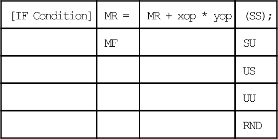
If the options MR and UU are chosen; if xop and yop are the contents of MXO and MYO, respectively; and if MAC overflow condition is chosen, then a conditional instruction would read
IF NOT MV MR = MR + MXO * MYO (UU);
The conditional expression, IF NOT MV, tests the MAC overflow bit. If the condition is not true, an NOP is executed. The expression MR = MR + MXO * MYO is the multiply/accumulate operation: The multiplier result register gets the value of itself plus the product of the X and Y input registers selected. The modifier selected in parentheses (UU) treats the operands as unsigned. Only one such modifier can be selected from the available set: (SS) means both are signed, (US) and (SU) mean that either the first or second operand is signed; (RND) means to round the (implicitly signed) result.
Accumulator saturation is the only MAC special function:
IF MV SAT MR;
The instruction tests the MAC overflow bit (MV) and saturates the MR register (for only one cycle) if that bit is set.
5.7.1.2 ALU Group Functions
Standard ALU instructions include add, subtract, logic (AND, OR, NOT, exclusive-OR), pass, negate increment, decrement, clear, and absolute value. The – function does two’s-complement subtraction while NOT obtains a one’s-complement. The PASS function passes the listed operand but tests and stores status information for later sign/zero testing. As an example, consider an ALU addition instruction for add/add-with-carry in the form
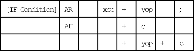
Instructions are in similar form for subtraction and logical operations. If the options AR and + yop + C are chosen, and if xop and yop are the contents of AXO and AYO, respectively, the unconditional instruction would read
AR = AXO + AYO + C;
This algebraic expression means that the ALU result register gets the value of the ALU x-input and y-input registers plus the value of the carry-in bit. This shortens the code and speeds execution by eliminating many separate register- move instructions.
When an optional IF condition is included, and if ALU carry bit status is chosen, then the conditional instruction would read
IF AC AR = AXO + AYO + C;
The conditional expression, IF AC, tests the ALU carry bit. If there is a carry from the previous instruction, this instruction executes; otherwise, an NOP occurs and execution continues with the next instruction.
Division is the only ALU special function. It is executed in two steps: DIVS computes the sign, then DIVQ computes the quotient. A full divide of a signed 16-bit divisor into a signed 32-bit quotient requires a DIVS followed by 15 DIVQs.
5.7.1.3 Shifter Group Functions
Shifter standard functions include arithmetic and logical shift as well as floating point and block floating point scaling operations, derive exponent, normalize, denormalize, and block exponent adjust. As an example, consider a shifter instruction for normalize:
IF NOT CE SR = OR NORM SI (HI);
The conditional expression, IF NOT CE, tests the “not counter expired” condition. If the condition is false, an NOP is executed. The destination of all shifting operations is the shifter result register. (The destination of the exponent detection instructions is SE or SB.) In this example, SI, the shifter input register, is the operand. The amount and direction of the shift are controlled by the signed value in the SE register in all shift operations except an immediate shift. Positive values cause left shifts; negative values cause right shifts.
The SR OR modifier (which is optional) logically ORs the result with the current contents of the SR register; this allows the user to construct a 32-bit value in SR from two 16-bit pieces. NORM is the operator and (HI) is the modifier that determines whether the shift is relative to the HI or LO (16-bit) half of SR. If SR OR is omitted, the result is passed directly into the SR.
Shift-immediate is the only shifter special function. The number of places (exponents) to shift is specified in the instruction word.
5.7.2 Other Instructions
Other instructions in a DSP could be grouped as in Table 5-4. The details could depend on the DSP family and hence Table 5-4 should be considered only a guideline.
Table 5-4
Instruction Set Groups (Using the ADSP 21 xx Family as an Example)
| Instruction Type | Purpose |
| Data move instructions | Move data to and from data registers and external memory |
| Multifunction instructions | Exploit the inherent parallelism of a DSP by combinations of data moves and memory writes/reads in a single cycle |
| Program flow control instructions | Directs the program sequence. In normal order, the sequence automatically fetches the next contiguous instruction for exertion. This flow can be altered by these instructions |
| Miscellaneous instruction | Such as NOP (no operation), PUSH/POP, and the like |
5.8 Development Systems
Although a development system is needed only initially (when the application is being designed) and not in the final product, a designer most likely will be working with development tools. Therefore, understanding the capabilities of these tools is as essential as understanding the architecture of the DSP itself.
The development process begins with the task of defining the target system hardware environment. The system builder is used to define the hardware environment. The system specification file includes the target hardware information. The system builder reads this file and creates an architecture description file that passes information about the target hardware to the linker, simulator, and emulator.
Code generation begins by creating assembly source code modules. An assembly module is a unit of source code, such as a calling program, subroutine, data buffer declaration section, or any combination. Each assembly code module is assembled separately by the assembler. Several modules then are linked to form an executable program.
The linker needs the target hardware information located in the architecture description file to determine placement of the code and data fragments. In the assembly modules, we have the option of specifying each code or data fragment as completely relocatable, relocatable within a defined memory segment, or placed at an absolute address. Absolute code or data modules are placed at the specified base address, provided the specified memory area has the correct attributes. Relocatable objects are placed in memory by the linker.
Using the architecture description file and the assembler output files, the linker determines the placement of relocatable code and data segments (including circular buffers) and places all segments in memory locations with the correct attributes (CODE or DATA, RAM or ROM). The linker generates an executable image file, which may be loaded into the simulator and emulator for debugging.
The simulator provides windows that display different aspects of the hardware environment. To replicate the target hardware environment, the simulator configures its memory according to the system builder output and simulates I/O ports according to user-entered simulator commands. This simulation provides the capability to debug the system and analyze performance before committing to a hardware prototype.
After debugging with the simulator, the emulator is used in the prototype target system to debug hardware, timing, and real-time software problems. It provides overlay memory to replace target system off-chip memory, including boot memory, if desired.
The PROM splitter translates the executable memory image file (linker output) into a file compatible with a PROM burner. Once the ADSP-2101 code is burned into PROM and an ADSP-2101 is plugged into the target board, the prototype is ready to run.
Figure 5-18(a) shows a flowchart of the ADSP-2101 development cycle. Figure 5-18(b) shows the system builder I/O. All the steps in the preceding development process except emulation are carried out by the software development system, while the hardware development consists of the emulator and the prototype target system.

5.9 Interface Between DSPs and Data Converters
Advances in semiconductor technology have given DSPs fast processing capabilities and data converter ICs have the conversion speeds to match the faster processing speeds. This section considers the hardware aspects of practical design.
5.9.1 Interface Between ADCs and DSPs
Precision sampling analog/digital converters generally have either parallel data output or a single serial output data link. We consider these separately.
5.9.1.1 Parallel Interfaces with ADCs
Many parallel output sampling ADCs offer three-state output that can be enabled or disabled using an output enable pin on the IC. While it may be tempting to connect the three-state output directly to a back plane data bus, severe performance-degrading noise problems will result. All ADCs have a small amount of internal stray capacitance between the digital output and the analog input (typically 0.1–0.5 μF). Every attempt is made during the design and layout of the ADC to keep this capacitance to a minimum. However, if there is excessive overshoot and ringing and possibly other high-frequency noise on the digital output lines (as would probably be the case if the digital output were connected directly to a back plane bus), this digital noise will couple back into the analog input through the stray capacitance. The effect of this noise would be to decrease the overall ADC SNR and ENOB. Any code-dependent noise also will tend to increase the ADC harmonic distortion.
The best approach to eliminating this potential problem is to provide an intermediate three-state output buffer latch located close to the ADC data output. This latch isolates the noisy signals on the data bus from the ADC data outputs, minimizing any coupling back into the ADC analog input.
The ADC data sheet should be consulted regarding exactly how the ADC data should be clocked into the buffer latch. Usually, a signal called conversion complete or busy from the ADC is provided for this purpose.
It also is a good idea not to access the data in the intermediate latch during the actual conversion time of the ADC. This practice will further reduce the possibility of corrupting the ADC analog input with noise. The manufacturer’s data sheet timing information should indicate the most desirable time to access the output data.
Figure 5-19 shows a simplified parallel interface between the AD676–16 bit, 100 kSPS ADC (or the AD7884) and the ADSP-2101 microcomputer. (Note that the actual device pins shown have been relabeled to simplify the following general discussion. In a real-time DSP application (such as in digital filtering), the processor must complete its series of instructions within the ADC sampling interval. Note that the entire cycle is initiated by the sampling clock edge from the sampling clock generator. Even though some DSP chips offer the capability to generate lower-frequency clocks from the DSP master clock, the use of these signals as precision sampling clock sources is not recommended due to the probability of timing jitter. It is preferable to generate the ADC sampling clock from a well-designed low noise crystal oscillator circuit as has been previously described.
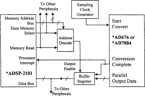
The sampling clock edge initiates the ADC conversion cycle. After the conversion is completed, the ADC conversion complete line is asserted, which in turn interrupts the DSP. The DSP places the address of the ADC that generated the interrupt on the data memory address bus and asserts the data memory select line. The read line of the DSP then is asserted. This enables the external three-state ADC buffer register outputs and places the ADC data on the data bus. The trailing edge of the read pulse latches the ADC data on the data bus into the DSP internal registers. At this time, the DSP is free to address other peripherals that may share the common data bus.
Because of the high-speed internal DSP clock (50 MHz for the ADSP- 2101), the width of the read pulse may be too narrow to access properly the data in the buffer latch. If this is the case, adding the appropriate number of programmable software wait states in the DSP will both increase the width of the read pulse and cause the data memory select and the data memory address lines to remain asserted for a correspondingly longer period of time. In the case of the ADSP-2101, one wait state is one instruction cycle, or 80 ns.
5.9.1.2 Interface Between Serial Output ADCs
ADCs that have a serial output (such as the AD677, AD776, and AD1879) have interfaces to the serial port of many DSP chips, as shown in Figure 5-20.
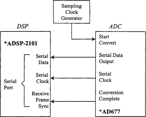
The sampling clock is generated from the low-noise oscillator. The ADC output data is presented on the serial data line one bit at a time. The serial clock signal from the ADC is used to latch the individual bits into the serial input shift register of the DSP serial port. After all the serial data are transferred into the serial input register, the serial port logic generates the required processor interrupt signal. The advantages of using serial output ADCs are a reduction in the number of interface connections as well as reduced noise because fewer noisy digital program counter tracks are close to the converter. In addition, SAR and Σ-Δ ADCs are inherently serial-output devices. The number of peripheral serial devices permitted is limited by the number of serial ports available on the DSP chip.
5.9.2 Interfaces with DACs
5.9.2.1 Parallel Input DACs
Most of the principles previously discussed regarding interfaces with ADCs also apply to interfaces with DACs. A generalized block diagram of a parallel input DAC is shown in Figure 5-21(a). Most high-performance DACs have an internal parallel DAC latch that drives the actual switches. This latch deskews the data to minimize the output glitch. Some DACs designed for real-time sampling data DSP applications have an additional input latch so that the input data can be loaded asynchronously to the DAC latch strobe. Some DACs have an internal reference voltage that can be either used or bypassed with a better external reference. Other DACs require an external reference.
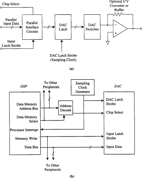
The output of a DAC may be a current or a voltage. Fast-video DACs generally are designed to supply sufficient output current to develop the required signal levels across resistive loads (generally 150 Ω, corresponding to a 75 Ω source and load-terminated cable). Other DACs are designed to drive a current into a virtual ground and require a current-to-voltage converter (which may be internal or external). Some high-impedance voltage-output DACs require an external buffer to drive reasonable values of load impedance.
A generalized parallel DSP-to-DAC interface is shown in Figure 5-21(b). The operation is similar to that of the parallel DSP-to-ADC interface described earlier. In most DSP applications, the DAC is operated continuously from a stable sampling clock generator external to the DSP. The DAC requires double-buffering because of the asynchronous interface to the DSP. The sequence of events as follows. Asserting the sampling clock generator line clocks the word contained in the DAC input latch into the DAC latch (the latch that drives the DAC switches). This causes the DAC output to change to the new value. The sampling clock edge also interrupts the DSP, which then addresses the DAC, enables the DAC chip select, and writes the next data into the DAC input latch using the memory write and data bus lines. The DAC now is ready to accept the next sampling clock edge.
5.9.2.2 Serial Input DACs
A block diagram of a typical serial input DAC is shown in Figure 5-22(a). The digital input circuitry consists of a serial-to-parallel converter driven by a serial data line and a serial clock. After the serial data is loaded, the DAC latch strobe clocks the parallel DAC latch and updates the DAC switches with a new word. Interface between DSPs and serial DACs is quite easy using the DSP serial port (Figure 5-22(b)). The serial data transfer process is initiated by the assertion of the sampling clock generator line. This updates the DAC latch and causes the serial port of the DSP to transmit the next word to the DAC using the serial clock and the serial data line.
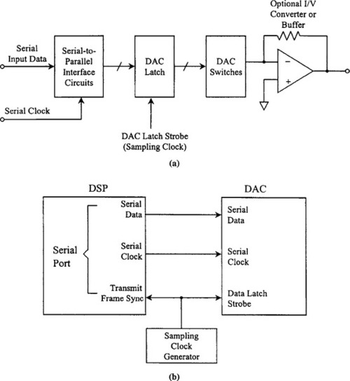
5.10 Practical Components and Recent Developments
During 1997 and 1998, incredible developments took place in the DSP components world. Vendors were focusing on several key aspects of the DSP architecture. The most obvious architectural improvements were in the increased “parallelism”: the number of operations the DSP can perform in an instruction cycle. An extreme example of parallelism is Texas Instruments’ C6x very-long-instruction-word (VLIW) DSP with eight parallel functional units. Although Analog Devices’ super Harvard architecture (SHARC) could perform as many as seven operations per cycle, the company and other vendors were working feverishly to develop their own VLIW-ized DSPs. In contrast to superscalar architectures, VLIW simplifies a DSP’s control logic by providing independent control for each processing unit. During 1997 the following important developments were achieved (Levy, 1997):
• While announcing the first general purpose VLIW DSP, Texas Instruments also announced the end of the road for the C8x DSP family. The company emphasized the importance of the compilers for DSPs with the purchase of DSP-compiler company Tartan.
• Analog Devices broke the $100 price barrier with its SHARC floating-point architecture.
• Lucent Technologies discontinued new designs incorporating its 32-bit, floating-point DSP. The company also focused its energy on application-specific rather than general purpose DSPs. The application-specific products target modems and other communication devices.
• Motorola’s DSP Division became the Wireless Signal Processing Division, although the company still supports many general purpose DSP and audio applications.
Among the hottest architectural innovations during 1998 was the move to dual multiply/accumulate units. The architecture of these MACs allows performing twice the digital/signal processing as before. TI kicked off this evolution with its VLIW-based C6x. Meanwhile, engineers designing with DSPs need a simple method to compare processor performance. Unfortunately, as types of processor architecture diversify, traditional metrics such as MIPS and MOPS have become less relevant. Alternatively, Berkeley Design Technology (BDTI, www.bdit.com) has become well known in the DSP industry for providing DSP benchmarks. Instead of using full-application benchmarks, BDTI has adopted a benchmark methodology based on DSP-algorithm kernels, such as FFTs and FIR filters. BDTI implements its suite of 11 kernel-based benchmarks on a variety of processors. You can find the results of these benchmarks in the company’s Buyer’s Guide to DSP Processors at Berkeley’s web site.
To see the developments over the past ten years, compare Cushman (1987) with Levy (1997, 1998b).