
Voltage References and Voltage Regulators
1.1 Introduction
Almost all electronic systems utilize a regulated power supply as an essential requirement. Most systems need a precision voltage reference as well. In the past, the task of voltage regulation was tediously accomplished with discrete devices. Today, with integrated circuit voltage references and regulators, this task has been significantly simplified. Not only can an extremely high precision be obtained, but also an extremely high degree of temperature stability.
The performance of today’s electronic devices such as microprocessors, test and measuring instruments, and sophisticated portable and handheld equipment is directly related to the quality of the supply voltage. This results in the need for tight regulation, low noise, and excellent transient response. The designer now has a wide choice of fixed, adjustable, and tracking voltage regulators, with many also incorporating built-in protection features.
One of the fastest growing markets in the world of power regulation is for switching regulators. These offer designers several important advantages over linear regulators, the most significant being size and efficiency. In addition, the ability to perform step-up, step-down, or voltage inverting functions is an attractive feature.
The old linear regulator is not totally out of business. The proliferation of battery-powered equipment in recent years has accelerated the development and usage of low-dropout (LDO) voltage regulators. Compared to a standard linear regulator, the LDO regulator using PNP transistors can maintain its output in regulation with a much lower voltage across it. While the NPN transistor requires about 2 V of headroom voltage to regulate, the LDO typically will work with less than 500 mV of input-to-output voltage differential. This reduced input voltage requirement is advantageous in battery-powered systems, since it translates directly into fewer battery cells (Simpson, 1996). In low-dropout applications, the efficiency advantage of switching regulators no longer is as great. A linear regulator design on the other hand offers several desirable features, such as low output noise and wide bandwidth, resulting in excellent transient response.
This chapter describes the basics of voltage references, linear and switching regulators, and continues to discuss the state-of-the-art components available, the advantages and disadvantages of different types of devices, their application environments as well as the basics of regulator design using these components.
1.2 Voltage References
1.2.1 Voltage Reference Fundamentals
A wide variety of voltage references are available today. However, all base their performance on the action of either a zener diode or a bandgap cell. Additional circuitry is included to obtain good temperature stability. Although discrete zener diodes are available in voltage ratings as low as 1.8 V to as high as 200 V, with power handling capabilities in excess of 100 W, their tolerance and temperature characteristics are unsuitable for many applications. Therefore, discrete zener diode-based references have additional circuitry to improve performance. The most popular reference is probably the temperature-compensated zener diode, particularly, for voltages above 5 V.
The operation of a bandgap reference is based on specific characteristics of diodes operating at the same current but different current densities. Bandgap references are available with output voltage ratings of about 1.2 to 10 V. The principal advantage of these devices is their ability to provide stable low voltages, such as 1.2, 2.5, or 5 V. However, bandgap references of 5 V and higher tend to have more noise than equivalent zener-based references. This is because, in bandgap references, higher voltages are obtained by amplification of the 1.2 V bandgap voltage by an internal amplifier. Their temperature stability also is below that of zener-based references.
1.2.2 Types of Voltage References
1.2.2.1 Zener-Based Voltage References
Zener diodes are semiconductor PN junction diodes with controlled reverse-bias properties, which make them extremely useful as voltage references. The V-I characteristics of an ideal zener diode is shown in Figure 1–1 (a) and a simple regulator circuit based on it in Figure 1-1 (b).
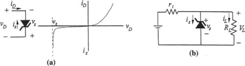
The reverse characteristics show that, at the breakdown point, the knee voltage is independent of the diode current. This knee voltage or the zener voltage is controlled by the amount of doping applied in the manufacturing process. In the simple regulator circuit shown in Figure 1–1 (b), as long as the zener diode is in its regulating range, the load voltage VL remains constant and equal to the nominal zener voltage, even when the input voltage and the load resistance varies over a wide range. If the input voltage increases, the diode maintains a constant voltage across the load by absorbing the extra current and keeping the load current constant. If the load resistance decreases, the extra current required to keep the load voltage constant is facilitated by a decrease in the current drawn by the zener diode.
In the preceding simplified analysis, the temperature dependence of the zener voltage was not taken into account. The stability of the output with temperature is a prime requirement of a voltage reference. Not only does the zener voltage vary with temperature, its variation also depends on the type of breakdown that occurs.
A zener diode has two distinctly different breakdown mechanisms: zener breakdown and avalanche breakdown. The zener breakdown voltage decreases as the temperature increases, creating a negative temperature coefficient (TC). The avalanche breakdown voltage increases with temperature (positive TC) (Pryce, 1990). This is illustrated in Figure 1–2. The zener effect and the avalanche effect dominate at low and high currents, respectively.
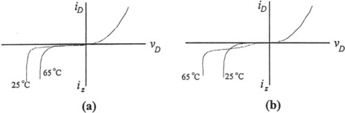
Although, theoretically, it is possible to select the operating point of a zener diode so that the two temperature coefficients will cancel out each other, in practical IC zener-based voltage references, a conventional forward-biased diode is used in series with a zener operating in the avalanche mode. A forward-biased diode has a negative TC, and this cancels the positive TC of the zener diode.
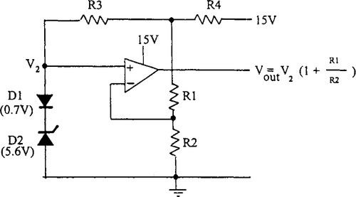
A simple zener-based voltage reference IC is shown in Figure 1–3. In this circuit, R4 provides the startup current for the diodes, thus setting the positive input of the op amp at V2. R3 sets the desired bias current for the diodes. Manufacturers set the output voltage to a value different from that of V2 through the ratio R1 to R2. By trimming this resistor ratio, the output voltage can be set to the desired accuracy. Also, by trimming R3, the bias current can be optimized to a point where a minimum TC is obtained.
TC specifications as low as 1 ppm/°C are possible with zener-based voltage reference ICs (Pryce, 1990).
1.2.2.2 Bandgap References
Similar to zener-based references, bandgap references also produce the sum of two voltages having opposite temperature coefficients. One voltage is the forward voltage of a conventional diode (the base-emitter junction of a transistor), which has a negative temperature coefficient. The other is the difference between the forward voltages of two diodes with the same current but operating at two current densities. A circuit diagram of a bandgap reference is shown in Figure 1–4.
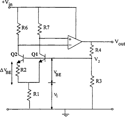
Transistors Q1 and Q2 are operating at the same current, but at different current densities. This is achieved by fabricating Q2 with a larger emitter area than Ql. Therefore, the base-emitter voltages of the two transistors are different. This difference is dropped across R2.
Extrapolated to absolute 0, VBE is equal to 1.205 V, the bandgap voltage of silicon, and has a predictable, negative temperature coefficient of –2 mV/°C. By adding a voltage to VBE, which has a positive temperature coefficient, a bandgap reference, at least theoretically, can generate a constant voltage at any temperature.
The base-emitter voltage difference is given by
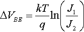
Where J1 and J2 are the current densities of transistor Q1 and Q2, respectively. Since the sum of the two transistor currents flow through R1, the voltage across R1 can be expressed as
Also,
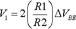
Usinig 1.2 and 1.3,

Therefore, V2 is the sum of VBE and the scaled ∆VBE Knapp (1998) shows that, if the emitter areas of the two transistors is eight, the temperature coefficients of VBE and ∆VBE cancel each other. The op amp raises the bandgap voltage V2 to a higher voltage at the output of the reference.
Bandgap references typically provide voltages ranging from 1.2 to 10 V. The advantage of bandgap references is their ability to provide voltages below 5 V. The greatest appeal of bandgap devices is the ability to function with operating currents from milliamps down to microamps.
IC bandgap references have additional features such as multiple calibrated voltages. Because most bandgap references are constructed in monolithic form, they are relatively inexpensive. However, their temperature coefficient is inferior to that of zener-based references. This is due to the second-order dependencies of Δ VBE on temperature.
1.2.3 Quality Measures of Voltage References
An ideal voltage reference would have the exact specified voltage, and it would not vary with time, temperature, input voltage, or load conditions. However, as it is impossible to fabricate such ideal references, manufacturers provide specifications informing the user of the device’s important quality parameters.
1.2.3.1 Output Voltage Error
This is the initial untrimmed accuracy of the reference at 25°C at a specified input voltage. This is specified in millivolts or a percentage. Some references provide pin connections for trimming their initial accuracy with an external potentiometer.
1.2.3.2 Temperature Coefficient
The temperature coefficient of a reference is its average change in output voltage as a function of temperature compared with its value at 25°C. This is specified in ppm/°C or mV/°C.
1.2.3.3 Line Regulation
This is the change in output voltage for a specified change in input voltage. Usually specified in %/V or μV/V of input change, line regulation is a measure of the reference’s ability to handle variations in supply voltage.
1.2.3.4 Load Regulation
This is the change in output voltage for a specified change in load current. Specified in μV/mA, %mA, or ohms of DC output resistance, load regulation includes any self-heating effects due to changes in power dissipation with load current.
1.2.3.5 Long-Term Stability
This is the change in the output voltage of a reference as a function of time. Specified in ppm/1000 hours at a specific temperature, the long-term stability is difficult to quantify. As a result, manufacturers usually provide only typical specifications, based on device data collected during the characterization process.
1.2.3.6 Noise
Although the preceding are the most important quality parameters of a voltage reference, noise is particularly of importance in certain applications such as A/D or D/A converters. In such applications, the noise from the reference should be less than 10% of the LSB value of the converter. Therefore, the higher the resolution of the converter, the lower should be the noise generated from the reference.
Noise depends on the operating current of the reference and generally is specified over a particular bandwidth and for a particular current. The specified band widths are 0.1–10 Hz (low-frequency noise) and 10 Hz-10 kHz (high- frequency noise).
1.2.4 Voltage Reference ICs
The levels of sophistication and pricing for voltage references range from simple and inexpensive to complex and costly. Devices are available for almost any conceivable application. Manufacturers of voltage references include National Semiconductor, Motorola, Analog Devices, Linear Technology, SGS-Thompson, Maxim Integrated Circuits, Texas Instruments, Precision Monolithic, and Silicon General.
1.2.4.1 Zener-Based References
Zener-based references usually are used in analog circuits that operate from 12–15 V supplies. Some zener-based voltage references are illustrated in Table 1–1.
Table 1-1
Illustrative Zener-Based References
| Device | Voltage (V) | Opening current | Accuracy | TC | Niose μV P-P (0.1 – 10 HZ) |
| REF101 (Burr-Brown) | 10 | 6 mA max | 5 mV | 1 ppm/°C | 6 |
| AD688 (Analog Devices) | + 10 and -10(tracking) | 9 mA | 5 mV | 2 ppm/°C | 6 |
| MAX2701 (Maximum Integrated Circuits) | –10 | 5 mA | 2.5 mV | 3 ppm/°C | 6 |
| LTZ1000 (Linear Technology) | 7.2 | 5 mA | 4 mV | 0.05 ppm/°C | 1.2 |
| LT1021 | 5,7,10 | 0.8 mA | 0.05% | 2 ppm/°C | 3 |

A typical high-performance zener diode is the REF101 from Burr-Brown with a reference voltage of 10 V (Burr-Brown, 1989). The combination of its excellent parameters makes this device well suited for use with high-resolution A/D and D/A converters or as a precision calibrated voltage standard. This device has a very high accuracy of 0.005 V and a temperature drift of 1 ppm/°C.
Analog Devices offers a wide range of both zener-based and bandgap precision references as part of its line of data conversion products. The zener-based AD688 is a high-precision + 10 and –10 V tracking reference. This device includes the basic reference cell and three additional amplifiers. The amplifiers are laser trimmed for low offset and low drift and maintain the accuracy of the reference. Low initial error and low temperature drift give the AD688 reference absolute ± 10 V accuracy performance in monolithic form.
The AD689, an 8.192 V reference, bridges the gap between 5 V and 10 V products. This device is especially useful in data conversion circuits that operate over ± 12 V but may swing over a 10% range.
The MAX2700 series (MAX2700/2701/2710) of 10 V references finds typical applications in high-resolution A/D and D/A systems and in data acquisition systems. The MAX2701 in this family is a –10 V reference.
The LTZ1000 from Linear Technology is an ultrastable reference operating at 7.2 V. This includes a heater resistor for temperature stabilization and a temperature sensing transistor, which results in very good temperature stability. Typical applications of this device are in voltmeters, calibrators, standard cells, scales, and low-noise RF oscillators (Linear Technology Corp., 1990).
The LT1021 is a precision reference available in three voltages: 5, 7, and 10. These devices are intended for circuits requiring a precise 5 V or 10 V reference with very low initial tolerance.
1.2.4.2 Bandgap References
Some illustrative bandgap references are illustrated in Table 1–2.
Table 1-2
Illustrative Bandgap References
| Device | Voltage (V) | Operating Current | Accuracy | Temperature stability | Noise (Typical) |
| LM136 | 2.5 | 400 μA-10 mA | 1% | 12 mV max form –55 to + 125 °C | NA |
| REF1004–1.2 | 1.2 | 10 μA min | 4 mV | 20 ppm/°C | 60 μV RMS (10 Hz-10 kHz) |
| LT1019–2.5 | 2.5 | 0.5 mA | 0.02% | 5 ppm/°C | Ppm P-P (0.1 – 10 Hz) |
| LTI034–1.2 | 1.2 | 10 μA | 1% | 20 ppm/°C | 4 μV P-P (0.1 – 10 Hz) |
| MAX675 | 5.0 | 1.4 mA max | 0.15 | 12 ppm/°C max | 10 μV P-P (0.1 – 10 Hz) |
| MAX872 | 2.5 | 10 μA max | 0.2 | 40 ppm/°C max | 60 μV P-P (0.1 – 10 Hz) |
| MAX676/767/768 | 4.096, 5, 10 | 10 mA max | 0.02 | 1 ppm/°C max over –40 to + 85 °C | 1.2 μV P-P (0.1 – 10 Hz) |
| LM385–2.5 | 2.5 | 8 μA min | 1 | 20 ppm/°C | 120 μV RMS (10 Hz– 10 KHz) |

Typical of the lower-cost, general-purpose bandgap references is the LM136 series from National Semiconductor. The LM136 and 336 are bandgap references with an output voltage of 2.5 V and an accuracy of 1–2%. These are particularly useful in obtaining a stable reference from a 5 V logic supply. Typical applications of this series are in digital voltmeters, power supply monitors, and the like (Linear Technology Corp., 1990). The REF-03 from Precision Monolithics is a low-cost, 2.5 V bandgap reference. Silicon General’s SG103 series of bandgap references is available in 13 voltage ratings, ranging from 1.8–5.6 V. The LT1019 from Linear Technology is an accurate bandgap reference, available in voltage ratings of 2.5, 4.5, 5, and 10 V. Applications for this device include A/D and D/A converters and precision regulators (Linear Technology Corp., 1990).
Maxim Integrated Circuits produces a wide range of references. One such series, the MAX676/677/678 produces + 4.096, 5, and 10 V calibrated, low-drift precision voltage references. One feature of the 4.096 low-dropout reference is that it operates from a 5 V ± 10% supply (Maxim Integrated Circuits, 1995). This series of references has excellent line and load regulation in addition to temperature stability. These devices find applications in high-resolution 16-bit A/D and D/A converters, precision test and measurement systems, high-accuracy transducers, and as calibrated voltage reference standards.
Micro-power voltage references, which consume as little as 10 μΑ operating current, are available, unlike zener-based references, which consume much larger currents. One such example is MAX872. Another micro-power reference, the MAX6120, draws a maximum current of 70 μΑ and operates over a 2.4–11 V input range. This is ideally suited for battery-powered systems and portable applications such as data acquisition systems (Maxim Integrated Circuits, 1996). The LM385 series of micro-power precision references operate at currents in the range of 15–20 μΑ.
The LT1034 micro-power precision reference from Linear Technology combines a 1.2 or 2.5 V bandgap reference with a 7 V zener-based auxiliary reference in a single package. The 1.2 V/2.5 V reference is a trimmed, bandgap voltage reference with 1% initial tolerance and guaranteed 20 ppm/°C temperature drift. Operating on only 10 μΑ, the LT1034 offers guaranteed drift and good long-term stability. The 7 V reference is a subsurface zener device for less demanding applications (Linear Technology Corp., 1990). The REF1004-1.2 and REF1004-2.5 are two terminal micro-power bandgap references designed for high accuracy with outstanding temperature characteristics at low operating currents. The REF1004 is a cost-effective solution when reference voltage accuracy, low power, and long-term temperature stability are required (Burr-Brown, 1993).
1.2.5 Design Basics
Some basic design tips as well as some facilities available in voltage reference ICs are illustrated in Figure 1-5, using the MAX873 as an example (Maxim Integrated Circuits, 1994). Figure 1-5(a) shows a typical application circuit with input and output bypassing for best transient performance. Figure 1-5(b) shows an output voltage trimming circuit. Although large adjustments of the output voltage may degrade its temperature performance, adjusting the output over a small range about the nominal output voltage is possible with most reference ICs.
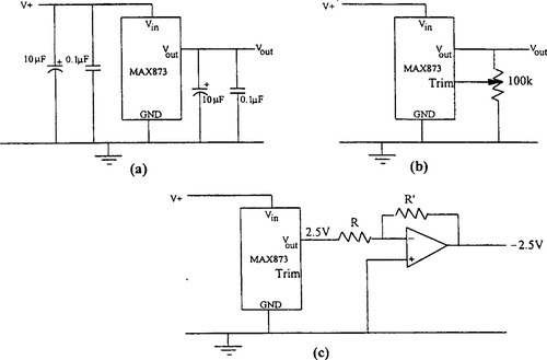
The generation of negative reference voltages is shown in Figure 1-5(c). An op amp in an inverting configuration is used, and the accuracy of the output depends on the matching of the two resistors R and R'.
1.3 Linear Regulators
1.3.1 Linear Regulator Fundamentals
Figure 1-6 illustrates the basic elements of a linear regulator. The output is regulated by controlling the voltage drop across the series-pass element, a power transistor biased in the linear region. The output voltage is maintained at a constant level by changing the voltage drop across this device.
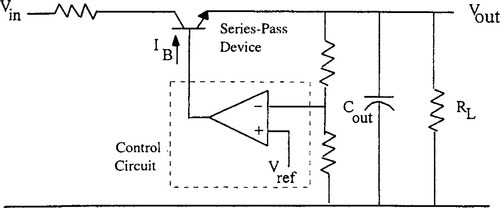
The control circuit detects the output voltage, and changes the on-resistance of the series-pass power transistor by changing its base current to keep the output voltage constant. The power dissipation in the linear regulator is a function of the difference between the input and the output voltages, output current, output driver power, and the quiescent controller power. The power dissipation in the series-pass device contributes largely to lower the efficiency of linear regulators compared to switching regulators. However, this disadvantage is insignificant in low-dropout linear regulators, which find many applications in today’s sophisticated electronic and communication equipment.
A major advantage of linear regulators in comparison with switching regulators is their low noise.
1.3.1.1 The Series-Pass Device
The power device selected to provide the pass function must be capable of operating under very low differential input/output voltages while providing reasonable efficiency. Pass devices typically are bipolar transistors or power MOSFETs.
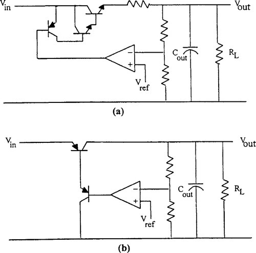
The first linear regulators had NPN Darlington transistors as the series-pass element. However, for low-dropout requirements, PNP transistors are more suitable, as they can maintain output regulation with very little voltage drop across it (Lee, 1989; Simpson, 1996). The dropout voltage of the linear regulator is defined as the input-output voltage differential at which the circuit ceases to regulate against further reduction in input voltage (National Semiconductor Corp., 1987).
As the output requirements of the regulator grow, the gain of suitable PNP power transistors decrease, resulting in excessive base current losses. Therefore, N-channel MOSFETs are a popular choice due to their low drive current, low on-resistance and cost. Recent advances in semiconductor technology have resulted in low on-resistance P-channel devices as well. The low drive current requirement of MOSFETs reduces the quiescent current of the regulator considerably which is a major advantage of these devices. The characteristics of the series-pass device determine what the differential input/output voltage limitations are and how much quiescent power is required by the regulator. Figure 1-7 shows the use of NPN Darlington and PNP transistors as the series-pass element in linear regulators. A comparison of NPN and PNP transistors with several improvements for linear regulators is found in Lee (1989).
1.3.1.2 The Control Circuit
The control circuit samples the output voltage through a resistive divider and uses this feedback signal to control an error amplifier. Here, the regulator output is locked at a constant voltage that is a multiple of the reference voltage as determined by the voltage divider.
Control circuit characteristics directly affect system bandwidth and the achievable DC regulation. The voltage reference is used for comparison of the output voltage in the control circuit and primarily governs the steady-state accuracy of the device.
1.3.1.3 The Output Capacitance
The bulk capacitance maintains the output during transients. The output capacitor is required for the design to meet the specified transient requirements. As with any control system, the voltage loop has a finite bandwidth and cannot respond instantaneously to a change in load conditions. The supply rail for many of today’s microprocessors cannot vary more than ± 100 mV while handling load transients on the order of 5 A with 20-ns rise and fall times; that is, current slews at 250 Α/μs (Goodenough, 1996).
To keep the output voltage within the specified tolerance, sufficient capacitance must be provided to source the increased load current throughout the initial portion of the transient period. During this time, charge is removed from the capacitor and its voltage decreases until the control loop can catch the error and correct for the increased current demand. The amount of capacitance used must be sufficient to keep the voltage drop within specifications. Design considerations in the selection of the capacitor value are detailed in O’Malley (1994).
1.3.2 Linear Regulator ICs
The linear regulator dates back to 1969. The first IC regulators, such as the LM340 or LM317, were NPN devices. Since then, many advances in technology have improved the performance of linear regulators. Regulators are available in a wide output power range. Many additional features, such as reverse-current/overcurrent/overvoltage protection, dual mode (fixed or adjustable) operation, multiple output capabilities, thermal overload protection, and advanced control techniques, have been incorporated into linear regulator ICs since then.
Controller ICs also have been developed, which, together with external pass devices, can be used to implement linear regulators.
The basic parameters of a linear regulator are its accuracy, output current, efficiency, and the dropout voltage. Superior performance with respect to these parameters as well as low quiescent current, wide input range, and fast transient response is essential in today’s applications. Special design techniques are used to develop regulators to suit particular environments such as battery-powered equipment, microprocessors, and automotive applications. National Semiconductor, Motorola, Maxim Integrated Circuits, Unitrode, Linear Technology, and Analog Devices are among the major companies producing linear regulators.
General purpose linear regulator ICs as well as those with special features such as high power output, high output current, and low-dropout voltage are available to suit a wide variety of requirements. Adjustable output as well as advanced features such as shutdown facilities to turn off all bias currents, thermal overload protection to limit the overall power dissipation in the device, and current limiting facilities are available.
1.3.2.1 General Purpose Linear Regulators
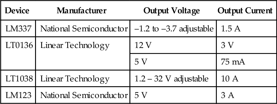
The LM123 is an example of a general purpose linear regulator, providing 5 V at 3 A, and 30 W output power (Linear Technology Corp., 1990). This and equivalent three-terminal regulators having NPN-Darlington pass transistors commonly are found in on-card regulators, laboratory supplies, and instrumentation supplies.
An example of a high-power linear regulator is the LT1038, a three-terminal, bipolar, adjustable voltage regulator capable of providing current in excess of 10 A over the 1.2–32 V range. This high-power device typically is used in battery chargers and system power supplies (Linear Technology Corp., 1990). The output voltage is adjusted by external resistors.
The LT1036 is a logic-controlled dual linear regulator, one providing 12 V at 4 A and the other 5 V at 75 mA. This device is under the control of a logic shutdown signal.
The LM137/LM337 are adjustable negative regulators, delivering up to 1.5 A of output current over an output voltage range of –1.2 V to –37 V. Table 1-3 compares these regulators.
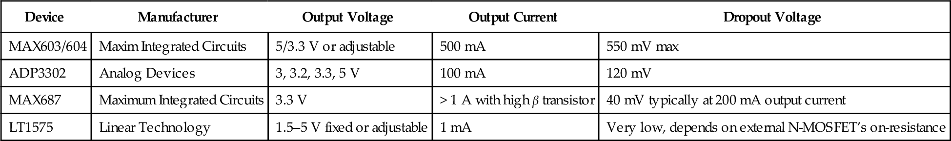
1.3.2.2 Low-Dropout Linear Regulators
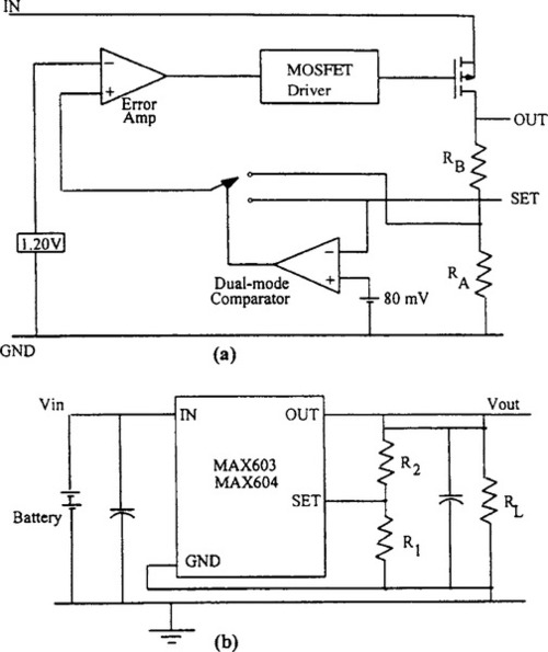
MAX603/604 are dual mode regulators providing either 5 V/3.3 V fixed or adjustable output. Adjustable output from 1.25–11 V may be obtained using external resistors. The P-MOSFET limits quiescent currents to as low as 35 μΑ. This provides several advantages over similar designs using PNP pass transistors, including longer battery life. A functional block diagram of the MAX603/604 is shown in Figure 1-8(a). Its operation as an adjustable reference is shown in Figure 1-8(b) (Maxim Integrated Circuits, 1996). Typical applications of these devices primarily are in battery-powered devices, pagers and cellular phones, and solar-powered instruments.
The ADP330X is a family of precision micro-power low-dropout regulators from Analog Devices. The ADP3302 contains two fully independent regulators. Typical applications of this device are in cellular phones, notebook computers, and portable instruments. MAX687 is a high-accuracy (± 2%) linear regulator controller that directly drives high-gain external PNP transistors. The output current can exceed 1 A with a minimum drive current of 10 mA. It has dropout voltages of 40 mV (at 200 mA output current) and 0.8 V (at 4 A output current).
An LDO controller capable of handling ultrafast current transients is the LT1575 from Linear Technology. This device, along with a discrete N-MOSFET is ideally suited for powering today’s microprocessors such as the Pentium. The nine versions of the LT1575 range from an adjustable-output controller to controllers with fixed outputs of 1.5, 2.8, 3.3, 3.5, and 5 V (Simpson, 1996). Very low-dropout voltages can be obtained, depending on the external MOSFET’s on-resistance.
The UC3833 from Unitrode is described as a linear regulator controller suited for low-dropout, high-current regulators with a high transient response. This device allows the use of a variety of bipolar and MOSFET power devices. The crux of the design lies in the selection of a pass device. The design of a 3.3 V, 4 A regulator suited for today’s microprocessor power supplies is described using this IC with a P-MOSFET in National Semiconductor’s Linear Data Book 1 (1987).
Table 1–4 compares these regulators.
Table 1-4
Low-Dropout Linear Regulators
| Device | Manufacturer | Output Voltage | Output Current | Dropout Voltage |
| MAX603/604 | Maxim Integrated Circuits | 5/3.3 V or adjustable | 500 mA | 550 mV max |
| ADP3302 | Analog Devices | 3, 3.2, 3.3, 5 V | 100 mA | 120 mV |
| MAX687 | Maximum Integrated Circuits | 3.3 V | > 1 A with high β transistor | 40 mV typically at 200 mA output current |
| LT1575 | Linear Technology | 1.5–5 V fixed or adjustable | 1 mA | Very low, depends on external N-MOSFET’s on-resistance |
1.4 Switching Regulators
1.4.1 Switching Regulator Fundamentals
Although the linear regulator is a mature technology, due to its low efficiency and other associated disadvantages, this type of power supply tends to be unfit for most of today’s compact electronic systems.
The disadvantages of the linear regulator are greatly reduced by the switching regulator. In this technology, the AC line voltage is directly rectified and filtered to produce a raw high-voltage DC. This in turn is fed into a switching element that operates at a high frequency, 20 kHz to 1 MHz, chopping the DC voltage into a square wave. The square wave then is filtered to produce a DC output. The input/output relationship of this DC/DC converter is directly related to the duty cycle of the chopping signal. Regulation is achieved by sampling the output, comparing it with a reference, and modifying the duty cycle of the chopping waveform to compensate for any drifts.
Today, most switchers operate well above 500 kHz, with new magnetics, resonant techniques, and surface mount technology extending this to several MHz. Therefore, the associated components such as transformers and capacitors are much smaller than for linear regulators. In addition, due to the lower power loss, smaller heat sinks may be used. Therefore, the overall size of a switching regulator is smaller than an equivalent linear regulator.
The recent rapid advancement of microelectronics has created a necessity for the development of sophisticated, efficient, lightweight power supplies that have a high power-to-volume (W/in3) ratio, with no compromise in performance. High-frequency switching power supplies, able to meet these demands, have become the prime power source in a majority of modern electronic systems. The combination of high efficiency and relatively small magnetics results in compact, lightweight switching regulators, with power densities in excess of 100 W/in3 (Travis, 1996; Goodenough, 1995b) versus 0.3 W/in3 for linear regulators.
However, a major design concern in such high-frequency switching power supplies is minimization of the EMI pollution generated.
1.4.1.1 Modes of Operation
The DC to DC converter has two major operational modes for switching power supplies: the forward mode and the flyback mode. Although they have only subtle differences between them with respect to component arrangement, their operation is significantly different and each has advantages in certain areas of application.
Forward Mode Converters
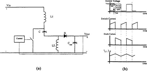
Figure 1-9(a) shows a simple forward mode converter. This type of converter can be recognized by an L-C filter section, directly after the power switch (a power transistor or power MOFSET operating between fully conducting and cutoff modes) or after the output rectifier on the secondary of a transformer.
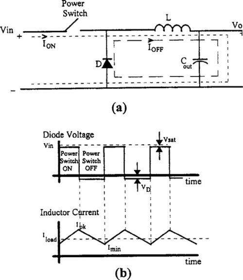
The operation of the converter can be seen by breaking its operation into two periods:
• Power switch on period When the power switch is on, the input voltage is presented to the input of the L-C section and the inductor current ramps upward linearly. During this period the inductor stores energy.
• Power switch off period. When the power switch is off, the voltage at the input of the inductor flies below ground since the inductor current cannot change instantly. Then the diode becomes forward biased. This continues to conduct the current that was formally flowing through the power switch. During this period, the energy that was stored in the inductor is dumped onto the load. The current waveform through the inductor during this period is a negative linear ramp. The voltage and current waveforms for this converter are shown in Figure 1-9(b). The DC output load current value falls between the minimum and the maximum current values and is controlled by the duty cycle. In typical applications, the peak inductor current is about 150% of the load current and the minimum is about 50%.
The advantages of forward mode converters are that they exhibit lower output peak-to-peak ripple voltages and they can provide high levels of output power, up to kilowatts.
Flyback Mode Converters
In this mode of operation, the inductor is placed between the input source and the power switch, as shown in Figure 1-10. This circuit also is examined in two stages:
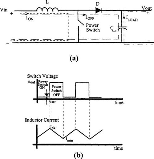
• Power switch on period. During this period, a current loop including the inductor, the power switch, and the input source is formed. The inductor current is a positive ramp, and energy is stored in the inductor’s core.
• Power switch off period. When the power switch turns off, the inductor’s voltage flies back the above input voltage, resulting in forward biasing of the diode. The inductor voltage then is clamped at the output voltage. This voltage, which is higher than the input voltage, is called the flyback voltage. The inductor current during this period is a negative ramp.
In Figure 1-10, the inductor current does not reach zero during the flyback period. This type of a flyback converter is said to operate in the continuous mode. The core’s flux is not completely emptied during the flyback period, and a residual amount of energy remains in the core at the end of the cycle. Accordingly, there may be instability problems in this mode. Therefore, the discontinuous mode is the preferred mode of operation for flyback mode converters. The voltage and current waveforms are shown in Figure 1-11.

The only storage for the load in the flyback mode of operation is the output capacitor. This makes the output ripple voltage higher than in forward mode converters. The power output is lower than in forward mode converters, owing to the higher peak currents generated when the inductor voltage flies back. As they consist of the fewest number of components, they are popular in low- to medium-power applications.
1.4.1.2 A Simplified Analysis of DC/DC Converters
The input/output characteristics of all DC/DC converters can be examined by using the requirement that the initial and the final inductor currents within a cycle should be the same for steady-state operation; that is, the net energy storage within one switching cycle in each inductor should be 0. This leads to the volt-second balancefor the inductor, which means that the average voltage per cycle across the inductor must be 0: that is, the volt-second products for the inductor during each switching cycle should sum to 0 (Brown, 1990; Bose, 1992). This can be illustrated using a typical inductor current waveform, as shown in Figure 1-12.
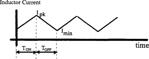
Let the positive slope of the current be m1 and the negative slope m2. For the initial and final currents to be the same,
Since the voltage across an inductor L is given by L di/dt,
Combining (1.5), (1.6), and (1.7),
Equation (1.8) can be written as a function of the duty cycle D:
where VLon and VLoff are the voltages across the inductor during the switch on and switch off periods, respectively, and D is the duty cycle.
The output voltage of forward mode converters is given approximately by Vout ≈ DVin, where D is the duty cycle of the switching waveform. Hence, this mode of operation always performs a step-down operation.
The output voltage for the flyback mode of operation is given by Vout = Vin/(1 – D). Hence, flyback mode converters always are used as step-up converters.
1.4.2 Converter Topologies
The converter topology is the arrangement of components within the converter. Converter topologies fall into two main categories: transformer-isolated and non-transformer-isolated. Each category contains several topologies, with some available in both forms. An excellent discussion on converter topologies is found in Bose (1992).
1.4.2.1 Non-Transformer-Isolated Converter Topologies
This type of switching converter is used when some external component, such as a 50–60 Hz transformer or bulk power supply, provides the DC isolation and protection. These are simple, hence easy to understand and design. However, they are more prone to failure due to the lack of DC isolation. Therefore, these are used by designers mostly in situations such as distributed power systems, where a bulk power supply provides the necessary DC isolation.
There are four basic non-transformer-isolated topologies, the buck (or step down), the boost (or step up), the buck-boost (or inverting), and the Cük converters. Each of these types is described in detail by Linear Technology Corporation (1990, 1992), Datei Inc. (1991), Siliconix Inc. (1994a), Motorola Inc. (1987), and Unitrode Integrated Circuits (1995–96).
1.4.2.2 Transformer-Isolated Converter Topologies
In non-transformer-isolated converter topologies, only semiconductors provide DC isolation from input to output. Transformer-isolated switching converters rely on a physical dielectric barrier to provide galvanic isolation. Not only can this withstand very high voltages before failure, it also provides a second form of protection in the event of a semiconductor failure. Another advantage is the ease of adding multiple outputs to the power supply without separate regulators for each. These features make transformer-isolated topologies preferred by designers.
The transformer-isolated category includes both forward and flyback mode converter topologies. The isolation transformer now provides a step-up or step-down function. The topologies are called isolated, forward, flyback, push-pull, half-bridge, and full-bridge. Each of these types is described in detail by Linear Technology Corp. (1990, 1992), Datel Inc. (1991), Siliconix Inc. (1994a), Motorola Inc. (1987), and Unitrode Integrated Circuits (1995–96).
1.4.2.3 Selection of a Converter Topology
The converter topology has a major bearing on the conditions in which the power supply can operate safely and the amount of power it can deliver. Cost versus performance trade-offs also are needed in selecting a suitable converter topology for an application.
The primary factors that determine the choice of topology are whether DC isolation is needed, the peak currents and voltages to which the power switches are subjected, the voltages applied to transformer primaries, the cost, and the reliability.
Figure 1-13 illustrates the approximate range of usage for these topologies. The boundaries to these areas are determined primarily by the amount of stress the power switches must endure and still provide reliable performance. The boundaries delineated in Figure 1-13 represent approximately 20 A of peak current.
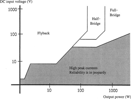
The flyback configuration is used predominantly for low- to medium-output power (150 W) applications because of its simplicity and low cost. Unfortunately, the flyback topology exhibits much higher peak currents than the forward-mode supplies. Therefore, at higher output power, it quickly becomes an unsuitable choice. For medium-power applications (100–400 W) the half-bridge topology becomes the predominant choice. The half-bridge is more complex than the flyback and therefore costs more. However, its peak currents are about one-third to one-half those exhibited by the flyback. Above 400 W, the dominant topology is the full-bridge, which offers the most effective utilization of the full capacity of the input power source. It also is the most expensive to build, but for those power levels, the additional cost becomes a trivial matter. Above 150 W, the push-pull topology sometimes is used. However, this exhibits some shortcomings, such as core imbalance, that may make it tricky to use (Brown, 1994).
Estimating the major power supply parameters at the beginning of the design and using charts such as Figure 1-13 will lead to the selection of a final topology that is safe, reliable, and cost effective.
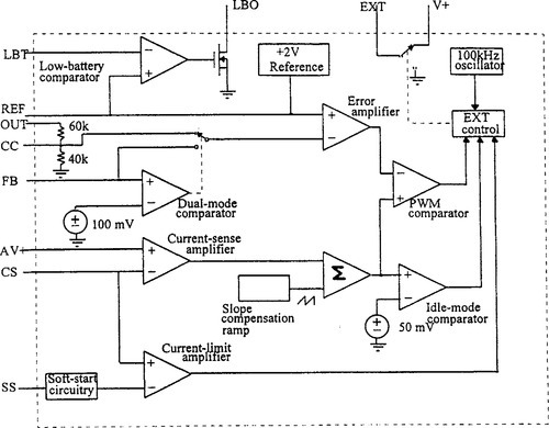
Some relative merits of the converter topologies as well as their advantages, disadvantages, and typical applications are summarized in Table 1-5. Mathematical expressions for estimating some of the important parameters, such as peak currents and voltages and output power, are found in Brown (1990, 1994). A comparison of the strengths and weaknesses of the different converter topologies also is found in Moore (1994).
Table 1-5
Comparison of Converter Topologies
| Topology | Vin/Vout | Advantages | Disadvantages | Typical Application Environment | Vin (dc) Range (V) | Typical Efficiency (%) | Relative Parts Cost |
| Buck | D | High efficiency, simple, low switch stress, low ripple | No isolation, potential overvoltage if switch shorts | Small-sized, Embedded systems | 5–1000 | 78 | 1.0 |
| Boost | 1/(1 – D) | High efficiency, simple, low input ripple current | No isolation, high switch peak current, regulator loop hard to stabilize, high output ripple, unable to control short-circuit current | Power-factor correction, battery up-converters | 5–600 | 80 | 1.0 |
| Buck-Boost | − D/(1 − D) | Voltage inversion without a transformer, simple, high-frequency operation | No isolation, regulator loop hard to stabilize, high output ripple | Inverse output voltages | 5–600 | 80 | 1.0 |
| Flyback | N2D/N1 (1 – D) | Isolation, low parts count, has no secondary output inductors | Poor transformer utilization, high output ripple, fast recovery diode required | Low output power, multiple output | 5–500 | 80 | 1.2 |
| Push-Pull | 2 N2D/N1 | Isolation, good transformer utilization, good at low input voltages, low output ripple | Cross-conduction of switches possible, high parts count, transformer design critical, high voltage required for switches | Low output voltage | 50–1000 | 75 | 2.0 |
| Half-bridge | N2D/N1 | Isolation, good transformer utilization, switches rated at input voltage, low output ripple | Poor transient response, high parts count, cross-conduction of switches possible | High input voltage, moderate to high power | 50–1000 | 75 | 2.2 |
| Full-bridge | 2N2D/N1 | Isolation, good transformer utilization, switches rated at input voltage, low output ripple | High parts count, cross-conduction of switches possible | High power, high input voltage | 50–1000 | 73 | 2.5 |
The industry has settled into several primary topologies for a majority of the applications. Due to reasons discussed before, transformer-isolated topologies have become more popular than non-transformer-isolated topologies.
1.4.3 Control Techniques
Two basic methods of control are used in switching regulators: pulse width modulation (PWM) and resonant. In both techniques, the output voltage is sampled and the switching of the transistors is modified in some manner to keep the output constant.
1.4.3.1 Pulse Width Modulation Control Techniques
In a PWM switch mode power supply, a square wave pulse normally is generated by the control circuit to drive the switching transistor on and off. By varying the width of the pulse, the conduction time of the transistor correspondingly is varied, regulating the output voltage. The major function of the control subsection of a PWM supply therefore is to sense any change in the DC output voltage and adjust the duty cycle of the power switches to correct for such changes.
An oscillator sets the basic frequency of operation of the power supply. A stable, temperature-compensated reference is used, to which the output voltage is compared in a high-gain voltage error amplifier. An error voltage-to-pulse width converter is used to adjust the duty cycle.
The PWM control circuit may be single ended for driving single-transistor converters, such as the buck or boost topology, or it may be double ended to drive multiple-transistor converters, such as the push-pull or half-bridge topology.
Two basic modes of control are used in PWM converters: voltage mode and current mode.
Voltage-Mode Control
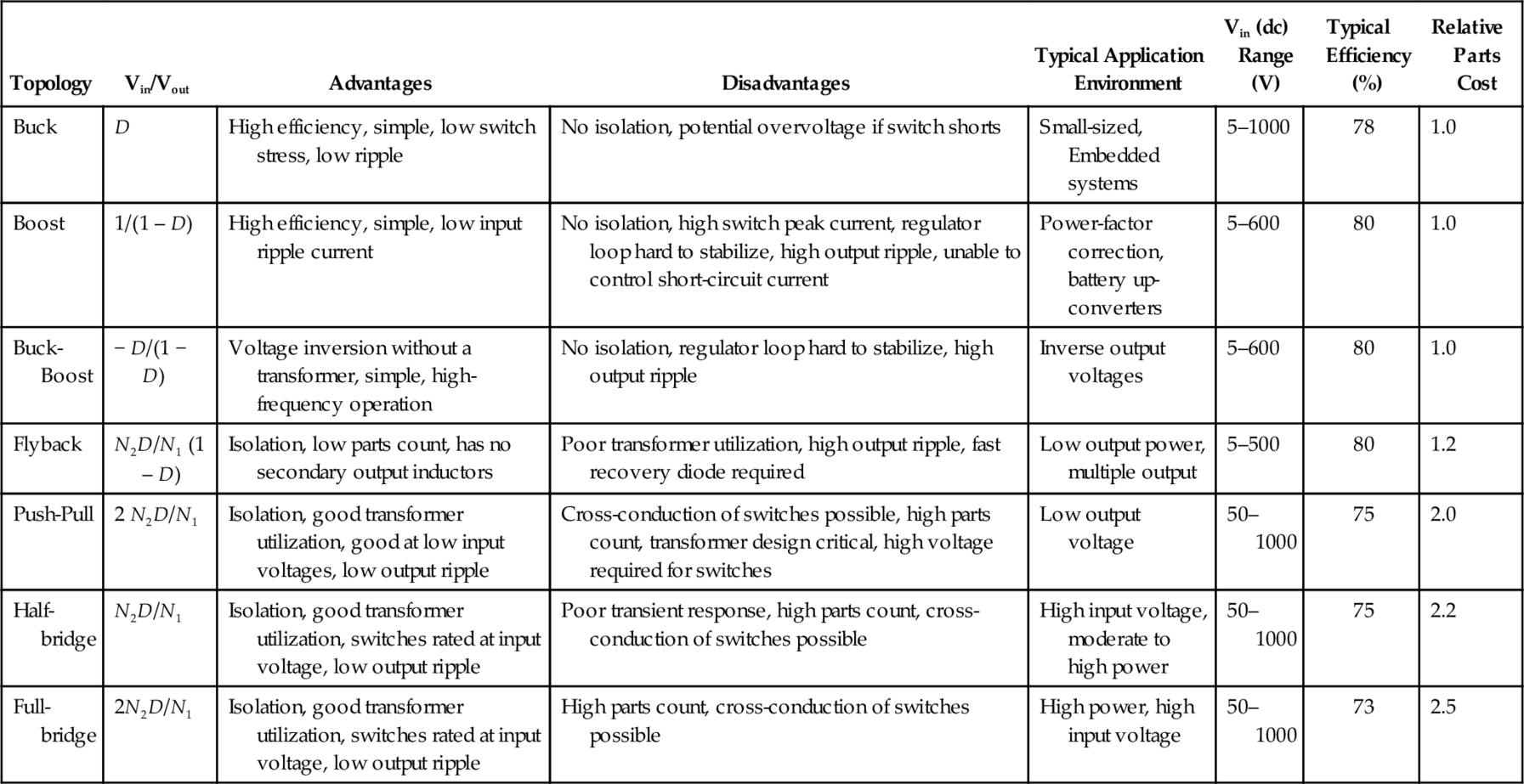
This is the traditional mode of control in PWM switching converters. It also is called single-loop control, as only the output is sensed and used in the control circuit. A simplified diagram of a voltage-mode control circuit is shown in Figure 1-14.
The main components of this circuit are an oscillator, an error amplifier, and a comparator. The output voltage is sensed and compared to a reference. The error voltage is amplified in a high-gain amplifier. This is followed by a comparator, which compares the amplified error signal with a sawtooth waveform generated across a timing capacitor.
The comparator output is a pulse width modulated signal that corrects any drift in the output voltage. As the error signal increases in the positive direction, the duty cycle is decreased; and as the error signal increases in the negative direction, the duty cycle is increased.
The voltage mode control technique works well when the loads are constant. If the load or the input changes quickly, the delayed response of the output poses a drawback to the control circuit, as it senses only the output voltage. Also, the control circuit cannot protect against instantaneous overcurrent conditions on the power switch. These drawbacks are overcome in current mode control.
Figure 1-15 shows a functional block diagram of the commonly used TL494 voltage mode controller. Control for both push-pull and single-ended operation can be achieved with this chip. The frequency of the oscillator is set by the external resistors RT and CT. The typical operating frequency is 40 kHz, and the maximum is 200 kHz.

Output pulse width modulation is accomplished by comparison of the positive sawtooth waveform across the capacitor to either of two control signals. The NOR gates, which drive the output transistors, are enabled only when the flip-flop clock input is in its low state. This happens only during that portion of time when the sawtooth voltage is greater than the control signals. Therefore, an increase in control signal amplitude causes a corresponding linear decrease of output pulse width.
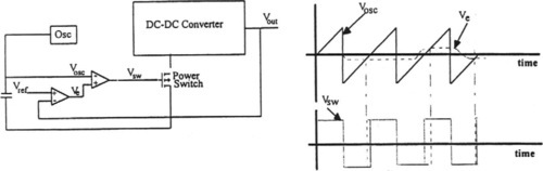
Current-Mode Control
This is a multiloop control technique, which has an AC current feedback loop in addition to the voltage feedback loop. The second loop directly controls the peak inductor current with the error signal rather than controlling the duty cycle of the switching waveform. Figure 1-16 shows a block diagram of a basic current mode control circuit.
The error amplifier compares the output to a fixed reference. The resulting error signal then is compared with a feedback signal representing the switch current in the current sense comparator. This comparator output resets a flipflop that is set by the oscillator. Therefore, switch conduction is initiated by the oscillator and terminated when the peak inductor current reaches the threshold level established by the error amplifier output. Thus, the error signal controls the peak inductor current on a cycle-by-cycle basis. The level of the error voltage dictates the maximum level of peak switch current. If the load increases, the voltage error amplifier allows higher peak currents. The inductor current is sensed through a ground-referenced sense resistor in series with the switch.
The disadvantages of this mode of control are loop instability above 50% duty cycle, less than ideal loop response due to peak instead of average current sensing, and a tendency toward subharmonic oscillation and noise sensitivity, particularly at very small ripple current.
However, with careful design as explained by Brown (1990), Cryssis (1989), and others, these disadvantages can be overcome. Therefore, current-mode control becomes an attractive option for high-frequency switching power supplies.
Figure 1–17 shows a functional block diagram of the MAX747 current mode controller from Maxim Integrated Circuits (1994). This is a CMOS step-down controller, which drives external P-channel FETs. The IC operates in a continuous mode under heavy loads but in a discontinuous mode at light loads stability of the inner current-feedback loop is provided by a slope-compensation scheme that adds a ramp signal to the current-sense amplifier output. The switching frequency nominally is 100 kHz and the duty cycle varies from 5 to 96%, depending on the input/output voltage ratio. EXT provides the gate drive for the external FET.
1.4.3.2 Resonant Control Techniques
The term resonance refers to a continuous sinusoidal signal. Resonant converters process power in a sinusoidal form. Resonant techniques have long been used with thyristor converters, in high-power SCR motor drives, and in UPSs. However, due to its circuit complexity, it had not found application in low-power DC-to-DC converters until recently. With the development of surface mount technology, resonant forms of DC-to-DC converters have gained rapid acceptance recently, harnessing certain advantages inherent in resonant techniques. The thrust toward resonant mode power supplies has been fueled by the industry’s demand for miniaturization, together with increasing power densities and overall efficiency, and low EMI.
With available bipolar devices and circuit technologies, PWM converters have been designed to operate with switching frequencies in the range 50–200 kHz. The advent of power MOSFETs enabled the switching frequencies to be increased to several MHz. However, increasing the switching frequency, although allowing for miniaturization, leads to increasing switching stresses and losses, which leads to a reduction in efficiency. The detrimental effects of the parasitic elements also become more pronounced as the switching frequency is increased. With quasi-resonant techniques, higher frequency as well as higher efficiency compared to PWM techniques are achieved.
Resonant circuits in power supplies operate in two modes that define the flow of current in the resonant circuit: continuous and discontinuous. In the continuous mode, the circuit operates either above or below resonance. The controller shifts the frequency either toward or away from resonance, using the slope of the resonant circuit’s impedance curve to vary the output voltage. This is a truly resonant technique but is not commonly used in power supplies due to its high peak currents and voltages.
In the discontinuous mode, the control circuit generates pulses having a fixed on-time but at a varying frequency, determined by the load requirements. This mode of operation does not generate continuous current flow in the tuned circuit, is the common mode of operation in a majority of resonant converters, and is called the quasi-resonant mode of operation.
The Quasi-Resonant Principle
The quasi-resonant principle is used in power converters by incorporating a resonant LC circuit with the power switch. The power switch is turned on and off in the same manner as in PWM converters, but the tank circuit forces the current through the switch into a sinusoidal form. The actual conduction period of the switch is governed by the resonant frequency fr of the tank circuit. This basic principle is illustrated in Figure 1-18.
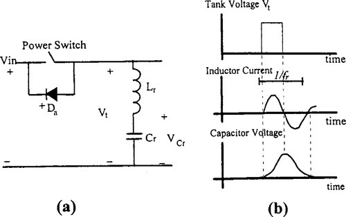
The tank circuit exhibits a relatively fixed ringing period to which the conduction period of the power switch is slaved.
The on-period of the power switch is fixed to the resonance period of the tank elements. The quasi-resonant supply is controlled by changing the number of on-times of the power switch per second.
All resonant control circuits keep the pulse width constant and vary the frequency, whereas all PWM control circuits keep the frequency constant and vary the pulse width. The main advantages of the quasi-resonance techniques arise from the sinusoidal wave shapes of the switching currents and voltages. The switching losses are reduced, leading to higher efficiency and greatly reduced EMI.
The resonant switch consists of a semiconductor switch and resonant LC elements. Because resonant circuits generate sinusoidal waves, designers can operate the power switches either at zero current or at zero voltage points in the resonant waveform. Based on this, there are two types of resonant switches: zero current switches (ZCS) and zero voltage switches (ZVS). The two types of switches are the duals of each other. A description of the operations of these switches is found in Brown (1990).
Comparable converter topologies as with the PWM technique are available with ZCS and ZVS quasi-resonant switching techniques. Circuits for each of these topologies are found in Brown (1990, 1994), Cük and Middlebrook (1994), Steigerwald (1984), and Cük and Maksimovic (1988).
Control Techniques
Control methods for resonant converters are variable frequency ones. Either the on-time is fixed and the off-time is variable or vice versa.
The basic functioning of a resonant mode control circuit is shown in Figure 1-19. The fundamental blocks are a wide-band error amplifier, a voltage-controlled oscillator (VCO), and a temperature-stable one-shot timer.
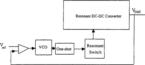
The output voltage is compared with the reference, and the error voltage is used to drive the VCO. The VCO output triggers the one-shot timer, whose pulse duration is fixed as required by the converter. These control techniques are based on the voltage mode of control and, hence, suffer from poor input transient response characteristics.
Some representative control ICs currently available are the MC34066, LD405, UC1860, and UC3860. One of the first resonant mode controller ICs to appear on the market was the LD405. Subsequently, the CS3805 by Cherry Semiconductors and an improved GP605 by Gennum Corp. were released.
The LD405 and the CS3805 have drive current capabilities of 200 mA and operating frequencies in the range 10 kHz–1 MHz. They have single-ended and complementary outputs for driving power MOSFETs. The dissipation rate is specified at 500 mW at 50°C. The operating range of the GP605 is between 1 kHz and 1.2 MHz.
Unitrode Integrated Circuits introduced its UC3860 family of resonant mode controller chips in 1988. These could supply 800 mA, about four times the drive current, and operate at higher frequencies (up to 2 MHz) than the previously available ICs. Their power dissipation rate is specified at 1.25 W at 50°C.
A newer series of resonant mode control chips by Unitrode Integrated Circuits and their applications are described in Wofford (1990). These are the UC3860, UC1861 (dual ZVS), UC1864 (single ZVS), and UC1865 (dual ZCS).
A functional block diagram of the UC1860 from Unitrode Integrated Circuits (1995–96) is shown in Figure 1-20. The nominal operating frequency for this IC is 1.5 MHz, and the device implements resonant mode, fixed on-time control as well as a number of other power supply control schemes with its various dedicated and programmable features. The IC contains dual high-current totempole output drivers that can be programmed to operate alternately or in unison (Unitrode Integrated Circuits, 1995–96).
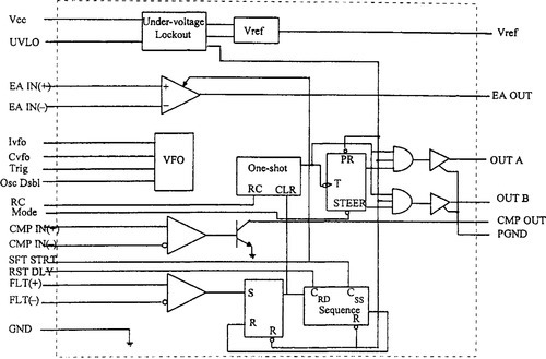
Although varying in detail and complexity, all these resonant mode control chips provide the same basic functions. All contain a VCO that varies the operating frequency, a monostable circuit that establishes the pulse on-time, and a steering circuit that determines the output drive mode (controlled on- or off- times, single-ended, or complementary). The chips also provide many of the same basic protection features such as soft start, undervoltage lockout, and overload protection — although in different ways and with varying degrees of sophistication. Some of these control ICs are also described by Linear Technology Corporation (1990, 1992), Datel Inc. (1991), Siliconix Inc. (1994a), Motorola Inc. (1987), and Unitrode Integrated Circuits (1995–96).
1.4.4 Special Application Requirements
1.4.4.1 Sub-5 V Applications
As IC process lithography becomes finer and the need to reduce overall power dissipation becomes more important, ICs demand lower and better-regulated power supply rails. Power supply rails for modern microprocessors and logic ICs have dropped below 5 V to a 3.3 V pseudo-standard and are fast heading toward sub-2 V and sub-1 V levels.
These low-voltage supply requirements also differ in voltage level from system to system and from version to version of the same IC. If Intel’s Pentium processor is taken as an example, some versions just require 3.3 V while others require two supplies at 3.3 V and 3 V. Yet other versions require supplies such as 3.383 V and 3.525 V, being the optimum voltages for maximum speed in the respective versions. Furthermore, the Pentium Pro comes with a 4-bit operating voltage code, which selects 1 of 16 discrete voltages between 2 and 3.5 V (Travis, 1996; Goodenough, 1995b, 1995c, 1996).
Lower voltage levels, however, do not translate to low power. These multimillion-transistor ICs use CMOS technology, which at today’s high operating frequencies consume substantial amounts of current although virtually no DC current. The power levels required therefore are rising. Top-of-the-line CPU power is approaching 100 W; and desktop CPU, power 30 W. Systems such as high-performance multiprocessor servers are approaching 400–600 W. The combination of increasing power requirements and reducing voltage rails requires the power source to provide and distribute very high currents within a system. For example, a 300 W system running off a 3 V supply must provide and distribute 100 A of current.
Furthermore, clock rates heading toward 400–600 MHz imply high current transients as devices come out of the sleep mode within a clock cycle of a few nanoseconds.
In addition to microprocessors, high-speed data buses, such as the 60 MHz GTL (Gunning Transceiver Logic) bus, are being recommended for interconnection of processors and peripherals on the motherboard. These require an active 1.2 or 1.5 V terminator at each end, each potentially capable of handling up to 7 A. Other data buses with similar requirements include Futurebus (2.1 V) and Rambus (2.7 V) (Goodenough, 1995c). Therefore, the challenges facing the power supply designer in the sub-5 V range can be summarized as follows:
• Tight tolerances.
• High efficiency while generating high current (low power loss).
• High accuracy.
• High current transients.
The basic design requirements in the face of these challenges are low power loss and higher gain and bandwidth in the control loop to handle tighter voltage regulation and transients.
1.4.4.2 Converters for Battery-Operated Equipment and Battery Chargers
The proliferation of portable computers and handheld communication devices has opened up another branch in DC/DC converter evolution. Users of these portable devices demand features such as compactness, lightness, and low power consumption for extended periods of operation. Corresponding trends in DC/DC converters emphasize excellent conversion efficiency and compactness.
Additional constraints placed on the DC/DC converter include minimum noise intrusion into communication and audio circuits in the device. The increase in the integration of high-speed modems and CD-ROM drives into portable computers has made power supply switching noise an important consideration.
A key requirement for designers of battery-powered products is that they minimize the number of cells used in the product. Products ideally should run off a few high-capacity cells to minimize size and cost. Tiny devices such as pagers run off one or, at most, two cells. So do telephones and PDAs. Converters operating off input sources as low as that of a single-cell alkaline battery (1 V) are needed. Therefore, the voltage required, in most instances, is greater than the voltage available from the cells. Furthermore, for extended battery life, the converter should be able to operate from waning batteries.
Some systems need to operate with input voltages that approach the output voltage. This low-dropout condition requires the DC/DC converter duty cycle to approach 100%. Furthermore, a waning battery may swing the input voltage from a value above the output to one below it.
High efficiency is another prime consideration in battery-operated equipment. This means not only increased operating time on a battery charge but also reduced heat that must be dissipated in or removed from the IC and the device. Low quiescent current is another requirement for extended battery charge.
Therefore, the challenges facing the power supply designer for battery-powered equipment can be summarized as follows:
• Extended use of battery charge.
• Small size.
• Low EMI.
1.4.5 Practical Design Approaches
This section describes-some of the approaches taken in DC/DC converter and controller design to address the special requirements of sub-5 V and battery-powered applications. Illustrative examples of some successful solutions are presented.
1.4.5.1 Synchronous Rectification
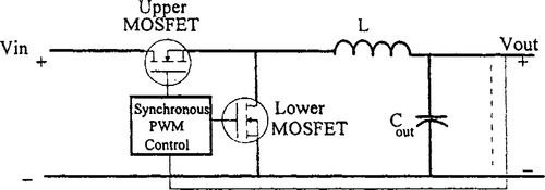
In a conventional DC/DC converter such as the buck converter, typically an N-channel MOSFET with a low RDS(on) is selected for the switch. However, the diode’s forward voltage becomes a limiting factor in improving the converter’s efficiency, as the output voltage drops. This has led to the design of synchronous converters; these replace the diode, which normally is a Schottky, with another N-channel MOSFET. This usually is called the lower MOSFET, and the switch is called the upper MOSFET. The lower MOSFET conducts current during the off-time of the upper MOSFET. Figure 1-21 shows a simplified diagram of a synchronous buck converter. In conventional synchronous converters, a single IC is used for PWM control and the synchronous drive of two external MOSFETs.
Newer process technologies take another approach, where a SynchroFET integrates the two MOSFETs, their drive circuits, and the synchronous control logic. This IC can be used with a conventional PWM control IC to design a converter with features superior to those with discrete MOSFETs (Maxim Integrated Circuits, 1997). Also, this approach allows the SynchroFET to be paired with many different PWM controllers to achieve various performance trade-offs.
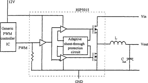
HIP5015 and HIP5016 are a widely used pair of SynchroFETs from Harris Semiconductor. A 5 V to 3.3 V DC/DC converter using a generic PWM controller and the HIP5015 SynchroFET is shown in Figure 1-22. This typically is used to derive 3.3 V from a 5 V input. The implementation of a two-output converter using these SynchroFET ICs is described in Goodenough (1996). The HIP5015/5016 is designed to run at over 1 MHz. The efficiency of a 5 to 3.3 V converter running at 400 kHz using this IC is reported to be 85% for load currents between 0.5 and 4.5 A and over 90% for load currents between 0.8 and 2.8 A (Goodenough, 1996). The newer HIP5020 synchronous buck converter (Harris Corp., 1997) is optimized for battery-powered systems with 4.5–18 V input. This buck converter can be operated up to a switching frequency of 1 MHz and demonstrates an efficiency of over 95%.
1.4.5.2 Increased Gain and Bandwidth Control Loop
In low-voltage synchronous converters, the preferred method of control is the voltage mode. The power dissipated in the current sense resistor in current mode control cuts the efficiency by about 2% and therefore is unsuitable for low-voltage, high-efficiency applications. However, the low bandwidth of the voltage mode control loop reduces the converter’s response to dynamic load conditions.
Maxim’s three PWM controllers, the MAX796/797/799 designed for portable computer and communication applications, are current mode controllers that drive synchronous rectifiers, primarily in the buck mode. Efficiencies as high as 97% are reported by Maxim Integrated Circuits (1997).
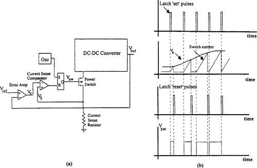
Figure 1-23 shows the MAX797 controller. The special features of this circuit are a proprietary PWM comparator for handling transients, a proprietary idle mode control scheme used at low-load conditions for extended battery life, and the reduction of PWM noise.
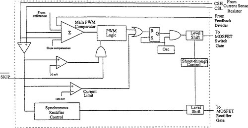
This series is designed for output voltages as low as 2.5 V but can provide 1.5 V with external circuitry. To provide the required DC accuracy at the low-output voltage while handling high-speed current transients, these devices require an external op amp in the error amplifier circuit, which operates as an integrator (Maxim Integrated Circuits, 1997).
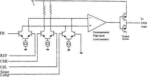
The heart of this PWM controller is a multi-input open-loop comparator that sums the output voltage error with respect to the reference, the current sense signal, and a slope compensation ramp. This is of the direct summing type and lacks the traditional error amplifier with the associated phase shift. This direct summing configuration approaches the ideal of direct cycle-by-cycle control of the output voltage. This PWM comparator is shown in Figure 1-24.
1.4.5.3 Idle Mode Control Scheme
The MAX797’s approach for conservation of battery power uses the SKIP input shown in Figure 1-23. At light loads (SKIP = 0) the inductor current fails to exceed the 30 mV threshold set by the minimum current comparator. When this occurs, the minimum current comparator immediately resets the high-side latch at the beginning of the cycle unless the output voltage drops below the reference. This sends the controller into a variable-frequency idle mode, skipping most of the oscillator pulses, to cut back on gate-charge losses.
Operation at a fixed frequency, regardless of load conditions, however, is advantageous in terms of lowering PWM noise interference. Steps can be taken to remove the known emissions at fixed frequencies. Therefore, a low-noise mode is enabled in the MAX797 by making SKIP high. This forces fixed frequency operation by disabling the minimum current comparator.
1.4.5.4 Updated Voltage Mode Control
A newer solution by Linear Technology employs an advanced voltage mode control scheme in its LTC1430 controller. This controller, optimized for highpower, 5 V/3.x V applications, operates at an efficiency greater than 90% in converter designs from 1 A to greater than 50 A output current (Linear Technology Corp., 1995). The LTC1430 uses a synchronous switching architecture with two N-channel output devices.
A block diagram of the LTC1430 is shown in Figure 1-25. The primary control loop is a conventional voltage mode feedback loop. The load voltage is sensed across the output capacitor by the SENSE + and SENSE– inputs, divided and fed to the feedback amplifier, where it is compared to a 1.26 V interval reference. The error signal then is compared to a sawtooth waveform from the oscillator to generate a pulse width modulated switching waveform.
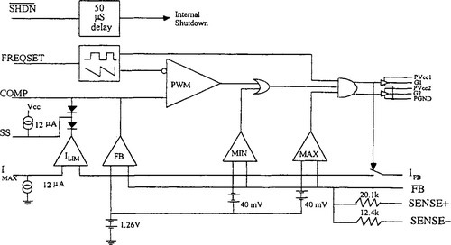
Two other comparators in the feedback loop, MIN and MAX, provide high-speed fault correction in situations where the feedback amplifier may not respond quickly enough. MIN compares the feedback signal to a voltage 40 mV (3%) below the reference, and MAX compares it to a voltage 3% above the reference. If the output falls below the minimum level, the MIN comparator overrides the feedback comparator and forces the loop to full duty cycle (about 90%). If the output rises above the 3% level, the MAX comparator forces the duty cycle to 0. These two comparators prevent extreme output perturbations in the presence of fast output transients.
Additionally, the controller senses output current across the drain source resistance of the upper N-channel FET, providing an adjustable current limit without an external sense resistor.
1.4.5.5 A Master/Slave Architecture
Power Trends’ solution (Travis, 1996) is a master/slave architecture for DC/DC converter modules, which allows the increase of available current in 3 A steps. This design consists of a 5 V/3.3 V converter with a 3 or 8 A master coupled with three 3 A slaves. The slaves add 9 A of current to the master’s current output. This approach is an attractive solution, which leaves room for future system upgrades.
1.4.5.6 Improved Process Technologies
Aiming at improved control loop bandwidth, Siliconix developed a highspeed CBiC/D (complementary bipolar/CMOS/DMOS) process that provides vertical PNP transistors with an f t of 2 GHz. The Si9145 voltage mode controller built with this technology has an error amplifier with a functional closed-loop bandwidth of 100 kHz, helping to handle transient loads provided by today’s microprocessors (Goodenough, 1995c).
1.4.5.7 Switched Capacitor Converters
Switched capacitor (charge pump) converters use capacitors rather than inductors or transformers to store and transfer energy. The most compelling advantage of these converters is the absence of inductors. Compared with capacitors, inductors have greater component size, more EMI, greater layout sensitivity, and higher cost.
Compared with other types of voltage converters, the switched capacitor converter can provide superior performance in applications that process low-level signals or require low-noise operation.
Many capacitor-based voltage converters offer extremely low operating current, a useful feature in systems for which the load current is either uniformly low or low most of the time. Thus, for small handheld products, the light-load operating currents can be much more important than full-load efficiency in determining battery life (Williams and Huffman, 1988). The basic operation of switched capacitor voltage converters is shown in Figure 1-26.
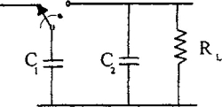
When the switch is in the left position, C1 charges to V1. The total charge on C1 is given by q1 = C1V1. When the switch moves to the right position, C1 discharges to V2. The total charge on C1 now is given by, q2= C1V2. The total charge transfer is given by
If the switch is cycled at a frequency f, the charge transfer per second (the current) is given by
Where Req is given by 1/f C1 The reservoir capacitor C2 holds the output constant. The basic charge pump circuit can be modified for an inverted output by flipping C1 in the internal switching arrangement. It can be used for doubling, tripling, or halving the input voltage with different external connections and by the use of external diodes.
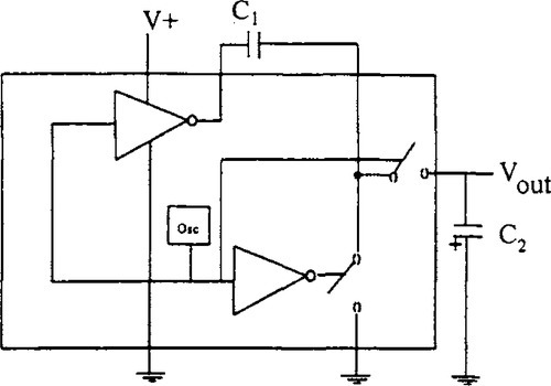
Figure 1-27 shows a simple switched capacitor IC implementation with on-chip switches. The usage of switched capacitor converters in laptop computers and small handheld communication devices is increasing as their output current capabilities are increasing and the supply current required by the portable devices is decreasing.
Simple switched capacitor converters such as the MAX660 can generate 100 mA at 3.3 V when powered from a two-cell battery of alkaline, NiCd, or NiMH cells or a single primary lithium cell. A disadvantage of a circuit such as this is the lack of regulation, which is overcome by adding a regulator externally.
Internal regulation in monolithic switched capacitor converter chips is achieved either as linear regulation or as charge pump modulation. Linear regulation offers low output noise. Charge pump modulation controls the switch resistance and offers more output current for a given cost or size because of the absence of a series-pass resistor. Newer charge pump ICs employ an on-demand switching technique that enables low quiescent current and high output current capability at the same time.
The simplicity of switched capacitor circuits, and hence its suitability for miniature equipment, is amply illustrated by Siliconix Inc. (1994b), where the eight-pin Si7660 is used for voltage inversion, doubling, and splitting.
1.4.5.8 SEPIC
The SEPIC (single-ended primary inductance converter) architecture is especially suited for battery-operated equipment and battery charger applications. The SEPIC topology is shown in Figure 1-28.
The two inductors L1 and L2 often are two identical windings on the same core. This topology essentially is similar to a 1:1 transformer flyback converter, except for the addition of a capacitor C, which forces identical AC voltages across the two inductors. This is a step-up/step-down topology with no inversion and no transformer. However, the SEPIC topology provides DC isolation from the input to the output through the presence of the capacitor.
The input/output relationship for this converter is given by
This topology has the advantage of being operable over a wide input voltage range. Due to this, the topology commonly finds applications in battery-powered equipment and battery chargers.
A converter design using the LT1373 current mode switching regulator with a SEPIC converter for generating 3.3 V from a single lithium-ion battery is described in Essaff (1995). In a typical application such as this, the battery voltage at full charge is above the output voltage; and when discharged, it is below the output voltage. This presents special difficulties in the converter design. The SEPIC architecture, with its wide input voltage range, is ideally suited for such applications.
The use of the SEPIC topology in battery charging is illustrated in an application by Linear Technology Corp. (1996). The topology allows charging even when the input voltage is lower than the battery voltage. Further, it allows the current sense circuit to be ground-referenced and completely separated from the battery itself, simplifying battery switching and system grounding problems.
The LT1512 is a constant current controller for SEPIC converters, for charging NiCd and NiMH batteries. It also can provide a constant voltage source for charging lithium-ion batteries (Linear Technology Corp., 1996). A special feature of this controller is an internal low-dropout regulator, which provides a 2.3 V. supply for all internal circuitry, allowing input voltages to vary from 2.7 to 25 V. This enables charging batteries from varied sources such as wall adapters, car batteries, and solar cells.
1.4.6 Illustrative DC to DC Converter ICs and Applications
The modularity of design, the wide-ranging power supply requirements, and the need for compactness, portability, and expandability of today’s electronic equipment all contribute to the numerous applications that DC/DC converters have found in modern electronic equipment.
The area in which DC/DC converters have found the widest application is in distributed power systems. A distributed power system uses many small regulated power supplies, each located as close as possible to the load (Goodenough, 1995a). The bulk supply develops and distributes via a bus, an arbitrary voltage level. At appropriate points DC/DC converters change this voltage to the levels needed for the local circuitry. A distributed power system can save space and reduce the weight of the system. It also can improve reliability and the quality of the generated power and facilitate modular design and system expansion. Issues relating to distributed power systems are discussed in Ormond (1990, 1992) and Goodenough (1995a).
A typical application of a distributed power system is in telecommunication equipment. A relatively high-voltage battery of 48 V is located in the bottom of each electronic equipment rack and DC/DC converters are used on each rack card cage to step down the voltage to the required level. Another such application is in aircraft power distribution systems.
Modern electronic systems contain both analog and digital circuitry, where analog components require voltage levels such as 9, ± 12, and ± 15. In mixed mode logic circuits, the conventional 5 V supply and a 3.3 V supply for the latest low-power ICs are required. In such complex cases, DC/DC converters perform the valuable function of generating all required voltages while saving cost and space. A common application of 5–12 V converters is in flash memory programmers, which require a supply of 12 V.
Battery chargers that can be used off diverse power supplies, ranging from the conventional main supply to solar cells, find the step-up/step-down ability of DC/DC converters a useful feature.
Another application area of DC/DC converters is in small, battery-operated, portable equipment such as pagers, cameras, cellular phones, laptop computers, remote data acquisition, and instrumentation systems. The high efficiency and the small size of DC/DC converters become especially useful in such applications.
1.4.6.1 DC/DC Converter ICs
An increasing variety of chip-level DC/DC converters are appearing on the market. These devices not only are changing the way system designers structure their power supplies but are providing solutions to applications that previously required more costly, bulky, and cumbersome approaches.
Integrated circuit DC/DC converters are available in a wide range of power and other capabilities. The lower-power ICs can supply the exact voltage needed for a specific IC board, and higher-power types can simplify the design by reducing the component count (Pryce, 1988).
The key parameters and capabilities of modern low-power DC/DC converters are described in this section using a representative sample from principal manufacturers such as Maxim Integrated Circuits, Datel Inc., Linear Technology Corp., and Harris Semiconductor. For example, output power capabilities range from less than 1 W to more than 300 W. Single, double, or triple output configurations are available. Common output voltages are 3.3, 5, 12, and 15 V, while input voltages are quite varied. Common devices perform 5 to 12 V, 9 to 12 V, and 5 to 3.3 V conversions. Table 1-6 shows key features of some representative DC/DC converters.
Table 1-6
Some Representative DC/DC Converter ICs
| Manufacturer | Model | Output power (W)/Output Current (A) | Output Voltage (V) | Input Voltage (V) |
| Linear Technology Crop. | LT1070 | 5 A | Circuit dependent | 3 to 6 |
| LT1073 | 0.5 W | 5, 12 | 1 to 12 | |
| LT1074/76 | 5/2 A | 5 | 7 to 45/64 | |
| LT1173 | 0.5 W | 5, 12 | 2 to 12 (step down) | |
| 2 to 30 (step up) | ||||
| Datel Inc. | XWR series | 3, 10, 20 W | 3.3, ± 5, ± 12, ± 15 | 4.6 to 13.2, 4.7 to 7, 9 to 18, 18 to 72 |
| Maxim Integrated | MAX632 | 0.025 A | 12 | 2 to 12.6 |
| Circuits | MAX742 | 1 A | 5, 12, 15, 28 | 2 to 16.5 |
| MAX756 | 0.3 A | 3.3, 5 | 1.1 to 5.5 | |
| Siliconix Inc. | Si9100 | 0.350 A | Vout < Vin | 10 to 70 |
| Si9102 | 0.250 A | Vout < Vin | 10 to 120 | |
| Si7660 | Up to 100 mA depending on Vin/Vout | − Vin, 2Vin, Vin/2 | 1.5 to 10 | |
| National Semiconductor | LM3578 | 0.750 A | Vout < Vin Vout > Vin | 2 to 40 |
| Harris Crop. | 3.5 A | Vout < Vin | 4.5 to 18 | |
| Analog Devices | ADP3603 | 50 mA | –3 mA | 4.5 to 6 |
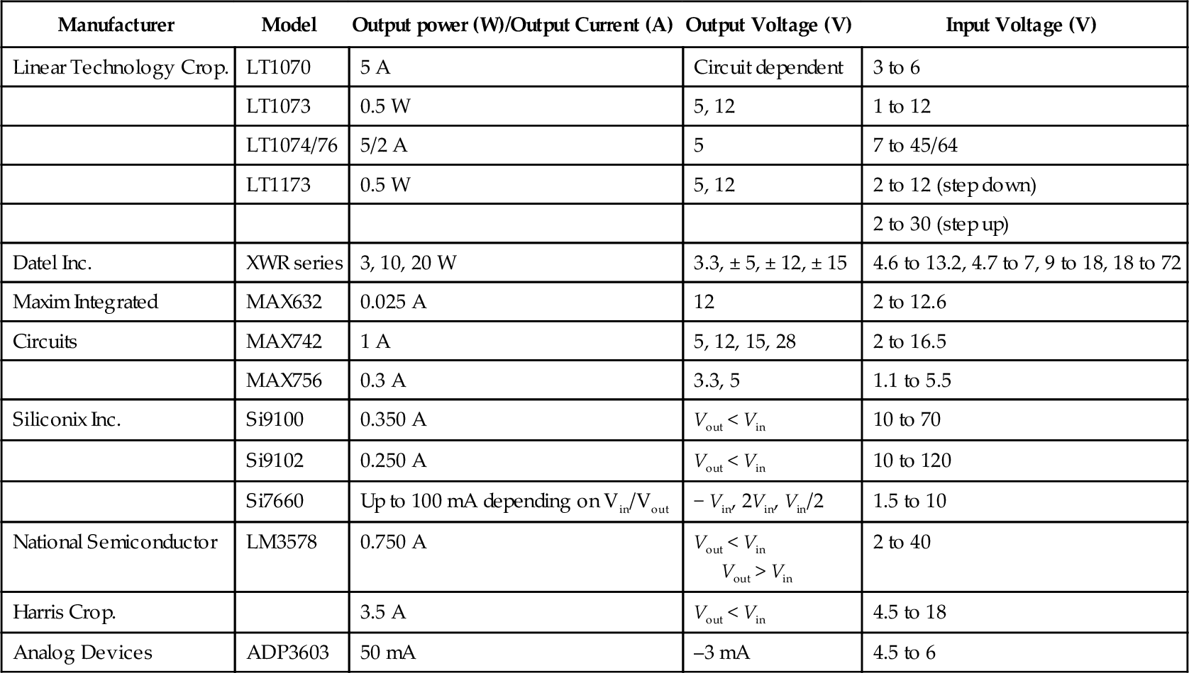
Linear Technology Corp. produces a wide range of DC/DC converters, ranging from 0.5 W micro-power devices to high-efficiency 5 A devices. Simple voltage doublers and dividers as well as circuits that can be used in many configurations are available. The LT1073, a gated oscillator mode IC, can operate from a supply of 1 V and typically is used to generate 5 or 12 V from a single cell.
The XWR (wide input range) series by Datel Inc. (1991) is composed of high-efficiency current mode converters with typical efficiencies of about 85%. Common applications of these are in telecommunication, automotive, avionic, and marine equipment and in portable battery-operated systems. In addition to the XWR series, Datei also has the LP series of converters having 3, 4.5, 5, and 10 W outputs.
Maxim Integrated Circuits also developed a wide variety of DC/DC converters, operating in current mode and resonant mode. The MAX632 is a typical low-power device, which can operate from an input voltage of 5 V to produce a 12 V output. This type of converter is ideal for powering low-power analog circuits from a 5 V digital bus. These converters are relatively inexpensive and require very few external components.
The LM3578 from National Semiconductors is a low/medium power converter which can be used in buck, boost, and buck-boost configurations. This can supply output currents as high as 750 mA.
Siliconix’s Si9100 and Si9102 can handle high input voltages. These chips typically are used in transformer-coupled flyback and forward converter applications, such as ISDN and PABX equipment and modems. Due to their high input voltage ratings, the Si9100 can operate directly from the –48 V telephone line supply and the Si9102 from the –96 V double-battery telecom power supplies.
Harris Semiconductor’s high-efficiency synchronous buck converter controller with integrated MOSFETs has typical applications in notebook computers, portable instruments, and portable telecommunication equipment.
The switched capacitor converter ADP3603 from Analog Devices (1997–98) provides a –3 V regulated output from a 4.5–6.0 V supply and provides 50 mA of current. A 150 mA version, the ADP3604, also is available. Among the typical applications of these are negative voltage regulators, computer peripherals and add-on cards, pagers and radio control receivers, disk drives, and mobile phones.
Further details of these ICs as well as other similar products, application notes, and the like are found in Linear Technology Corp. (1990, 1992, 1996, 1997), Datel Inc. (1991), Siliconix (1994a, 1994b), Motorola Inc. (1987), Unitrode Integrated Circuits (1995–96), Malinaik (1995), Travis (1996), Good-enough (1995b, 1995c, 1996), Sherman and Walters (1996), Maxim Integrated Circuits (1997), Sherman (1988), Pflasterer (1997), “Trends in Battery Power” (1997), Williams and Huffman (1988), Essaff (1995), Harris Corp. (1997), and Analog Devices Inc. (1997–98).