
Optoisolators
6.1 Introduction
Since its introduction over 20 years ago, the classic optically coupled pair consisting of a photo emitter and a photo detector in one package has found its way into a multitude of applications. The ubiquitous “opto” provides galvanic isolation against kilovolts of input/output voltage differential and does so without the complexity and other problems of electromechanical or magnetic components.
Optocouplers are available in several possible output configurations, including LDRs (light-dependent resistors), various transistor types, logic elements, thyristors and their variations, and even photovoltaic output elements. This chapter presents the basic characteristics and applications of optos in practical circuits.
6.2 Light-Emitting Diodes and Photosensors
6.2.1 Light-Emitting Diodes
Key to the operation of an optocoupler is the emitter (normally, a light-emitting diode), which generates the light energy, and the photosensitive silicon detector, acting as the output device. Present light-emitting diodes (LEDs) are fabricated from gallium arsenide (GaAs), gallium arsenide phosphide (GaAsP), gallium phosphide (GaP), or gallium aluminum arsenide (GaAlsssAs). LEDs are mass produced in red, super-red, yellow, and green. Blue light-emitting diodes based on silicon carbide (SiC) are entering the market gradually. GaAs emits infrared radiation around 900 nm; GaAlAs emits red light between 650 and 670 nm; GaP emits green light between 520 and 570 nm or red light between 630 and 790 nm; GaAsP emits light over a broad range from green to infrared depending on the percentage of phosphorus in the material. SiC is the only material that allows reproducible P and N doping and possesses a suitable bandgap for the emission of blue light. Very recently white LEDs suitable for illumination applications have been released by Infineon Technologies (former Siemens) based on GaN technology (OSRAM, 1999).
6.2.2 Photosensors
The basic types of photosensors used in optoisolators are photoconductive bulk effect, photoconductive junction, and photovoltaic.
6.2.2.1 Photoconductors
Photoconductive bulk effect cells normally are made of cadmium sulfide (CdS) or cadmium selenide (CdSe). They have no junctions. The entire layer of material changes in resistance when it is illuminated. In this respect it is analogous to a thermistor, except that the heat is replaced by light. The photoconductive cell decreases in resistance as the light level increases and increases in resistance as the light level decreases. The absolute value of resistance of a particular cell at a specific light level depends on the photosensitive material being used, cell size, electrode geometry, and the spectral composition of the incident light. Cadmium sulfide and cadmium selenide are the two materials most widely used in photoconductive cells.
6.2.2.2 Photoconductive Junction Sensors
Photodiodes and phototransistors represent the junction-type photoconductors. The resistance across the semiconductor junction changes as a function of light falling on it. They are very fast in response but limited in sensitivity due to the small area of the junction.
Photodiodes are similar to solar cells in that, when light strikes the PN junction, the junction develops a voltage and therefore a current when it is connected to a circuit. The current and voltage output vary with the light intensity, and the output is very linear over several decades of light intensity. The silicon diode is sensitive through the visible spectrum and into the near infrared; however, its greatest sensitivity is in the infrared range.
A phototransistor is basically a photodiode with another junction added. This results in a light-sensitive solid-state unit that permits the transistor to be biased to detect a light signal at a specific level or permits the use of speed-up circuitry to increase the speed of response. The speed of response of a phototransistor is a lot slower than that of a regular transistor because the phototransistor has a larger area for the collection of light than the regular transistor. Thus, the additional capacitance of the larger area reduces the response time.
A photo-Darlington is basically a phototransistor internally coupled to a second transistor. The emitter of the phototransistor feeds the base of the second transistor to gain increased sensitivity. However, the gain in sensitivity results in a slower response, which can make the Darlington phototransistor too slow for switching logic circuits.
6.2.2.3 Photovoltaic Sensors
The photovoltaic type generates a voltage across a PN junction as a function of the photons impinging on it. This class is usually made of selenium or silicon and is the only self-generating type, requiring no external power supply. International Rectifier’s PVA and PVD series are examples (International Rectifier, 1996). This series is designed to replace electromechanical relays.
6.3 Optoisolators
An optoisolator combines a photoconductor or a phototransistor with a high-quality, long-life light source in an encapsulated package that is light tight. The combination of various photosensors and light sources is available in a wide variety of packages. The main advantage to the use of an optical coupling device is that switching or variations in a circuit can be made without generating electrical noise. For example, if the light output of the source is varied by a potentiometer, the noise generated by the wiper of the potentiometer is not transmitted through the light beam. Figure 6-1 shows different optocoupler configurations and the relative efficiency of silicon detectors versus different emitters.

Optocouplers such as IL1 from Siemens consist of a GaAs infrared-emitting diode and a silicon phototransistor mounted in a single package.
When forward current (IF) is passed through the GaAs diode, it emits infrared radiation peaking at about 900 nm wavelength. This radiant energy is transmitted through an optical coupling medium and falls on the surface of the NPN phototransistor.
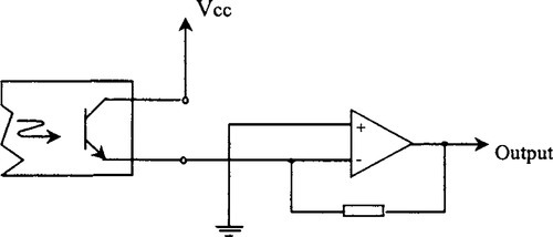
Phototransistors are designed to have a large base-collector junction area and a small emitter area. Some fraction of the photons that strike the base area cause the formation of electron-hole pairs in the base region. This fraction is called the quantum efficiency of the photodetector. If we ground the base and emitter (Figure 6-2(a)) and apply a positive voltage to the collector of the phototransistor, the device operates as a photodiode. The high field across the collector base junction quickly draws the electrons across into the collector region. The holes drift toward the base terminal, attracting electrons from the terminal. Therefore, a current flows from collector to base, causing a voltage drop across the load resistance (RL). The high junction capacitance, Ccb, results in an output circuit time constant RL Ccb, with a corresponding output voltage rise time. The output in this configuration is quite small and hence this connection normally is not used.
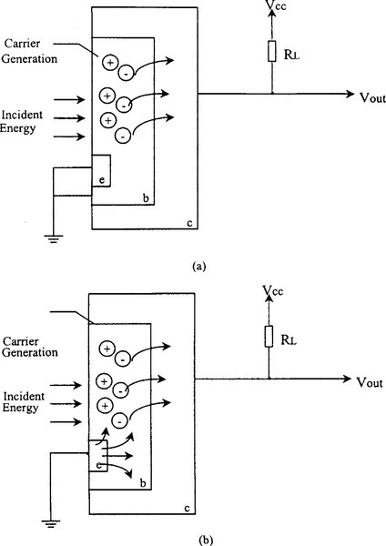
The most common circuit configuration is an open base connection (Figure 6-2(b)). With this connection, the holes generated in the base region cause the base potential to rise forward biasing the base-emitter junction. Electrons then are injected into the base from the emitter, trying to neutralize the excess holes. Because of the close proximity of the collector junction, the probability of an electron recombining with a hole is small and most of the injected electrons are immediately swept into the collector region. As a result, the total collector current is much higher than the photogenerated current and in fact is amplified β times. The total collector current is several hundred times greater than for the previous connection.
This gain comes with a penalty of much slower operation. Any drop in collector voltage is coupled to the base due to the collector/base capacitance which tends to turn off the injected current. The only current available to charge this junction capacitance is the original photocurrent. Thus, the rate of change of the output voltage is the same for both the diode and transistor connections. In the latter case, the voltage swing is β times as great, so the total rise time is β times as great as for the diode connection. Therefore, the effective output time constant is β RL Ccb. For the IL1, a typical two-wavelength rise time for 100 Ω results.
The ratio of the output current from the phototransistor (IC or IE) to the input current in the diode is called the current transfer ratio (CTR). For the IL1, the CTR is specified at 20% minimum with 35% being typical at IF = 10 mA. So, for a 10 mA input current the minimum output current is 2 mA. Another important parameter is that VF typically is 1.25 V at 60 mA IF.
6.4 Practical Circuits
Optos have many different applications. The following sections examine the most common digital and analog applications.
6.4.1 Digital Interfaces
In digital circuits, most common applications are output sensing circuits and input driving elements. We discuss some of the most important considerations in output sensing circuits and the input drivers.
6.4.1.1 Output Sensing Circuits
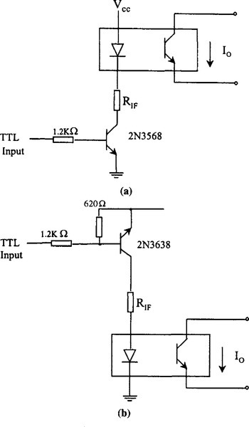
The output of the phototransistor can directly drive the input of standard logic circuits such as the 7400 TTL families. The worst case input current for the 74 series gate is –1.6 mA for VIN = 0.4 volts. This easily can be supplied by the output of an optocoupler such as the IL1 with 10 mA input to the infrared diode. Figure 6-3(a) shows a case with active level low circuit, and for higher speed, a smaller pull-up resistor can be used.
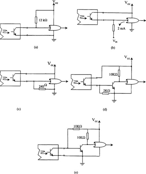
It is more difficult to operate into TTL gates in the active level high configuration. Figure 6-3(b) shows the best method when a negative supply is available. The circuit in Figure 6-3(c) requires 10 mA current from the optotransistor, with some sacrifice of the noise margin. The case in Figure 6-3(d) has a high sensitivity, needs extra parts, and still sacrifices the noise margin. Figure 6-3(e) also is a high-sensitivity circuit with extra parts.
Several optocoupler output transistors can be connected to perform logical functions. Figure 6-4 shows logical OR and logical AND connections, respectively.

6.4.1.2 Input Driving Circuits
The input side of an optocoupler such as the IL1 has a diode characteristic like that shown in Figure 6-5. The forward current must be controlled to provide the desired operating condition. The input can be conveniently driven by integrated circuit logic elements in a number of different ways. A few examples are given in Figure 6-6. The series resistor in Figure 6-6(a) can be omitted for about 15 mA into the diode.

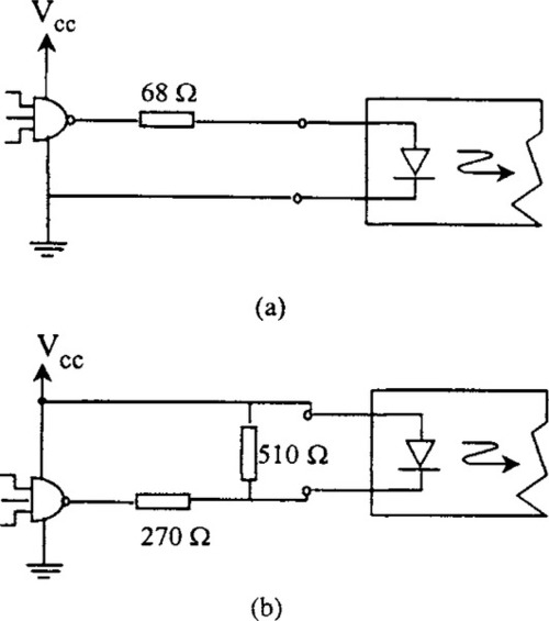
Obviously, many other ways may be used to drive the device with logic signals but the most common needs can be met with these circuits. All provide 10 mA into the LED, yielding a 2 mA minimum out of the phototransistor. The 1 V diode knee and its high capacitance (typically 100 pF) provide good noise immunity. The rise time and propagation delay can be reduced by biasing the diode to about 1 mA forward current, but the noise performance will be worse. These circuits have various advantages over other ways of doing the task, such as the use of relays, pulse transformers, and integrated circuit line drivers or receivers. Further details can be found in Siemens (1995-1996).
6.4.2 Linear Applications
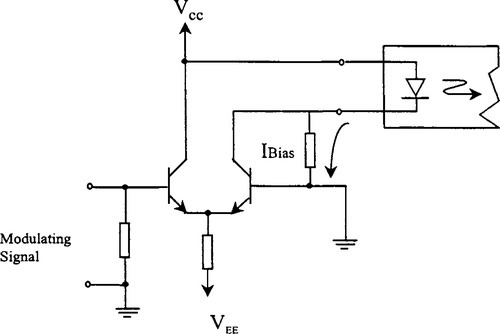
The curve of input current vs. output current for optoisolators is somewhat nonlinear, because of the variation of β with current for the phototransistor and the variation of infrared radiation out vs. forward current in the GaAs diode. The useful range of input current is about 1–100 mA (for devices such as the IL1 from Siemens), but higher currents may be used for short-duty cycles. For linear applications, the LED must be forward biased to some suitable current (usually 5–20 mA). Modulating signals then can be impressed on this DC bias. As shown in Figure 6-7, a differential amplifier is a good way to accomplish this.
Sensing in-linear applications can be done in several ways, depending on the requirements. For high-frequency performance, the phototransistor should be operated into a low-impedance input current amplifier. The simplest such scheme is a grounded base amplifier, as in Figure 6-8. The circuit will work equally well either way with a phase inversion between the two. Obviously, a PNP transistor would work as well.

A feedback amplifier also could be used to get a low-impedance input, as in Figure 6-9. For example, if R1 = 900 Ω, R2 = 100 Ω, and VCC = 5 V, we would have a current gain of 10 and an input impedance of about 6.3 Ω. This would give a considerable speed improvement over a 100 Ω load.

A high-speed operational amplifier could be used to give excellent performance, as in Figure 6-10. Note that, in all cases, the output can be taken from either the collector or the emitter of the phototransistor, depending on the polarity desired. The operating speed is the same in either case.
The design engineer will see many ways to expand on these circuits to achieve his or her goals. The devices are extremely versatile and can provide better ways to share many system problems than competing components. Special designs are possible to optimize certain parameters, such as coupling capacitance or transfer ratio.
6.5 Driving High-Level Loads with Optocouplers
Frequently, a load to be driven by an optocoupler requires more current, voltage, or both than an optocoupler can provide at its output. Available optocoupler output current is found by multiplying the input LED current by the CTR. For worst-case design, the minimum specified value should be used. Temperature derating usually is unnecessary over the 0–60°C range because the LED light output and transistor β have approximately compensating coefficients (for components similar to IL1). Multiplying the minimum CTR by 0.9 would ensure a safe design over this temperature range. More margin would be required over a wider range.
The LED source current is limited by its rated power dissipation. Table 6-1 shows the maximum allowable IF vs. maximum ambient temperature. The values for Table 6-1 are based on a 1.33 mW/°C derate from the 100 mW at 25°C power rating.
Table 6-1
Maximum forward diode current vs. temperature for the IL1, based on a derating factor of 1.33 mW/°C.
| Maximum Temperature (°C) | Ip Maximum (mA) |
| 40 | 50 |
| 60 | 35 |
| 80 | 17 |
(Reproduced by permission of Infineon Technologies.)
Based on the information in Table 6-1 and allowing a 10% margin for temperature effects, the minimum available output current for the IL1 will be 6.3 mA.
If the IL1 is being operated from logic with a 5 V driving transistor and 0.2 V VCE saturation is assumed for the driving transistor, a RIF resistor will provide the 48 mA. The forward voltage of the IR-emitting LED is about of 75R 1.2 V. Figure 6-11 shows two such drive circuits.
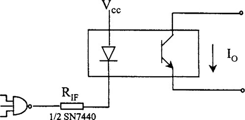
A “buffer gate” such as the SN7440 provides a very good alternative to discrete transistor drivers. Figure 6-12 shows how this is done. Note that the gate is used in the “current-sinking” rather than the “current-sourcing” mode. In other words, conventional current flows into the buffer gate to turn on the LED, because the TTL gate will sink more current than it will source. The SN7440 is specified to drive thirty 1.6 mA loads or 48 mA. Changing RIF from 75 Ω to 68 Ω adjusts for the higher saturation voltage of the monolithic device.
6.5.1 Higher-Load Current
For load currents greater than 6.3 mA, a current amplifier is required. Figure 6-13 shows two single-transistor current amplifier circuits.
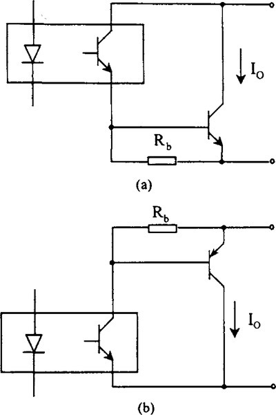
Since the transistor in the optocoupler is treated as a two-terminal device, no operational difference exists between the NPN and the PNP circuits. Rb provides a return path for ICBO of the output transistor. Its value is Rb = 400 mV/I CBO (T), where ICBO (T) is found for the highest junction temperature expected.
It is necessary to use the maximum dissipated power, the specified maximum junction-to-ambient thermal resistance, and the maximum design ambient temperature in conjunction with the specified maximum ICBO at 25°C to calculate ICBO (T), assuming that leakage currents double every ten degrees.
As an example, suppose a 2 N3568 is used to provide a 100 mA load current. Also assume a maximum steady-state transistor power dissipation of 100 mW and a 60°C maximum ambient temperature. The transistor junction-to-ambient thermal resistance is 333°C/W, so a maximum junction temperature of 93°C(60°C + 33°C) is expected. This is about seven decades above 25°C. Therefore, ICBO (T) = ICBO (max) × 27 = 50 mA × 128 = 6.5 μA. A safe value for Rb is 400 mV/6.5 μA = 62 kΩ.
Working backward, the maximum base current under load will be IO/hFE (min) = 100 mA/100 = 1 mA. The current in Rb is VBE /Rb = 600 mV/ 60 kΩ = 10 μA, which is negligible. An IL1 with a 9 mA drive would operate effectively. If the load requires more current than can be obtained with the highest β transistor available, then more than one transistor must be used in cascade. For example, suppose 3 A of load current and 10 W dissipation are needed. A Motorola MJE3055 (Q2) might be used for the output transistor, driven by an MJE205 (Q1), as shown in Figure 6-14. Using a 5°C/W heat sink and the rated MJE3055 junction-to-case thermal resistance of 1.4°C/W, we find that junction temperature rise is 64°C(6.4 × 10). Therefore maximum junction temperature is 124°C. This is ten decades above 25°C, making ICBO(T) = 210/cso(max) ![]() 103 ICBO(max).
103 ICBO(max).
ICBO (max) at 30 V or less is not given but ICEO is specified at a maximum of 0.7 mA for MJE3055. Using a value of 20 (for safety) for the minimum low-current hFE of the device, ICBO could be as large as ICEO /20 = 35 μA. Then ICBO (T) is 35 mA and Rb2 = 400 mV/35 mA = 11 Ω. For Ib use IO / hFE(min at 4 A) = 3 A/20 150 mA. IRb2 = 600 mV/10 Ω = 60 mA, so IE(Q1) = 210 mA.
Maximum power in Q1 will be about l/14th the power in Q2, since its current is lower by that ratio and the two collector-to-emitter voltages are nearly the same. This means Q1 must dissipate 700 mW. Assuming a small “flag-type” heat sink having 50°/W thermal resistance, we find the junction temperature at about 95°C. The 150°C case temperature ICBO rating for this device is 2 mA, so one can work backward and assume about 1/30 of this value, or 70 μA. On the other hand, the 25°C-rated ICBO is 100 μA. Choosing the larger of these contradictory specifications, Rb1 = 400 mV/0.1 mA = 4 k ≈ 3.9 k. The Q1 base current is IE(Q1)/hFE(Q1-min) = 210 mA/50 = 4.2 mA. Total current is Ib(Q1) + IRb1 = 4.2 + 0.24 = 4.5 mA. An IL1 could be used here.
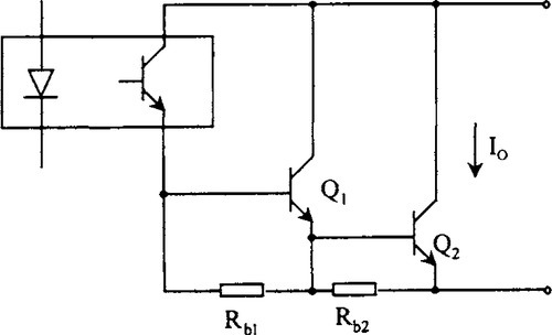
6.5.2 Higher-Load Voltages
All the current gain circuits shown so far have one common feature: The load voltage is limited by the voltage rating of the optocoupler and not by the voltage or power rating of the transistor(s). Figure 6-15(a) shows a method of overcoming this limitation. This circuit will stand off BVCEO of Q1. The voltage rating of the phototransistor is irrelevant since its maximum collector-emitter voltage is the base-emitter voltage of Q1 (about 0.7 V). Unlike the Darlington configurations shown previously, this circuit operates “normally-on.” When no current flows in the LED and the phototransistor is off, R1 current is allowed to flow into the base of Q1, turning on Q1. When the optocoupler is energized, its phototransistor “shorts out” the R1 current, turning off Q1.
The value of R1 depends only on the load-supply voltage (Vcc+ – Vcc−) and the maximum required base current for Q1. This is derived from the minimum β of Q1 at minimum temperature and the load current. The required current-drive capability is the same as IR1, since IR1 changes negligibly when the circuit goes between its on and off states.
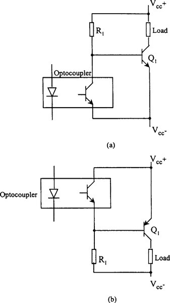
In some applications either more current gain will be required than one transistor can provide or the power dissipated in R1 will be objectionable. In these cases, use of Darlington high-voltage boosters (as shown in Figure 6-16(a)) is a solution. If more than one load is being driven and the negative terminals must be in common, it is necessary to use the PNP circuit, as per Figure 6-16(b). Otherwise, the NPN is better because the transistors cost less. Performance characteristics of the NPN and PNP versions are identical if the device parameters are the same.

6.5.3 Higher Speed
Figure 6-17 shows a typical circuit employing an optocoupler to transmit logic signals between electrically isolated parts of a system. In the circuit shown, the optocoupler must “sink” the current from one TTL load plus a pull-up resistor to VCC .The resistor in series with the LED of the optocoupler must supply the worst-case load current divided by the CTR of the optocoupler. If an optocoupler is used with a minimum CTR of 0.2 and 80% variation in the load is allowed, 8.1 mA is required. This is supplied by the 430 Ω resistor.
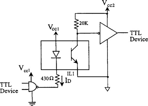
The maximum repetition rate at which this circuit will operate is only about 8 kHz. This severe limitation is due entirely to the characteristics of the phototransistor half of the optocoupler. The device has a large base-collector junction area and a very thick base region to make it sensitive to light. Cob typically is 25 pF. This capacitance in the circuit of Figure 6-17 is effectively multiplied by a large factor due to the “Miller effect.” Also, because the base region volume is large, base storage time is large.
A very simple method of reducing both effects is to add a resistor between the base and the emitter, as shown in Figure 6-18. This resistor helps by reducing the time constant due to Cob and removing stored charge from the base region faster than recombination. When a base-emitter resistor is used, the required LED drive is increased, since much of the photo current generated in the base-collector junction is deliberately “dumped.”
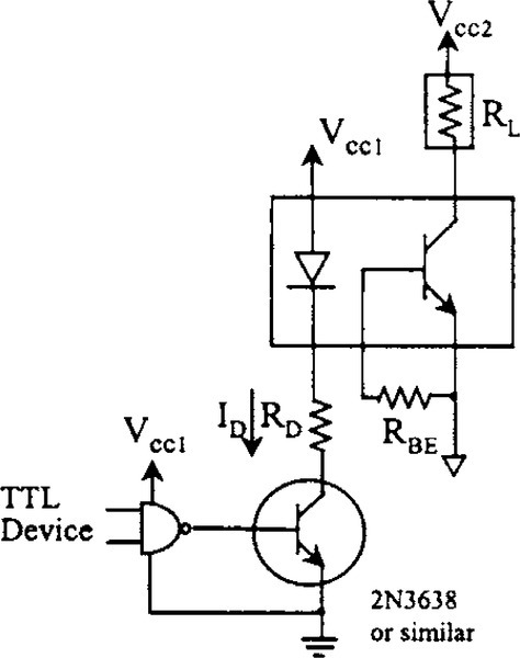
Using this method usually does not result in a large power supply current drain, since the average repetition rate is low in most applications. As the drive is increased and RBE is reduced, turn-on and turn-off time both decrease. The total amount of charge stored can be reduced by decreasing the LED drive pulse duration. Also, as higher drive levels are used, the load resistance, RL, can be reduced to further enhance the speed of the circuit. These parameters are related to each other such that all should be changed together for best results. One important generalization can be made concerning their interdependence. The LED drive pulse duration, –Tin, output fall time (tf), output rise time (tr), and propagation delay (tp) should occur in a 1.5:1:1:1 ratio, approximately. If this relationship does not occur, the circuit will not operate at as high a repetition rate as it could at the same drive level. Output pulse duration, Tout, equals Tin at low currents but stretches out at high currents.
Figure 6-19 shows graphs relating the important parameters for a typical optoisolator such as the IL1. The optimum values of Tin, RBE, and RL are shown vs. LED pulse current, as are the resulting output pulse width and maximum full-swing frequency. Rise, fall, and propagation times can be read as two-thirds of Tin. Figure 6-19 shows that increasing drive to 200 mA and using optimum RBE and RL will increase the maximum repetition rate from 3 kHz to 500 kHz, a 167:1 improvement.

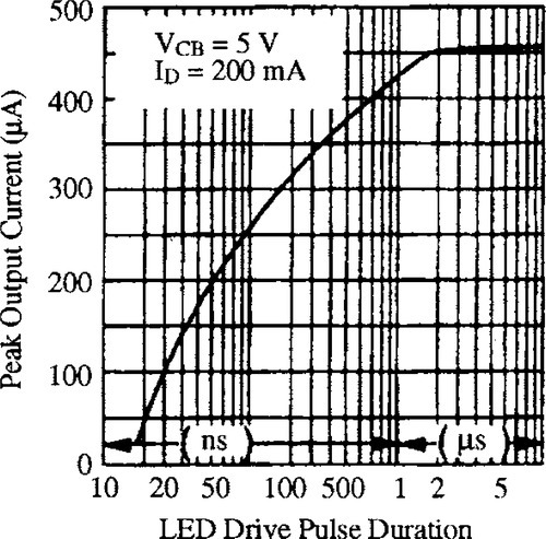
Lower-grade optocouplers will behave similarly if the LED drive level is scaled appropriately to allow for a lower CTR. Another method of increasing speed is to operate the phototransistor as a photodiode. In this method, the bias voltage is supplied between the collector and base terminal, the emitter being unused. Operation to at least 1.0 MHz is possible this way, but external amplification is necessary. Figure 6-20 is a graph showing peak output current vs. drive pulse duration for 200 mA peak drive current.
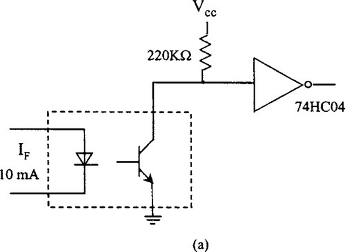
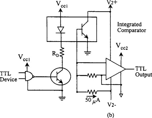
Since output current is small, some type of wide bandwidth amplifier must be employed to drive TTL loads. One simple solution for intermediate-speed operation is the use of a MOS inverter (1/6 74HC04), as per Figure 6-21(a). Another device that will provide a good inter face is an integrated comparator amplifier as in Figure 6-21 (b).
6.6 Photovoltaic Devices
6.6.1 Photovoltaic Isolators
A photovoltaic isolator (PVI) generates an electrically isolated voltage on a receipt of an input signal. Conventional photocouplers merely modulate the resistance of an output device such as a transistor, diode, or resistor. Such photocouplers require a separate voltage source to detect the presence of an input signal. In contrast, a PVI actually transmits (and transforms) energy across the isolation barrier and directly generates an output voltage. This DC voltage, available at a 2500 VAC isolation level, gives circuit designers a new and uniquely useful electronic component.
The input of the PVI is an LED optically coupled to, but electrically isolated from, the output. A GaAlAs LED is used for high output and maximum stability. The infrared emission from the LED energizes, by photovoltaic action, a series connection of silicon PN junctions. A unique alloyed junction stack, which is edge illuminated, is used to form the output photovoltaic generators. This novel structure produces extremely high operating efficiency.
A PVI can serve as an isolator, coupler, or isolated voltage source. As an isolator, the PVI can be the key component in a solid-state relay circuit. The PVI is ideally suited for driving power MOSFETs or sensitive gate SCRs to form solid-state relays. As a coupler, the PVI can sense a low-level DC signal and transmit a voltage signal to an electrically remote circuit. As a voltage source, the PVI can function as a “DC transformer” by providing an isolated, low-current DC source for basing or supplying power to low quiescent current electronic devices.
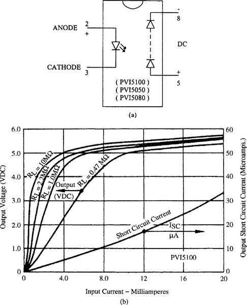
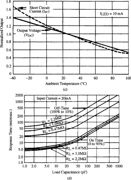
An example of these are the PVI series microelectronic isolators from International Rectifier. The PVI 5100, PVI 5050, and PVI 1050 are typical devices. These units are available with single (PVI 5100, PVI 5050) or dual (PVI 1050) 5 V output, which can be series connected to produce 10 V. Figure 6-22 depicts characteristics of these devices.
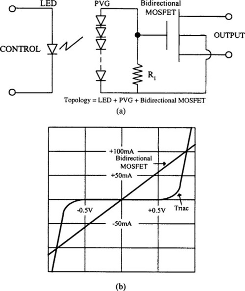
Recent developments in semiconductor technology have led to the design of a new type of solid-state relay, which combines photovoltaic isolation with MOSFET power-integrated circuit techniques.
This new topology, photovoltaic relay (PVR), which evolved recently, is illustrated in Figure 6-23. The PVR topology achieves electro-optical isolation by means of a light-emitting diode energizing a photovoltaic generator (PVG) consisting of a series connection of silicon P-N junctions. The signal from the photovoltaic generator in turn activates a bidirectional MOSFET configuration. A PVR configuration achieves a unique combination of operating advantages not present in any other relay. The PVR has the solid-state advantages of long switching life, high operating speed, low pickup power, bounce-free operation, noninductive input, insensitivity to position and magnetic fields, extreme shock and vibration resistance, and miniaturization. In addition, modem MOSFET technology provides a much better equivalent (of an analog electromechanical) switch than thyristor or bipolar transistor technology used dominantly as the output contact in previous solid-state relays. Relative to thyristors, the MOSFET displays a linear on-resistance rather than a 0.6 V threshold in forward conduction, as shown in Figure 6-23(b). An inverse series connection of two MOSFETs can switch DC or AC at frequencies well into the RF range. Static and commutating dv/dt effects are not inherent and turn-off can be instantaneous. Relative to bipolar transistors, MOSFETs display lower on-state offset voltages, much lower off-state leakages, and, most important, have essentially infinite static forward current gain (i.e., MOSFETs are voltage controlled).
6.7 Conclusion
This chapter is an introduction to the use of optocouplers as a low-cost solution to achieve galvanic isolation between different circuits and provide sufficient isolation voltage between circuits. Information is based mostly on literature from the Siemens (1995–1996) Optoelectronics Division (Infineon Technologies is the present name of the company). Using the fundamentals presented here, a designer should be able to use many different versions of optoisolator circuits for different applications and speeds. The following references provide more detail.