
Data Converters
3.1 Introduction
Modern design trends use the power and precision of the digital world of components to process analog signals. However, the link between the digital/processing world and the analog/real world is based on analog-to-digital and digital-to-analog converter ICs, which generally are grouped as the data converters.
Until about 1988, engineers have had to stockpile their most innovative A/D converter (ADC) designs, because available manufacturing processes simply could not implement those designs onto monolithic chips economically. Prior to 1988, except for the introduction of successive approximation and integrating and flash ADCs, the electronics industry saw no major changes in monolithic ADCs. Since then, manufacturing processes caught up with the technology and many techniques such as subranging flash, self-calibration, delta/sigma, and many other special techniques have been implemented on monolithic chips.
High-speed ADCs are used in a wide variety of real-time digital signal processing (DSP) applications, replacing systems that used analog techniques alone. The major reasons for using DSP are that the cost of the processors has gone down, their speed and computational power have increased, and they are reprogrammable, allowing for system performance upgrades without hardware changes. DSP offers practical solutions that cannot be easily achieved in the analog domain; for example, V.32 and V.34 modems.
This chapter provides an overview of design concepts and application guidelines for systems using modern analog/digital and digital/analog converters implemented on monolithic chips.
3.2 Sampled Data Systems
To specify intelligently the ADC portion of the system, one must first understand the fundamental concepts of sampling and quantization and their effects on the signal.
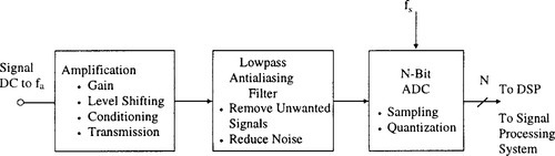
Let us consider the traditional problem of sampling and quantizing a baseband signal whose bandwidth lies between DC and an upper frequency of interest, fs. This often is referred to as Nyquist or sub-Nyquist sampling. The topic of super-Nyquist sampling (sometimes called undersampling), where the signal of interest falls outside the Nyquist bandwidth (DC to fs/2) is treated later. Figure 3-1 shows key elements of a baseband sampled data system.
3.2.1 Discrete Time Sampling of Analog Signals
Figure 3-2 shows the concept of discrete time and amplitude sampling of an analog signal. The continuous analog data must be sampled at discrete intervals, ts, which must be carefully chosen to ensure an accurate representation of the original analog signal. It is clear that, the more samples taken (faster sampling rates), the more accurate the digital representation; and if fewer samples are taken (slower sampling rates), a point is reached where critical information about the signal actually is lost.

To discuss the problem of losing information in the sampling process, it is necessary to recall Shannon’s information theorem and Nyquist’s criteria. Shannon’s information theorem:
• An analog signal with a bandwidth of fa must be sampled at a rate of fs > 2 fa to avoid loss of information.
• The signal bandwidth may extend from DC to fa (baseband sampling) or from f1 to f2, where fa = f2 − f1 (undersampling, or super-Nyquist sampling).
• Nyquist criteria:
• If fs < 2fa, then a phenomenon called aliasing will occur.
• Aliasing is used to advantage in undersampling applications.
3.2.1.1 Implications of a Aliasing
To understand the implications of aliasing in both the time and frequency domains, first consider the case of a time domain representation of a sampled sine wave signal shown in Figure 3-3. In Figures 3-3(a) and 3-3(b), it is clear that an adequate number of samples have been taken to preserve the information about the sine wave. Figure 3-3(c) represents the ambiguous limiting condition where fs = 2fa If the relationship between the sampling points and the sine wave is such that the sine wave is being sampled at precisely the zero crossings (rather than at the peaks, as shown in the illustration), then all information regarding the sine wave would be lost. Figure 3-3(d) represents the situation where fs < 2fa, and the information obtained from the samples indicates a sine wave having a frequency lower than fs/2. This is a case where the out-of-band signal is aliased into the Nyquist bandwidth between DC and fs/2. As the sampling rate is further decreased and the analog input frequency fa approaches the sampling frequency fs, the aliased signal approaches DC in the frequency spectrum.

Let us look at the corresponding frequency domain representation of each case. From each case of frequency domain representation, we make the important observation that, regardless of where the analog signal being sampled happens to lie in the frequency spectrum, the effects of sampling will cause either the actual signal or an aliased component to fall within the Nyquist bandwidth between DC and fs/2. Therefore, any signals that fall outside the bandwidth of interest, whether they be spurious tones or random noise, must be adequately filtered before sampling. If unfiltered, the sampling process will alias them back within the Nyquist bandwidth, where they will corrupt the wanted signals.
3.2.1.2 High-Speed Sampling
Now let us discuss the case of high-speed sampling, analyzing it in the frequency domain. First, consider the use of a single-frequency sine wave of frequency fa sampled at a frequency fs by an ideal impulse sampler (see Figure 3-4(a)). Also assume that fs > 2fa as shown. The frequency domain output of the sampler shows aliases or images of the original signal around every multiple of fs; that is, at frequencies equal to
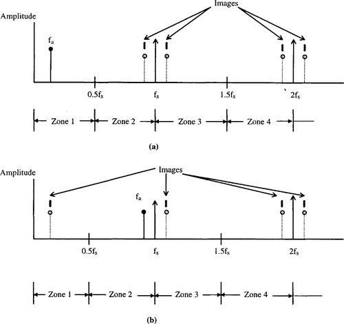
The Nyquist bandwidth, by definition, is the frequency spectrum from DC to fs/2. The frequency spectrum is divided into an infinite number of Nyquist zones, each having a width equal to 0.5 fs, as shown.
Now consider a signal outside the first Nyquist zone, as shown in Figure 3-4(b). Notice that, even though the signal is outside the first Nyquist zone, its image (or alias), fs – fa, falls inside. Returning to Figure 3-4(a), it is clear that, if an unwanted signal appears at any of the image frequencies of fa, it also will occur at fa, thereby producing a spurious frequency component in the Nyquist zone. This is similar to the analog mixing process and implies that some filtering ahead of the sampler (or ADC) is required to remove frequency components that are outside the Nyquist bandwidth but whose aliased components fall inside it. The filter performance will depend on how close the out-of-band signal is to fs/2 and the amount of attenuation required.
3.2.1.3 Antialiasing Filters
Baseband sampling implies that the signal to be sampled lies in the first Nyquist zone. It is important to note that, with no input filtering at the input of the ideal sampler, any frequency component (either signal or noise) that falls outside the Nyquist bandwidth in any Nyquist zone will be aliased back into the first Nyquist zone. For this reason, an antialiasing filter is used in almost all sampling ADC applications to remove these unwanted signals.
Properly specifying the antialiasing filter is important. The first step is to know the characteristics of the signal being sampled. Assume that the highest frequency of interest is fa. The antialiasing filter passes signals from DC to fa while attenuating signals above fa. Assume that the corner frequency of the filter is chosen to be equal to fa. The effect of the finite transition from minimum to maximum attenuation on system dynamic range (DR) is illustrated in Figure 3-5.
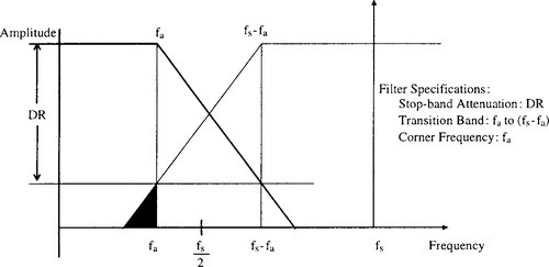
Assume that the input signal has full-scale components well above the maximum frequency of interest, fa. The diagram shows how full-scale frequency components above fs – fa are aliased back into the bandwidth DC to fa. These aliased components are indistinguishable from actual signals and therefore limit the dynamic range to the value on the diagram, which is shown as DR.
The antialiasing filter transition band therefore is determined by the comer frequency fa, the stop band frequency (fs – fa), and the stop band attenuation DR. The required system dynamic range is chosen based on our requirement for signal fidelity.
Filters have to become more complex as the transition band becomes sharper, all other things being equal. For instance, a Butterworth filter gives 6 dB attenuation per octave for each filter pole. Achieving 60 dB attenuation in a transition region between 1 and 2 MHz (1 octave) requires a minimum of ten poles. This is not a trivial filter and definitely a design challenge. Therefore, other filter types generally are better suited to high-speed applications where the requirement is for a sharp transition band and in-band flatness coupled with linear phase response. Elliptic filters meet these criteria and are a popular choice.
From this discussion, we can see how the sharpness of the antialiasing transition band can be traded off against the ADC sampling frequency. Choosing a higher sampling rate (oversampling) reduces the requirement on transition band sharpness (hence, the filter complexity) at the expense of using a faster ADC and processing data at a faster rate. This is illustrated in Figure 3-6, which shows the effects of increasing the sampling frequency while maintaining the same analog corner frequency, fa, and the same dynamic range, DR, requirement.

Based on this discussion one could start the design process by selecting a sampling rate of two to four times fa. Filter specifications could be determined from the required dynamic range based on cost and performance. If such a filter is not realizable, a high sampling rate with a faster ADC will be required.
The antialiasing filter requirements can be relaxed somewhat if it is certain that there never will be a full-scale signal at the stop band frequency, fs – fa. In many applications, it is improbable that full-scale signals will occur at this frequency. If the maximum signal at the frequency fs – fa will never exceed X dB below full scale, the filter stop band attenuation requirement is reduced by that amount. The new requirement for stop band attenuation at fs – fa based on this knowledge of the signal now is only (DR − X) dB. When making this type of assumption, be careful to treat any noise signals that may occur above the maximum signal frequency, fa, as unwanted signals that also alias back into the signal bandwidth.
Properly specifying the antialiasing filter requires a knowledge of the signal’s spectral characteristics as well as the system’s dynamic range requirements. Consider the signal in Figure 3-6(c), which has a maximum full-scale frequency content of fa = 35 kHz sampled at a rate of fs = 100 kS/s. Assume that the signal has the spectrum shown in Figure 3-6(c) and is attenuated by 30 dB at 65 kHz (fs – fa). Observe that the system dynamic range is limited to 30 dB at 35 kHz because of the aliased components. If additional dynamic range is required, an antialiasing filter must be provided to provide more attenuation at 65 kHz. If a dynamic range of 74 dB (12 bits) at 35 kHz is desired, then the antialiasing filter attenuation must go from 0 dB at 35 kHz to 44 dB at 65 kHz. This is an attenuation of 44 dB in approximately one octave; therefore, a sevenpole filter is required. (Each filter pole provides approximately 6 dB attenuation per octave.)
One must consider that broadband noise may be present with the signal, which also can alias within the bandwidth of interest. This is especially true with wideband op amps that provide low distortion levels.
3.2.2 ADC Resolution and Dynamic Range Requirements
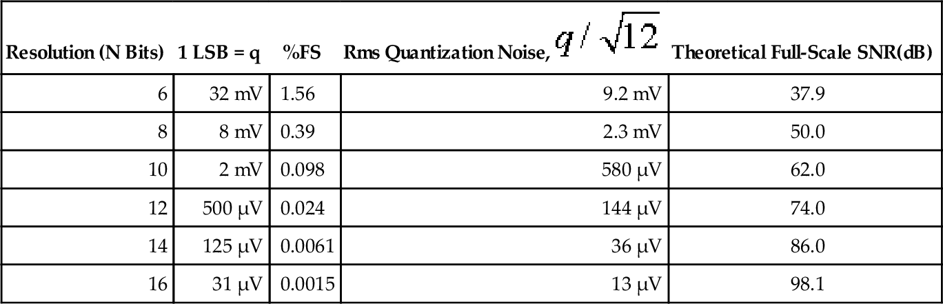
Having discussed the sampling rate and filtering, we next discuss the effects of dividing the signal amplitude into a finite number of discrete quantization levels. Table 3-1 shows relative bit sizes for various resolution ADCs, for a full-scale input range chosen as approximately 2 V, which is popular for higherspeed ADCs. The bit size in determined by dividing the full-scale range (2.048 V) by 2N.
Table 3-1
Bit Sizes, Quantization Noise, and Signal-to-Noise Ratio (SNR) for 2.048 V Full-Scale Converters
| Resolution (N Bits) | 1 LSB = q | %FS | Rms Quantization Noise, | Theoretical Full-Scale SNR(dB) |
| 6 | 32 mV | 1.56 | 9.2 mV | 37.9 |
| 8 | 8 mV | 0.39 | 2.3 mV | 50.0 |
| 10 | 2 mV | 0.098 | 580 μV | 62.0 |
| 12 | 500 μV | 0.024 | 144 μV | 74.0 |
| 14 | 125 μV | 0.0061 | 36 μV | 86.0 |
| 16 | 31 μV | 0.0015 | 13 μV | 98.1 |
The selection process for determining the ADC resolution should begin by determining the ratio between the largest signal (full-scale) and smallest signals you wish the ADC to detect. Convert this ratio to dB and divide by 6. This is your minimum ADC resolution requirement for DC signals. You actually will need more resolution to account for extra signal headroom, since ADCs act as hard limiters at both ends of their range. Remember that this computation is for DC or low-frequency signals and that the ADC performance will degrade as the input signal slew rate increases. The final ADC resolution actually will be dictated by dynamic performance at high frequencies. This may lead to the selection of an ADC with more resolution at DC than is required.
Table 3-1 also indicates the theoretical rms quantization noise produced by a perfect N-bit ADC. In this calculation, the assumption is that quantization error is uncorrelated with the ADC input. With this assumption, the quantization noise appears as random noise spread uniformly over the Nyquist bandwidth, DC to fs/2, and it has an rms value equal to ![]() Other cases may be different, and some practical explanation is given in Analog Devices (1995).
Other cases may be different, and some practical explanation is given in Analog Devices (1995).
3.2.3 Effective Number of Bits of a Digitizer
Table 3-1 shows the theoretical full-scale SNR calculated for the perfect N-bit ADC, based on the formula
Various error sources in the ADCs cause the measured SNR to be less than the theoretical value shown in equation (3.2). These errors are due to integral and differential nonlinearities, missing codes, and internal ADC noise sources (some of which are discussed later).
In addition, the errors are a function of the input slew rate and therefore increase as the input frequency gets higher. In calculating the rms value of the noise, it is customary to include the harmonics of the fundamental signal. This sometimes is referred to as the signal-to-noise-and-distortion, S/(N + D) or SINAD, but usually simply as SNR.
This leads to the definition of another important ADC dynamic specification, the effective number of bits (ENOB). The effective bits are calculated by first measuring the SNR of an ADC with a full-scale sine wave input signal. The measured SNR (SNRactual or SINAD) is substituted into the equation for SNR, and the equation is solved for N as shown next:

For a typical ADC, the AD676 from Analog Devices (a 16-bit ADC) is shown in Figure 3-7.

For this device, the SNR value of 88 dB corresponds to approximately 14.3 effective bits (for 0 dB input), while it drops to 6.4 ENOB at 1 MHz. The methods for calculating ENOB, SNR, and other parameters are described in Analog Devices (1992,Chapter 7) and Tektronix (1986).
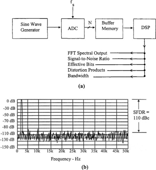
In testing ADCs, the SNR usually is calculated using DSP techniques while applying a pure sine wave signal to the input of ADC. A typical test system is shown in Figure 3-8(a). The fast Fourier transform (FFT) processes a finite number of time samples and converts them into a frequency spectrum such as the one shown in Figure 3-8(b) for an AD676-type 16-bit 100 kSPS sampling ADC. The frequency spectrum then is used to calculate the SNR as well as the harmonics of the fundamental input signal.
The rms value of the signal is first computed. The rms value of all other frequency components over the Nyquist bandwidth (this includes not only noise but also distortion products) is computed. The ratio of these two quantities, expressed in decibels is the SNR. Various error sources in the ADC cause the measured SNR to be less than the theoretical value, 6.02N + 1.76 dB.
3.2.3.1 Spurious Components and Harmonics
The peak spurious or peak harmonic component is the largest spectral component excluding the input signal and DC. This value is expressed in decibels relative to the rms value of a full-scale input signal as was shown in Figure 3-8(a). The peak spurious specification also occasionally is referred to as the spurious free dynamic range (SFDR). SFDR usually is measured over a wide range of input frequencies and at various amplitudes. It is important to note that the harmonic distortion or SFDR of an ADC is not limited by its theoretical SNR value. The SFDR of a 12-bit ADC may exceed 85 dB, while the theoretical SNR is only 74 dB. On the other hand, the SINAD of the ADC may be limited by poor harmonic distortion performance, since the harmonic components are included with the quantization noise when computing the rms noise level. The SFDR of an ADC is defined as the ratio of the rms signal amplitude to the rms value peak spurious spectral content (measured over the entire first Nyquist zone, DC to fs/2). The SFDR generally is plotted as a function of signal amplitude and may be expressed relative to the signal amplitude (dBc) or the ADC full scale (dBFS).
For a signal near full scale, the peak spectral spur generally is determined by one of the first few harmonics of the fundamental input signal. However, as the signal falls several decibels below full scale, other spurs generally occur that are not direct harmonics of the input signal due to the differential nonlinearity of the ADC transfer function. Therefore, the SFDR considers all sources of distortion, regardless of their origin.
The total harmonic distortion (THD) is the ratio of the rms sum of the harmonic components to the rms value of an input signal, expressed in a percentage or decibels. For input signals or harmonics above the Nyquist frequency, the aliased components are used in making the calculation. The THD usually is measured at several input signal frequencies and amplitudes. Figure 3-9 shows the SFDR performance of a 12-bit, 41 MSPS wideband ADC designed for communication applications (AD9042 from Analog Devices).
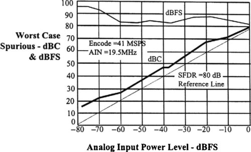
Note that a minimum of 80 dBc SFDR is obtained over the entire first Nyquist zone (DC to 20 MHz). The plot also shows SFDR expressed as dBFS. The SFDR generally is much greater than the ADCs theoretical N-bit SNR (6.02N + 1.76 dB). For example, the AD9042 is a 12-bit ADC with an SFDR of 80 dBc and a typical SNR of 65 dBc (the theoretical SNR is 74 dB). This is due to the fundamental distinction between noise and distortion measurements.
3.3 A/D Converter Errors
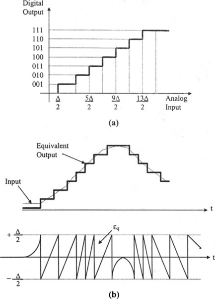
First, let us look at how bits are assigned to the corresponding analog values in a typical analog-to-digital converter. The method of assigning bits to the corresponding analog value of the sampled point often is referred to as quantization (see Figure 3-10(a)). As the analog voltage increases, it crosses transitions of “decision levels,” which causes the ADC to change state. In an ideal ADC, the transitions are at half-unit levels, with Δ representing the distance between the decision levels. The Δ is often is referred to as the bit size or quantization size. The fact that Δ always has a finite size leads to uncertainty, since any analog value within the finite range can be represented. This quantization uncertainty is expressed as plus or minus half the least significant bit (LSB) as shown in Figure 3-10(b). As this plot shows, the output of an ADC may be thought of as the analog signal plus some quantizing noise. The more bits the ADC has, the less significant this noise becomes.

Certain parameters limit the rate at which an ADC can acquire a sample of the input waveform: the acquisition turn-on delay, acquisition time, sample or track time, and hold time. Figure 3-10(c) shows a graphic representation of the acquisition cycle of a typical ADC. The turn-on time (the time the device takes to get ready to acquire a sample) is the first event. The acquisition time is next. This is the time the device takes to get to the point at which the output tracks the input sample, after the sample command or clock pulse. The aperture time delay is the time that elapses between the hold command and the point at which the sampling switch is completely open. The device then completes the hold cycle and the next acquisition is taken.
This process indicates that the real world of acquisition is not an ideal process at all, and the value sampled and converted could have some sources of error. Most of these errors increase with the sampling rate.
The approximation or “rounding” effect in A/D converters is called quantization, and the difference between the original input and the digitized output, the quantization error, is denoted here by εq. For the characteristic of Figure 3-10(a), εq varies as shown in Figure 3-10(b), with the maximum occurring before each code transition. This error decreases as the resolution increases, and its effect can be viewed as additive noise (quantization noise) appearing at the output. Thus, even an “ideal” m-bit ADC introduces nonzero noise in the converted signal simply due to quantization.
We can formulate the impact of quantization noise on the performance as follows. For simplicity, consider a slightly different input/output characteristic, shown in Figure 3-11(a), where code transitions occur at odd (rather than even) multiples of Δ/2. A time domain waveform therefore experiences both negative and positive quantization errors, as illustrated in Figure 3-11(b). To calculate the power of the resulting noise, we assume that εq is (i) a random variable uniformly distributed between − Δ/2 and + Δ/2, and (ii) independent of the analog input. While these assumptions are not strictly valid in the general case, they usually provide a reasonable approximation for resolutions above four bits. Razavi (1995) provides more details and the derivations of equations (3.2) and (3.3).
Full specification of the performance of ADCs requires a large number of parameters, some of which are defined differently by different manufacturers. Some important parameters frequently used in component data sheets and the like are described here. Figure 3-12 could be used to illustrate parameters such as differential nonlinearity (DNL), integral nonlinearity (INL), and offset and gain errors — all static parameters of the ADC process.

3.3.1
3.3.1.1 Differential Nonlinearity
Differential nonlinearity is the maximum deviation in the difference between two consecutive code transition points on the input axis from the ideal value of 1 LSB. The DNL is a measure of the deviation code widths from the ideal value of 1 LSB.
3.3.1.2 Integral Nonlinearity
The INL is the maximum deviation of the input/output characteristic from a straight line passed through its end points (line AB in Figure 3-12). The overall difference plot is called the INL profile. The INL is the deviation of code centers from the converter’s ideal transfer curve. The line used as the reference may be drawn through the end points or may be a best-fit line calculated from the data.
The DNL and INL degrade as the input frequency approaches the Nyquist rate. The DNL shows up as an increase in quantization noise, which tends to elevate the converter’s overall noise floor. Theoretical quantization noise for an ideal converter with the Nyquist bandwidth is
where q is the weight of the LSB.
At the same time, because the INL appears as a bend in the converter’s transfer curve, it generates spurious frequencies (spurs) not in the original signal information. The testing of ADC linearity parameters is discussed in Shill (1995).
3.3.1.3 Offset Error and Gain Error
The offset is a vertical intercept of the straight line through the end points. The gain error is the deviation of the slope of line AB from its ideal value (usually unity).
3.3.1.4 Testing of ADCs
A known periodic input is converted by an ADC under test at sampling times that are asynchronous relative to the input signal. The relative number of occurrences of the distinct digital output codes is termed the code density. For an ideal ADC, the code density is independent of the conversion rate and input frequency. These data are viewed in the form of a normalized histogram showing the frequency of occurrence of each code from zero to full scale. The code density data are used to compute all bit transition levels. Linearity, gain, and offset errors are readily calculated from a knowledge of the transition levels. This provides a complete characterization of the ADC in the amplitude domain.
The effect of some of these static errors in the frequency domain for high-speed ADCs is discussed in Louzon (1995). Doernberg, Lee, and Hodges (1984) provide ADC characterization methods based on code density test and spectral analysis using FFT.
3.4 Effects of Sample and Hold Circuits
The sample and hold amplifier (SHA) is a critical part of many data acquisition systems. It captures an analog signal and holds it during some operation (most commonly during analog-to-digital conversion). The circuitry involved is demanding, and unexpected properties of commonplace components such as capacitors and printed circuit boards may degrade SHA performance.
When a sample and hold amplifier is in the sample mode, the output follows the input with only a small voltage offset. In some SHAs, the output during the sample mode does not follow the input accurately and the output is accurate only during the hold period.
Today, high-density IC processes allow the manufacture of ADCs containing an integral SHA. Wherever possible, ADCs with an integral SHA (often known as sampling ADCs) should be used in preference to separate ADCs and SHAs. The advantage of such a sampling ADC – apart from the obvious ones of smaller size, lower cost, and fewer external components – is that the overall performance is specified. The designer need not spend time ensuring that no specification, interface, or timing issues are involved in combining a discrete ADC and a discrete SHA.
3.4.1 Basic SHA Operation
Regardless of the circuit details or type of SHA in question, all such devices have four major components. The input amplifier, energy storage device (capacitor), output buffer, and switching circuits are common to all SHAs, as shown in the typical configuration of Figure 3-13(a).
The energy storage device, the heart of the SHA, almost always is a capacitor. The input amplifier buffers the input by presenting a high impedance to the signal source and providing current gain to charge the hold capacitor. In the track mode, the voltage on the hold capacitor follows (or tracks) the input signal (with some delay and bandwidth limiting). Figure 3-10 depicts this process. In the hold mode, the switch is opened and the capacitor retains the voltage present before it was disconnected from the input buffer. The output buffer offers a high impedance to the hold capacitor to keep the held voltage from discharging prematurely. The switching circuit and its driver form the mechanism by which the SHA is alternately switched between track and hold.
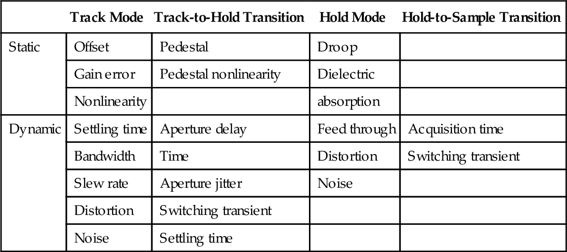
Four groups of specifications describe basic SHA operation: track mode, track-to-hold transition, hold mode, and hold-to-track transition. These specifications are summarized in Table 3-2, and some of the SHA error sources are shown in Figure 3-13(b). Because of both DC and AC performance implications for each of the four modes, properly specifying an SHA and understanding its operation in a system are complex matters.
Table 3-2
Sample and Hold Specifications
| Track Mode | Track-to-Hold Transition | Hold Mode | Hold-to-Sample Transition | |
| Static | Offset | Pedestal | Droop | |
| Gain error | Pedestal nonlinearity | Dielectric | ||
| Nonlinearity | absorption | |||
| Dynamic | Settling time | Aperture delay | Feed through | Acquisition time |
| Bandwidth | Time | Distortion | Switching transient | |
| Slew rate | Aperture jitter | Noise | ||
| Distortion | Switching transient | |||
| Noise | Settling time |
3.4.1.1 Track Mode Specifications
Since an SHA in the sample (or track) mode is simply an amplifier, both the static and dynamic specifications in this mode are similar to those of any amplifier. The principal track mode specifications are offset, gain, nonlinearity, bandwidth, slew rate, settling time, distortion, and noise; however, distortion and noise in the track mode often are of less interest than in the hold mode. Fundamental amplifier specifications are discussed in Chapter 2.
3.4.1.2 Track-to-Hold Mode Specifications
When the SHA switches from track to hold, generally a small amount of charge is dumped on the hold capacitor because of nonideal switches. This results in a hold mode DC offset voltage called pedestal error. If the SHA is driving an ADC, the pedestal error appears as a DC offset voltage that may be removed by performing a system calibration. If the pedestal error is a function of the input signal level, the resulting nonlinearity contributes to hold mode distortion. Pedestal errors may be reduced by increasing the value of the hold capacitor with a corresponding increase in acquisition time and a reduction in bandwidth and slew rate.
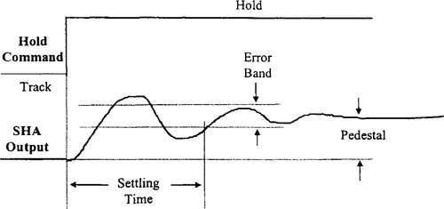
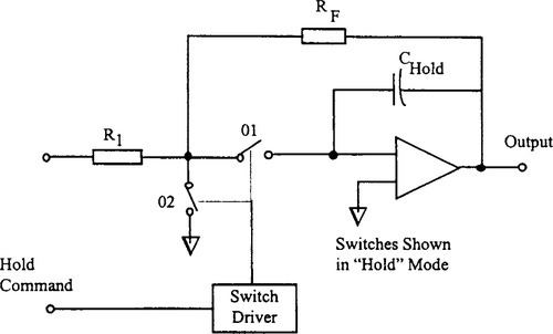
Switching from track to hold produces a transient, and the time required for the SHA output to settle to within a specified error band is called the hold mode settling time. Occasionally, the peak amplitude of the switching transient also is specified (see Figure 3-14).
3.4.1.3 Aperture and Aperture Time
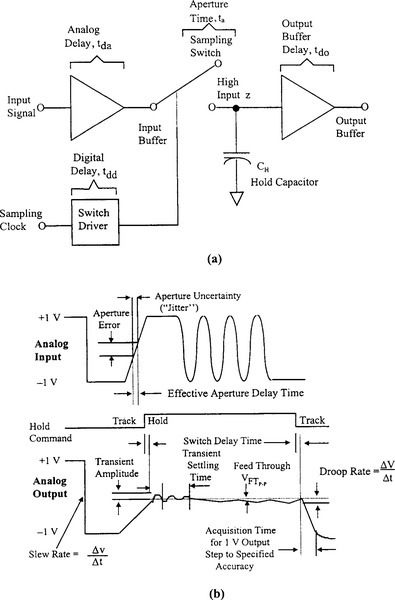
Perhaps the most misunderstood and misused SHA specifications are those that include the word aperture. The most essential dynamic property of an SHA is its ability to disconnect quickly the hold capacitor from the input buffer amplifier (see Figure 3-13(a)).
The short (but nonzero) interval required for this action is called the aperture time (ta). The actual value of the voltage held at the end of this interval is a function of both the input signal and the errors introduced by the switching operation itself. Figure 3-15 shows what happens when the hold command is applied with an input signal of arbitrary slope (for clarity, the sample-to-hold pedestal and switching transients are ignored). The value finally held is a delayed version of the input signal, averaged over the aperture time of the switch, as shown in Figure 3-15. The first-order model assumes that the final value of voltage on the hold capacitor is approximately equal to the average value of the signal applied to the switch over the interval during which the switch changes from a low to a high impedance (ta).
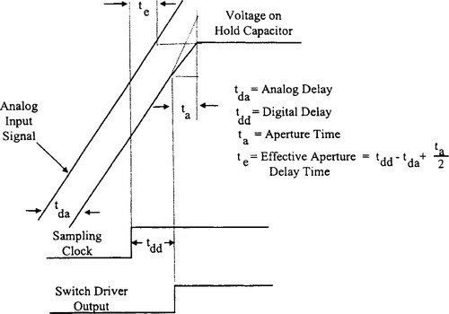
The model shows that the finite time required for the switch to open (ta) is equivalent to introducing a small delay in the sampling clock driving the SHA. This delay is constant and may be either positive or negative. Called effective aperture delay time or simply aperture delay (te), it is defined as the time difference between the analog propagation delay of the front-end buffer (tda) and the switch digital delay (tdd) plus half the aperture time (ta/2). The effective aperture delay time usually is positive but may be negative if the sum of half the aperture time (ta/2) and the switch digital delay (tdd) is less than the propagation delay through the input buffer (tda). The aperture delay specification thus establishes when the input signal actually is sampled with respect to the sampling clock edge.
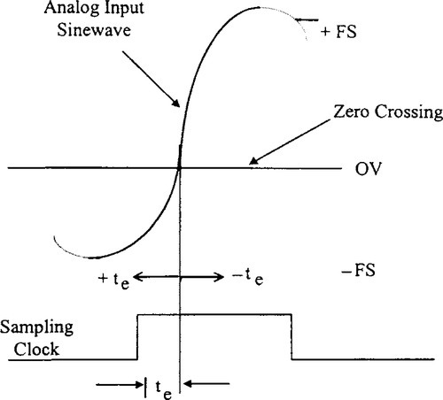
The aperture delay time can be measured by applying a bipolar sine wave signal to the SHA and adjusting the synchronous sampling clock delay such that the output of the SHA is 0 during the hold time. The relative delay between the input sampling clock edge and the actual zero crossing of the input sine wave is the aperture delay time (see Figure 3-16).
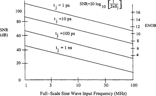
Aperture delay produces no errors but acts as a fixed delay in either the sampling clock input or the analog input (depending on its sign). If there is sample-to-sample variation in aperture delay (aperture jitter), then a corresponding voltage error is produced, as shown in Figure 3-17. This sample-to- sample variation in the instant that the switch opens, called aperture uncertainty or aperture jitter, usually is measured in rms picoseconds. The amplitude of the associated output error is related to the rate of change of the analog input. For any given value of aperture jitter, the aperture jitter error increases as the input dv/dt increases.

Measuring aperture jitter error in an SHA requires a jitter-free sampling clock and analog input signal source, because jitter (or phase noise) on either signal cannot be distinguished from the SHA aperture jitter itself—the effects are the same. In fact, the largest source of timing jitter errors in a system most often is external to the SHA (or the ADC if it is a sampling one), caused by noisy or unstable clocks, improper signal routing, and lack of attention to good grounding and decoupling techniques. SHA aperture jitter generally is less than 50 ps rms and less than 5 ps rms in high-speed devices.
Figure 3-18 shows the effects of total sampling clock jitter on the signal- to-noise ratio of a sampled data system. The total rms jitter will be composed of a number of components, the actual SHA aperture jitter often being the least of them.
3.4.1.4 Hold Mode Droop
During the hold mode, there are errors due to imperfections in the hold capacitor, switch, and output amplifier. If a leakage current flows in or out of the hold capacitor, it will slowly charge or discharge and its voltage will change, an effect known as droop in the SHA output, expressed in V/μs. Droop can be caused by leakage across a dirty PCB if an external capacitor is used or by a leaky capacitor but most commonly is due to leakage current in semiconductor switches and the bias current of the output buffer amplifier. An acceptable value of droop is found when the output of an SHA does not change by more than 1/2 LSB during the conversion time of the ADC it is driving. See Figure 3-19.

Droop can be reduced by increasing the value of the hold capacitor, but this will increase acquisition time and reduce the bandwidth in the track mode. Even quite small leakage currents can cause troublesome droop when SHAs use small hold capacitors. Leakage currents in PCBs may be minimized by the intelligent use of guard rings. Details of planning a guard ring are discussed in Analog Devices (1995, Chapter 8).
3.4.1.5 Dielectric Absorption
Hold capacitors for SHAs must have low leakage, but another characteristic is equally important: low dielectric absorption. If a capacitor is charged, discharged, and then left on an open circuit, it will recover some of its charge. The phenomenon, known as dielectric absorption, can seriously degrade the performance of an SHA, since it causes the remains of a previous sample to contaminate a new one and may introduce random errors of tens or even hundreds of millivolts (see Figure 3-20). After discharge, CD and RS in circuit could cause the residual charge.
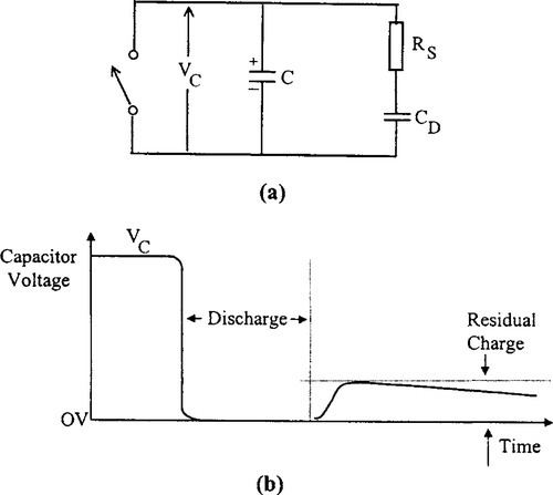
Different capacitor materials have differing amounts of dielectric absorption: electrolytic capacitors are dreadful (and their leakage is high) and some high- K ceramic types are bad, while mica, polystyrene, and polypropylene generally are good. Unfortunately, dielectric absorption varies from batch to batch, and even occasional batches of polystyrene and polypropylene capacitors may be affected. Measuring hold mode distortion is discussed in Analog Devices (1995, Chapter 8).
3.4.1.6 Hold-to-Track Transition Specification
When the SHA switches from hold to track, it must reacquire the input signal (which may have made a full-scale transition during the hold mode). Acquisition time is the interval of time required for the SHA to reacquire the signal to the desired accuracy when switching from hold to track. The interval starts at the 50% point of the sampling clock edge and ends when the SHA output voltage falls within the specified error band (usually 0.1% and 0.01% times are given). Some SHAs also specify acquisition time with respect to the voltage on the hold capacitor, neglecting the delay and settling time of the output buffer. The hold capacitor acquisition time specification is applicable in high-speed applications, where the maximum possible time must be allocated for the hold mode. The output buffer settling time, of course, must be significantly smaller than the hold time.
3.5 SHA Architectures
There are numerous SHA architectures and we will examine a few of the most popular ones. For a more detailed discussion on SHA architectures, see Razavi (1995).
3.5.1 Open-Loop Architecture
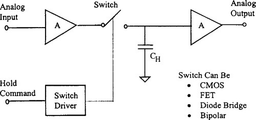
The simplest SHA architecture is shown in Figure 3-21. The input signal is buffered by an amplifier and applied to the switch. The input buffer may either be open or closed loop and may or may not provide gain. The switch can be CMOS, FET, or bipolar (using diodes or transistors), controlled by the switch driver circuit. The signal on the hold capacitor is buffered by an output amplifier. This architecture sometimes is referred to as open loop because the switch is not inside a feedback loop. Note that the entire signal voltage is applied to the switch; therefore, it must have excellent common mode characteristics.
3.5.2 Open-Loop Diode Bridge SHA
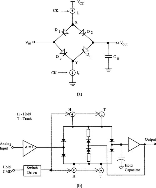
Semiconductor diodes exhibit small on-resistance, large off-resistance, high-speed switching, and thus potential for the switching function in sampling circuits. A simplified diagram of a typical diode switch is shown in Figure 3-22(a). Here, four diodes form a bridge that provides a low-impedance path from Vin to Vout when current sources I1 and I2 are on and (in the ideal case) isolates Vout from Vin when I1 and I2 are off. Nominally, I1 = I2 = I. Implementation is shown in Figure 3-22(b).
3.5.3 Closed-Loop Architecture
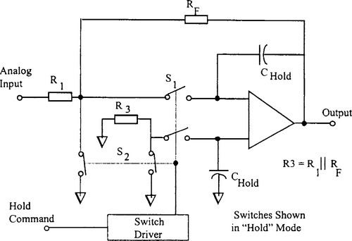
The SHA circuit shown in Figure 3-23 represents a classical closed-loop design and is used in many CMOS sampling ADCs. Since the switches always operate at virtual ground, there is no common mode signal across them. Switch S2 is required to maintain a constant input impedance and prevent the input signal from coupling to the output during the hold time. In the track mode, the transfer characteristic of the SHA is determined by the op amp and the switches introduce no DC errors because they are within the feedback loop. The effects of charge injection can be minimized by using the differential switching techniques shown in Figure 3-24.
3.6 ADC Architectures
Within the 1990s and the latter part of the 1980s, many architectures for A/D conversion have been implemented in monolithic form. Manufacturing process improvements achieved by mixed-signal product manufacturers have led to this unprecedented development, which was fueled by the demand from the product and system designers.
The most common ADC architectures in monolithic form are successive approximation, flash, integrating, pipeline, half flash (or subranging), two step, interpolative and folding, and sigma-delta (Σ-Δ). The following sections provide the basic operational and design details of these techniques.
While the Σ-Δ, successive approximation, and integrating types could give very high resolution at lower speeds, flash architecture is the fastest but with high power consumption. However, recent architecture breakthroughs have allowed designers to achieve a higher conversion rate at low power consumption with integral track and hold circuitry on a chip (McGoldrick, 1997). The AD9054 from Analog Devices is an example.
3.6.1 Successive Approximation ADCs
The successive approximation register (SAR) ADC architecture has been used for decades and still is a popular and cost effective form of converter for sampling frequencies up to few MSPS. A simplified block diagram of an SAR ADC is shown in Figure 3-25. On the start conversion command, all the bits of the successive approximation register are reset to 0 except the most significant bit (MSB), which is set to 1. Bit 1 is tested in the following manner. If the ADC output is greater than the analog input, the MSB is reset; otherwise, it is left set. The next most significant bit then is tested by setting it to 1. If the digital/analog converter (DAC) output is greater than the analog input, this bit is reset; otherwise it is left set. The process is repeated with each bit in turn. When all the bits have been set, tested, and reset or not as appropriate, the contents of the SAR correspond to the digital value of the analog input, and the conversion is complete.
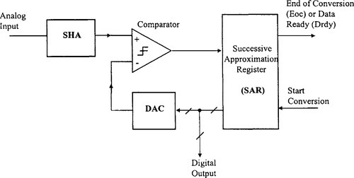
An N-bit conversion takes N steps. On superficial examination, a 16-bit converter would seem to have a conversion time twice as long as an 8-bit one, but this is not the case. In an 8-bit converter, the DAC must settle to 8-bit accuracy before the bit decision is made, whereas in a 16-bit converter, it must settle to 16-bit accuracy, which takes a lot longer. In practice, 8-bit successive approximation ADCs can convert in a few hundred nanoseconds, while 16-bit ones generally take several microseconds.
The classic SAR ADC is only a quantizer — no sampling takes place — and for an accurate conversion, the input must remain constant for the entire conversion period. Most modern SAR ADCs are sampling types and have internal sample and hold so that they can process AC signals. They are specified for both AC and DC applications. An SHA is required in an SAR ADC because the signal must remain constant during the entire N-bit conversion cycle.
The accuracy of an SAR ADC depends primarily on the accuracy (differential and integral linearity, gain, and offset) of the internal DAC. Until recently, this accuracy was achieved using laser-trimmed thin-film resistors. Modern SAR ADCs utilize CMOS switched capacitor charge redistribution DACs. This type of DAC depends on the accurate ratio matching and the stability of on-chip capacitors rather than thin-film resistors. For resolutions greater than 12 bits, on-chip autocalibration techniques, using an additional calibration DAC and the accompanying logic, can accomplish the same thing as thin-film laser-trimmed resistors, at much less cost. Therefore, the entire ADC can be made on a standard submicròn CMOS process.
The successive approximation ADC has a very simple structure, low power, and reasonably fast conversion times (< 1 MSPS). It is probably most widely used ADC architecture and will continue to be used for medium-speed, mediumresolution applications.
Current 12-bit SAR ADCs achieve sampling rates up to about 1 MSPS, and 16-bit ones up to about 300 kSPS. Examples of typical state of the art SAR ADCs are the AD7892 (12 bits at 600 kSPS), the AD976/977 (16 bits at 100 kSPS), and the AD7882 (16 bits at 300 kSPS).
3.6.2 Flash Converter
Flash ADCs (sometimes called parallel ADCs) are the fastest ADCs and use large numbers of comparators. An N-bit flash ADC consists of 2N resistors and 2N— 1 comparators arranged as in Figure 3-26. Each comparator has a reference voltage 1 least significant bit (LSB) higher than that of the one below it in the chain. For a given input voltage, all the comparators below a certain point will have their input voltage larger than their reference voltage and a 1 logic output, and all the comparators above that point will have a reference voltage larger than the input voltage and a 0 logic output. The 2N — 1 comparator output therefore behaves like a mercury thermometer, and the output code at this point is sometimes called a thermometer code. Since 2N — 1 data output is not really practical, these are processed by a decoder to an N-bit binary output.
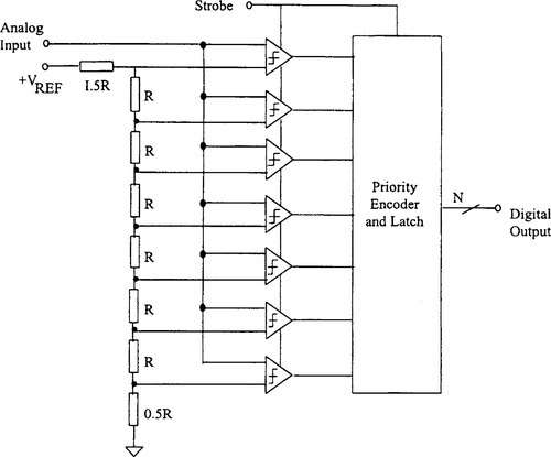
The input signal is applied to all the comparators at once, so the thermometer output is delayed by only one comparator delay from the input and the encoder N-bit output by only a few gate delays on top of that, so the process is very fast. However, the architecture uses large numbers of resistors and comparators and is limited to low resolutions; if it is to be fast, each comparator must run at relatively high power levels. Hence, the problems of flash ADCs include limited resolution, high power dissipation because of the large number of high-speed comparators (especially at sampling rates greater than 50 MSPS), and relatively large (and therefore expensive) chip sizes. In addition, the resistance of the reference resistor chain must be kept low to supply adequate bias current to the fast comparators, so the voltage reference has to source quite large currents (> 10 mA).
In practice, flash converters are available up to 10 bits of resolution, but more commonly they have 8 bits of resolution. Their maximum sampling rate can be as high as 500 MSPS, and input full-power bandwidths are in excess of 300 MHz.
But, as mentioned earlier, full-power bandwidths are not necessarily full-resolution bandwidths. Ideally, the comparators in a flash converter are well matched both for DC and AC characteristics. Because the strobe is applied to all the comparators simultaneously, the flash converter is inherently a sampling converter. In practice, delay variations between the comparators and other AC mismatches cause a degradation in ENOB at high input frequencies. This is because the inputs are slewing at a rate comparable to the comparator conversion time.
The input to a flash ADC is applied in parallel to a large number of comparators. Each has a voltage-variable junction capacitance, and this signal-dependent capacitance results in all flash ADCs having reduced ENOB and higher distortion at high input frequencies. For more details, see Analog Devices (1996).
3.6.3 Integrating ADCs
The integrating ADC is a very popular architecture in applications where a very slow conversion rate is acceptable. A classic example is the digital multimeter.
All the converters discussed so far can digitize analog inputs at speeds of at least 10 kSPS. A typical integrating converter is slow relative to these high-speed converters. Useful for precisely measuring slowly varying signals, the integrating converter finds applications in low-frequency and DC measurement applications.
Integrating converters are based on an indirect conversion method. Here the analog input voltage is converted to a time period and later to a digital number using a counter. The integration eliminates the need for a sample/hold (S/H) circuit to “capture” the input signal during the measurement period. The two common variations of the integrating converter are the dual slope type and the charge balance or multislope type. The dual slope technique is very popular among instrument manufacturers because of its simplicity, low price, and better noise rejection. The multislope technique is an improvement on the dual slope method.
Figure 3-27(a) shows a typical integrating converter. It consists of an analog integrator, a comparator, a counter, a clock, and control logic. Figure 3-27(b) shows the circuit’s charge (T1) and discharge (T2) waveforms. The conversion is started by closing the switch and thereby connecting the capacitor, Cint, to the unknown input voltage, Vin, through the resistor, R. This results in a linear ramp at the integrator output for a fixed period, T1 controlled by the counter. The control circuit then switches the integrator input to the known reference voltage, Vref, and the capacitor discharges until the comparator detects that the integrator has reached the original starting point. The counter measures the amount of time taken for the capacitor to discharge.

Because the values of the resistor, the integrating capacitor, and the frequency of the clock remain the same for both the charge and discharge cycles, the ratio of the charge time to the discharge time is equal to the ratio of the reference voltage to the unknown input voltage. The absolute values of the resistor, capacitor, and the clock frequency therefore do not affect the conversion accuracy. Furthermore, any noise on the input signal is integrated over the entire sampling period, which imparts a high level of noise rejection to the converter. By making the signal integration period an integral multiple of the line frequency period, the user can obtain excellent line frequency noise rejection.
A charge balance integrating converter incorporates many of the elements of the dual slope converter but uses a free-running integrator in a feedback loop. The converter continuously attempts to null its input by subtracting precise charge packets when the accumulated charge exceeds a reference value. The frequency of the charge packets (the number of packets per second) the converter needs to balance the input is proportional to that input. Clock-controlled synchronous logic delivers a serial output that a counter converts to a digital word in the circuit. Integrating converters in monolithic form typically are used in digital voltmeters due to their high resolution properties. Hybrid integrating converters with 22- bit resolutions were introduced to the market in the late 1980s. It therefore is possible to expect higher resolutions in the monolithic market as well. There could be many variations of this technique as applied to digital multimeters, and Kularatna (1996) is suggested for details.
3.6.4 Pipeline Architectures
The concept of a pipeline, often used in digital circuits, can be applied in the analog domain to achieve higher speed where several operations must be performed serially. Figure 3-28 shows a general (analog or digital) pipeline system. Here, each stage carries out an operation on a sample, provides the output for the following sampler, and once that sampler has acquired the data, begins the same operation on the next sample. Thus, at any given time, all the stages are processing different samples concurrently; hence, the throughput rate depends only on the speed of each stage and the acquisition time of the next sampler.

To arrive at a simple example of an analog pipeline, consider a two-step ADC, where four operations (coarse A/D conversion, interstage D/A conversion, subtraction, and fine A/D conversion) must be performed serially. As such, the ADC cannot begin to process the next sample until all four operations are finished. Now, suppose an SHA is interposed between the subtractor and the fine stage, as shown in Figure 3-29, so that the residue is stored before fine conversion begins. Thus, the front-end SHA, the coarse ADC, the interstage DAC, and the subtractor can start processing the next sample while the fine ADC operates on the previous one, allowing potentially faster conversion. More details on pipeline architectures can be found in Louzon (1995).
3.6.5 Half-Flash ADCs
Although it is not practical to make them with high resolution, flash ADCs often are used as subsystems in “subranging” ADCs (sometimes known as half-flash ADCs), which are capable of much higher resolutions (up to 16 bits).
A block diagram of an 8-bit subranging ADC based on two 4-bit flash converters is shown in Figure 3-30. Although 8-bit flash converters are readily available at high sampling rates, this sample will be used to illustrate the theory. The conversion process is done in two steps. The four most significant bits are digitized by the first flash (to better than 8-bit accuracy) and the 4-bit binary output is applied to 4-bit DAC (again, better than 8-bit accuracy). The DAC output is subtracted from the held analog input, and the resulting residue signal is amplified and applied to the second 4-bit flash. The output of the two flash converters are combined into a single 8-bit binary output word. If the residue signal range does not exactly fill the range of the second flash converter, nonlinearities and perhaps missing codes1 will result.

Modern subranging ADCs use a technique called digital correction to eliminate problems associated with the architecture of Figure 3-30. A simplified block diagram of a 12-bit digitally corrected subranging ADC is shown in Figure 3-31. An example of such a practical ADC is the AD9042 from Analog Devices, a 12-bit, 41 MSPS device. Key specifications of the AD9042 are given in Table 3-3.
Table 3-3
Key Specifications of the AD9042.
| Parameter | Value |
| Input range | 1 V peak-to-peak, Vcm = + 2.4 V |
| Input impedance | 250 Ω to Vcm |
| Effective input noise | 0.33 LSBs rms |
| SFDR at 20 MHz input | 80 dB minimum |
| SINAD (S/N + D) at 20 MHz input | 67 dB |
| Digital outputs | TTL compatible |
| Power supply | Single + 5 V |
| Power dissipation | 595 mW |
| Fabrication | High-speed dielectrically isolated complementary bipolar process |
(Reproduced by permission of Analog Devices Inc.)
Note that a 6-bit and 7-bit ADC have been used to achieve an overall 12-bit output. These are not flash ADCs but utilize a magnitude-amplifier (MagAmp™) architecture. (See Chapter 4 in Analog Devices (1996) for MagAmp™ basics.) If there were no errors in the first-stage conversion, the 6-bit “residue” signal applied to the 7-bit ADC by the summing amplifier would never exceed one- half the range of the 7-bit ADC. The extra range in the second ADC is used in conjunction with the error correction logic (usually just a full adder) to correct the output data for most of the errors inherent in the traditional uncorrected subranging converter architecture. It is important to note that the 6-bit DAC must be better than 12-bit accurate, because the digital error correction does not correct for DAC errors. In practice, “thermometer” or “fully decoded” DACs using one current switch per level (63 switches in the case of a 6-bit DAC) often are used instead of a “binary” DAC to ensure excellent differential and integral linearity and minimum switching transients (Analog Devices, 1996).
The second SHA delays the held output of the first SHA while the first-stage conversion occurs, thereby maximizing throughput. The third SHA “deglitches” the residue output signal, allowing a full conversion cycle for the 7-bit ADC to make its decision (the 6- and 7-bit ADCs in the AD9042 are bit-serial MagAmp ADCs, which require more settling time than a flash converter). Additional shift registers in series with the digital output of the first-stage ADC ensure that its output ultimately is time-aligned with the last 7 bits from the second ADC when their outputs are combined in the error correction logic. A pipeline ADC therefore has a specified number of clock cycles of latency — pipeline delay — associated with the output data. The leading edge of the sampling clock (for sample, N) is used to clock the output register, but the data that appears as a result of that clock edge corresponds to sample N — L, where L is the number of clock cycles of latency; in the case of the AD9042, two clock cycles of latency.
The error correction scheme described previously is designed to correct for errors made in the first conversion. Internal ADC gain, offset, and linearity errors are corrected as long as the residue signal falls within the range of the second- stage ADC. These errors will not affect the linearity of the overall ADC transfer characteristic. Errors made in the final conversion, however, translate directly as errors in the overall transfer function. Also, linearity errors or gain errors either in the DAC or the residue amplifier will not be corrected and will show up as nonlinearities or nonmonotonic behavior in the overall ADC transfer function.
So far, we have considered only two-stage subranging ADCs, as these are easiest to analyze. There is no reason to stop at two stages, however. Three-pass and four-pass subranging pipeline ADCs are quite common and can be made in many different ways, usually with digital error correction. For details, see Analog Devices (1996).
3.6.6 Two-Step Architectures
The exponential growth of power, die area, and input capacitance of flash converters as a function of resolution makes them impractical for resolutions above 8 bits in general. These resolutions call for topologies that provide a more relaxed trade-off among the parameters. Two-step architectures trade speed for power, area, and input capacitance.
In a two-step ADC, first a coarse analog estimate of the input is obtained to yield a small voltage range around the input level. Subsequently, the input level is determined with higher precision within this range. Figure 3-32(a) illustrates a two-step architecture consisting of a front-end SHA, a coarse flash ADC stage, a DAC, a subtractor, and a fine flash ADC stage. We describe its operation using the timing diagram shown in the Figure 3-32(b).
For t < t1 the SHA tracks the analog input. At t = t1, the SHA enters a hold mode and the first flash stage is strobed to perform the coarse conversion. The first stage then provides a digital estimate of the signal held by the SHA (VA), and the DAC converts this estimate to an analog signal (VB), which is a coarse approximation of the SHA output. Next, the subtractor generates an output equal to the difference between VA and VB (VC, called the residue), which is subsequently digitized by the fine ADC. Comparison of timing in flash and two- step architectures is shown in Figure 3-32(c). For more details, see Razavi (1996).
A two-step ADC need not employ two separate flash stages to perform the coarse and fine conversions. One stage can be used for both; and such an architecture, shown in Figure 3-33, is called recycling architecture.
Here, during the coarse conversion, the flash stage senses the front-end SHA output, VA, and generates the coarse digital output. This digital output then is converted to analog by the DAC and subtracted from VA by the subtractor. During fine conversion, the subtractor output is digitized by the flash stage. Note that, in this phase, the ADC full-scale voltage must be equal to that of the subtractor output. Therefore, for proper fine conversion, either the ADC reference voltage must be reduced or the residue must be amplified.
While reducing area and power dissipation by roughly a factor of 2 relative to two-stage ADCs, recycling converters suffer from other limitations. The converter must now employ either low-offset comparators (if the subtractor has a gain of 1), inevitably slowing down the coarse conversion, or a high-gain subtractor, increasing the interstage delay. This is in contrast with two-stage ADCs, where the coarse stage comparators need not have a high resolution and hence can operate faster.
3.6.7 Interpolating and Folding Architectures
To maintain the one-step nature of the flash-type architectures, without adding sample-and-hold circuits to the ADC, several other architectures are available. Among these techniques, interpolation and folding have proven quite beneficial. Earlier, these techniques had been applied predominantly to bipolar circuits; recently CMOS devices have entered the market.
As a comprehensive discussion on these techniques is beyond the scope of this chapter, only basic approach in the design is discussed here.
3.6.7.1 Interpolating Architectures
To reduce the number of preamplifiers at the input of a flash ADC, the difference between the analog input and each reference voltage can be quantized at the output of each preamplifier. This is possible because of the finite gain — hence, nonzero linear input range — of typical preamplifiers used as the front end of comparators.
We illustrate this concept in Figure 3-34(a). In Figure 3-34(a), preamplifiers A1 and A2 compare the analog input with Vr1 and Vr2, respectively. In Figure 3-34(b), the input/output characteristics of A1 and A2 are shown. Assuming zero offset for both preamplifiers, we note that VX1 = VY1 if Vin = Vr1 and VX2 = VY2 if Vin = Vr2. More important, VX2 = VY1 if Vin = Vm = (Vr1+ Vr2)/2; that is, the polarity of the difference between VX2 and VY1is the same as that of the difference between Vin and Vm.
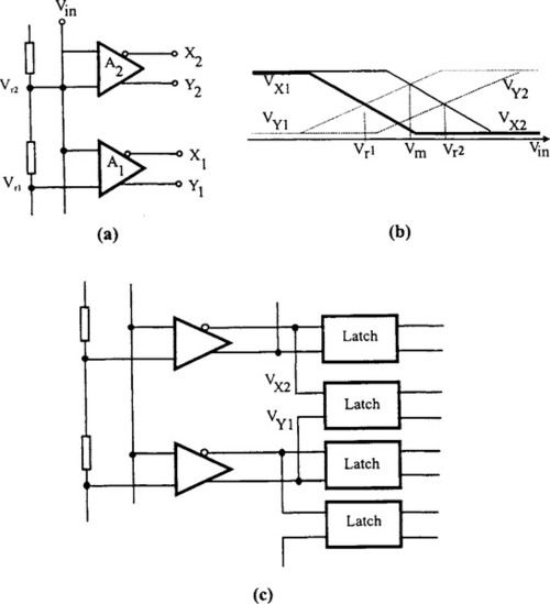
The preceding observation indicates that the equivalent resolution of a flash stage can be increased by “interpolating” between the output of preamplifiers. For example, Figure 3-34(c) shows how an additional latch detects the polarity of the difference between the single-ended output of two adjacent preamplifiers. Note that in contrast with a simple flash stage, this approach halves the number of preamplifiers but maintains the same number of latches.
The interpolation technique of Figure 3-34(c) substantially reduces the input capacitance, power dissipation, and area of flash converters, while preserving the one-step nature of the architecture. This is possible because all the signals arrive at the input of the latches simultaneously and hence can be captured on one clock edge. Since this configuration doubles the effective resolution, we say it has an interpolation factor of 2. For further details on this architecture, see Razavi (1996).
3.6.7.2 Folding Architectures
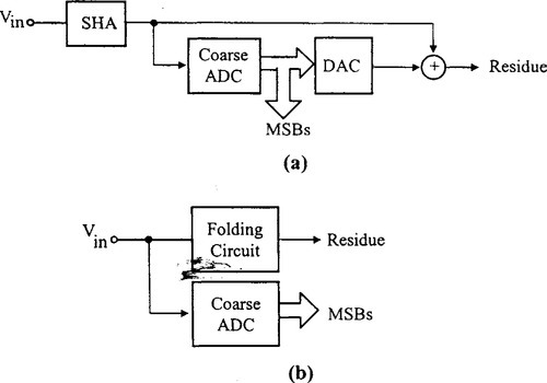
Folding architectures have evolved from flash and two-step topologies. Folding architectures perform analog preprocessing to reduce hardware while maintaining the one-step nature of flash architectures.
The basic principle in folding is to generate a residue voltage through analog preprocessing and subsequently digitize that residue to obtain the least significant bits. The most significant bits can be resolved using a coarse flash stage that operates in parallel with the folding circuit and, hence, samples the signal at approximately the same time that the residue is sampled. Figure 3-35 depicts the generation of residue in two-step and folding architectures. In a two-step architecture, coarse A/D conversion, interstage D/A conversion, and subtraction must be completed before the proper residue becomes available. In contrast, folding architectures generate the residue “on the fly” using simple wideband stages.
To illustrate this principle, we first describe a simple, ideal approach to folding. Consider two amplifiers, A1 and A2, with the input/output characteristics depicted in Figure 3-36(a). The active region of one amplifier is centered around (Vr2 + Vr1)/2 and that of the other around (Vr3 + Vr2)/2, and Vr3 – Vr2 = Vr2— Vr1. Each amplifier has a gain of 1 in the active region and 0 in the saturation region. If the outputs of the two amplifiers are summed, the “folding” characteristic of Figure 3-36(b) results, yielding an output equal to Vin – Vrl for Vr1 < Vin < Vr2 and (–Vin + V r2 + Δ) for Vr2 < Vin < Vr3, where Δ is the value of the summed characteristics at Vin = Vr2. If Vr1, Vr2, and Vr3 are the reference voltages in an ADC, then these two regions can be viewed as the residue characteristics of the ADC for Vr1 < Vin < Vr3 To understand why, we compare this characteristic with that of a two-step architecture, as shown in Figure 3-36(c). The two characteristics are similar except for a negative sign and a vertical shift in the folding output for Vr2 < Vin < Vr3. Therefore, if the system accounts for the sign reversal and level shift, the folding output can be used as the residue for fine digitization.
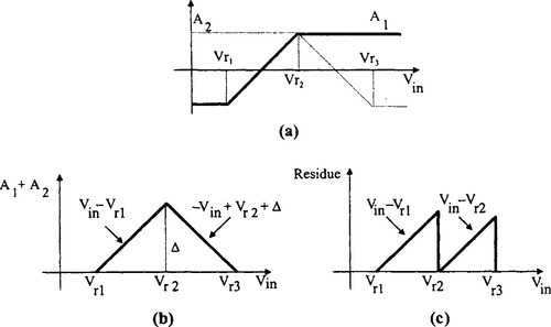
Figure 3-37(a) shows an implementation of folding. Here, four differential pairs process the difference between Vin and Vr1,…, Vr4, and their output currents are summed at nodes X and Y. Note that the outputs of adjacent stages are added with opposite polarity; for example, as Vin increases, Q1 pulls node X low while Q2 pulls node Y low. Current source I5 shifts VY down by IR. To explain the operation of the circuit, we consider its input/output characteristics, plotted in Figure 3-37(b). For Vin well below Vr1, Q1 – Q4 are off, Q5 – Q8 are on. I2 and I4 flow through Rc1, and I1,I3, and I5 flow through Rc2- As Vin exceeds Vmax by several VT, Q5 turns off, allowing VX and VY to reach Vmin and Vmax, respectively. As Vin approaches Vr2, Q2 begins to turn on and the circuit behaves as before. Considering the differential output, VX – VY, we note that the resulting characteristic exhibits folding points at (Vr1 + Vr2)/2, (Vr2 + Vr3)/2, and so forth. As Vin goes from below Vr1to above Vr4, the slope of VX – VY changes sign four times; hence, we say the circuit has a folding factor of 4.

The simplicity and speed of folding circuits have made them quite popular in A/D converters, particularly because they eliminate the need for sample-and- hold amplifiers, D/A converters, and subtractors. Nevertheless, several drawbacks limit their use at higher resolutions (Razavi, 1995).
3.6.8 Sigma-Delta Converters
Sigma-Delta analog/digital converters (Σ-Δ ADCs) have been known for nearly 30 years, but only recently has the technology (high-density digital very large-scale ICs) existed to manufacture them as inexpensive monolithic integrated circuits. They are used in many applications where a low-cost, low-bandwidth, high-resolution ADC is required.
The literature contains innumerable descriptions of the architecture and theory of Σ-Δ ADCs (Candy and Temes, 1992). As a text of this nature is not appropriate for describing their mathematical analysis and background, this section has been written to classify the subject. A practical monolithic Σ-Δ ADC contains very simple analog circuit blocks (a comparator, a switch, and one or more integrators and analog summing circuits) and quite complex digital computational circuitry. The circuitry consists of a digital signal processor that acts as a filter (generally, but not invariably, a low-pass filter). It is not necessary to know how the filter works to appreciate what it does. To understand how a Σ-Δ ADC works, one should be familiar with the concepts of oversampling, noise shaping, digital filtering, and decimation. We briefly discuss these concepts in Σ-Δ converters.
3.6.8.1 Key Concepts Behind the Σ-Δ ADC
Figure 3-38 shows the transfer characteristic of a 3-bit unipolar Σ-Δ ADC. The input to an ADC is analog and is not quantized, but its output is quantized. The transfer characteristic therefore consists of eight horizontal steps (when considering the offset, gain, and linearity of an ADC, we consider the line joining the midpoints of these steps). Digital full scale (all ones) corresponds to 1 LSB below the analog full scale (the reference or some multiple of it). This is because, as mentioned previously, the digital code represents the normalized ratio of the analog signal to the reference, and if this were unity, the digital code would be all zeros and 1 in the bit above the MSB.
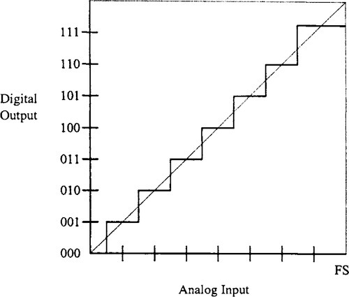
The (ideal) ADC transitions take place at 0.5 LSB above 0 and thereafter every LSB, up to 1.5 LSB below analog full scale. Since the analog input to an ADC can take any value but the digital output is quantized, there may be a difference of up to 0.5 LSB between the actual analog input and the exact value of the digital output. This is known as the quantization error or quantization uncertainty. In AC (sampling) applications, this quantization error gives rise to quantization noise. If we apply a fixed input to an ideal ADC, we always will obtain the same output and the resolution will be limited by the quantization error.
Suppose, however, that we add some AC (dither) to the fixed signal, take a large number of samples, and prepare a histogram of the results. We will obtain something like the result in Figure 3-39. If we calculate the mean value of a large number of samples, we will find that we can measure the fixed signal with greater resolution than that of the ADC we are using. This procedure is known as oversampling.

The AC (dither) that we add may be a sine wave, a triangular wave, or Gaussian noise (but not a square wave); and with some types of sampling ADCs (including Σ-Δ ADCs), an external dither signal is unnecessary, since the ADC generates its own. Analysis of the effects of differing dither waveforms and amplitudes is complex and, for the purposes of this section, unnecessary. What we need to know is that with the simple oversampling described here, the number of samples must be doubled for each bit of increase in resolution.
If, instead of a fixed DC signal, the signal that we are oversampling is AC, then it is not necessary to add a dither signal to it to oversample, since the signal is moving anyway. (If the AC signal is a single-tone, harmonically related to the sampling frequency, dither may be necessary, but this is a special case.)
Consider the technique of oversampling with an analysis in the frequency domain. Where a DC conversion has a quantization error of up to 1/2 LSB, a sampled data system has quantization noise. As we already have seen, a perfect classical TV-bit sampling ADC has an rms quantization noise of ![]() uniformly distributed within the Nyquist band of DC to fs/2 (where q is the value of an LSB and fs is the sampling rate), giving us an SNR of (6.02N + 1.76) dB with full-scale sine wave inputs (e.g., equation (3.1); see Figure 3-40).
uniformly distributed within the Nyquist band of DC to fs/2 (where q is the value of an LSB and fs is the sampling rate), giving us an SNR of (6.02N + 1.76) dB with full-scale sine wave inputs (e.g., equation (3.1); see Figure 3-40).

If the ADC is less than perfect and its noise is greater than its theoretical minimum quantization noise, then its effective resolution will be less than N bits. Its actual resolution (often known as its effective number of bits, ENOB) will be defined by equation (3.2).
If we choose a much higher sampling rate (K times fs, as in Figure 3-41(a)), the quantization noise is distributed over a wider bandwidth as shown in Figure 3-41 (b). If we then apply a digital low-pass filter to the output, we remove much of the quantization noise but do not affect the wanted signal, so the ENOB is improved. We have performed a high-resolution A/D conversion with a low resolution ADC.
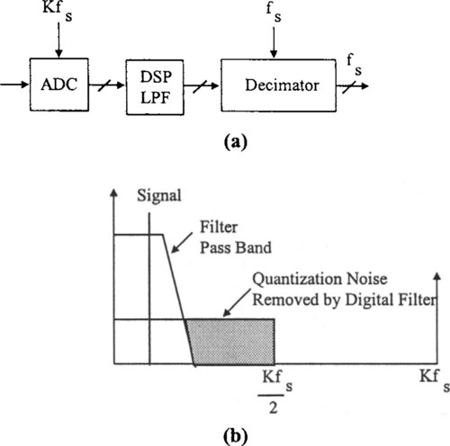
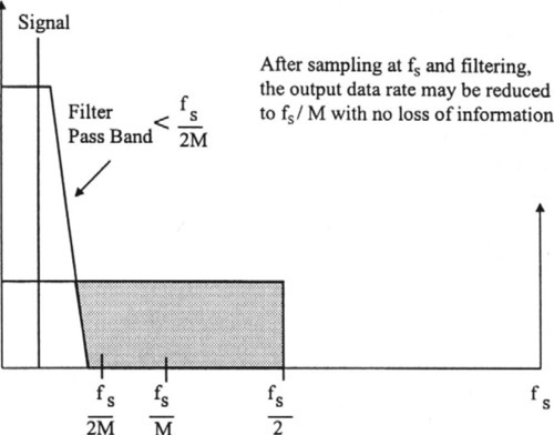
Since the bandwidth is reduced by the digital output filter, the output data rate may be lower than the original sampling rate and still satisfy the Nyquist criteria. This may be achieved by passing every M th result to the output and discarding the remainder, a process is known as decimation by a factor of M. Here, M can have any integer value, provided that the output data rate is more than twice the signal bandwidth. Decimation causes no loss of information (Figure 3-42). As shown in Figure 3-42, after sampling at fs and filtering, the output data rate may be reduced to fs/M with no loss of information.
3.6.8.2 Block Diagram of a Σ-Δ ADC
Oversampled Σ-Δ ADCs in recent years have become more prevalent for high-accuracy, 12 bit to beyond 22 bit, A/D conversion of DC through moderately high (hundreds of kHz) AC signals. Their greatest advantage is that they trade greatly reduced analog circuit accuracy requirements for increased digital circuit complexity. This is a distinct advantage for 1 -2 micron and submicron very large-scale integrated (VLSI) digital circuit technologies. VLSI circuit techniques can achieve circuit densities of hundreds of thousands of gates, allowing complex digital filters to be integrated on the chip. The result is high precision at low cost.
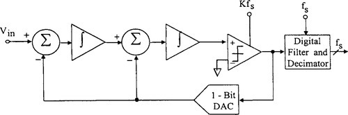
The basic oversampled Σ-Δ A/D converter (Figure 3-43) is an integrating A/D converter. The single-bit feedback D/A converter output is subtracted from the analog input signal, Vin, in the summing amplifier. The resulting error signal from the summing amplifier output is low-pass filtered by the integrator and thé integrated error signal polarity is detected by the single comparator. This comparator effectively is a 1-bit A/D converter.
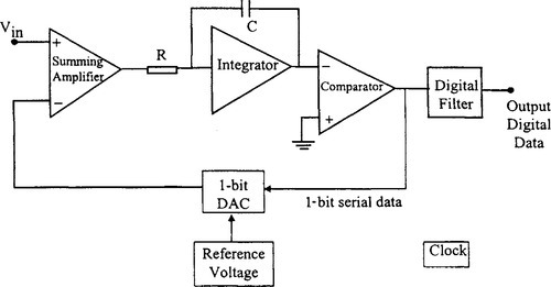
The output of the comparator drives the 1-bit DAC to a 1 or 0 (a 1, if during the previous sample time the integrator output was detected by the comparator as being too low, that is, below 0 V; a 0, if the difference detected during the previous sample was too high, that is, above 0 V reference of the comparator).
The 1-bit D/A converter, as in successive approximation A/D converters, provides the negative feedback. This negative feedback for a 1 in the D/A converter always is in a direction to drive the integrator output toward 0 V. The D/A converter output for a 1 input would be the reference voltage. The reference voltage would be equal to or exceed the expected full-scale analog input signal voltage. Then, for a small value of Vin, the integrator would take many clock pulses to cross 0 V, after a single 1 was generated, during which time the comparator is sending zeros to the digital filter. If Vin were at full scale, the integrator would cross 0 every clock time and the comparator output would be a string of alternate ones and zeros. The digital filter’s function is to determine a digital number at its output that is proportional to the number of ones in the previous bit stream from the comparator. Various types of digital filters are used to perform this computational function, which is the most complex function in this type of D/A converter. However, complex digital computations can be performed readily in a VLSI circuit.
Oversampled converters sample at much higher rates than the Nyquist rate. The oversampling ratio is equal to the actual sampling rate divided by the Nyquist rate. The oversampling rate can be hundreds to thousands of times the analog input signal frequency bandwidth. Since each sample is in a 1-bit low accuracy conversion, sampling rates can be very high.
In cases where antialiasing filtering is required on the input analog signal, the filter does not require the sharp cutoff characteristics as would be required to limit broadband signals prior to a successive approximation-type A/D converter operating at or near a small multiple of the Nyquist sampling rate. The reason is that the oversampling rate is many times the Nyquist rate. Therefore, a simple RC filter is adequate to prevent aliasing. The input filter can pass frequencies many times higher than the frequencies of interests before filter cutoff is required. The bandwidth of signals converted can be increased significantly by a sigma-delta A/D converter at a given clock sampling rate by using a multibit A/D and D/A converter rather than a single-bit A/D and D/A converter. Digital filter design is another variable affecting the bandwidth of signals that can be accurately converted for a given oversampling rate.
However, the greatest advantage of an oversampled Σ-Δ converter is that it requires only a single-bit A/D and D/A converter with a relatively inaccurate differential summing amplifier and integrator (low-pass filter). These analog circuits are much easier to implement in a digital VLSI circuit than the accurate analog circuits required in parallel- and successive-approximation A/D converters that require precision resistors or capacitors. This is especially true when accuracies exceed 12 bits.
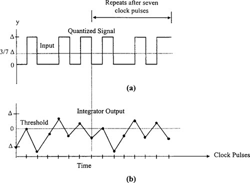
Based on the preceding description, we can show that the quantized signal bounces between two levels, keeping its mean equal to the input, when the input to the modulator is a DC signal. Figure 3-44 shows the quantized signal and the integrated output when the input signal is 3Δ/7 above 0 for a quantization level of Δ. The figure indicates that the oscillation may be repetitive (it returns to its starting condition after seven clock periods). The frequency of repetition depends on the input level.
By using more than one integration and summing stage in the Σ-Δ modulator, higher orders of quantization noise shaping and better ENOB for a given oversampling ratio can be achieved (Analog Devices, 1995). A block diagram of a second order Σ-Δ ADC is shown in Figure 3-45.
3.6.9 Self-Calibration Techniques
Integral linearity of data converters usually depends on the matching and linearity of integrated resistors, capacitors, or current sources; and it is typically limited to approximately 10 bits with no calibration. For higher resolutions, means must be sought that can reliably correct nonlinearity errors. This often is accomplished by either improving the effective matching of individual devices or correcting the overall transfer characteristics. Since high-resolution A/D converters typically employ a multistep architecture, they often impose two stringent requirements: small integral nonlinearity in their interstage DACs and precise gain (usually a power of 2) in their interstage subtractors/amplifiers. These constraints in turn demand correction for device mismatches if resolutions above 10 bits are required.
ADC calibration techniques can be in two forms: use of analog processing techniques for correction of nonidealities and digital calibration techniques. A description of these techniques is beyond the scope of this chapter. For details, see Razavi (1995), Kularatna (1996), and O’Leary (1995).
3.6.10 Figure of Merit for ADCs
The demand for lower power-dissipating electronic systems has become a challenge to the IC designer, including designers of ADCs. As a result, a figure of merit was devised by the ISSCC1 Program Committee to compare available and future sampling-type ADCs. The figure of merit (FOM) is based on an ADC’s power dissipation, its resolution, and its sampling rate. The FOM is derived by dividing the device’s power dissipation (in watts) by the product of its resolution (in 2n bits) and its sampling rate (in hertz). The result is multiplied by 1012. This is expressed by the equation
where
PD = Power dissipation (in watts);
R = Resolution (in 2n bits);
SR = Sampling rate (in hertz).
Therefore, a 12-bit ADC sampling at 1 MHz and dissipating 10 mW has a figure of merit rounded off to 2.5. This figure of merit is expressed in the units of picojoules of energy per unit conversion (pj)/conversion. For details and a comparison of performance of some monolithic ICs, see Goodenough (1995).
3.7 D/A Converters
Digital-to-analog conversion is an essential function in data processing systems. D/A converters provide an interface between the digital output of signal processes and the analog world. Moreover, as discussed previously, multistep ADCs employ interstage DACs to reconstruct analog estimates of the input signal. Each of these applications imposes certain speed, precision, and power dissipation requirements on the DAC, mandating a good understanding of various D/A conversion techniques and their trade-offs.
3.7.1 General Considerations
A digital-to-analog converter produces an analog output, A, proportional to the digital input D:
where α is a proportionality factor. Since D is a dimensionless quantity, α sets both the dimension and the full-scale range of A. For example, if α is a current quantity, IREF then the output can be expressed as
In some cases, it is more practical to normalize D with respect to its full scale value, 2m, where m is the resolution. For example, if α is a voltage quantity, VREF,
From (3.7) and (3.8), we can see that, in a D/A converter, each code at the digital input generates a certain multiple or fraction of a reference at the analog output. In practical monolithic DACs, conversion can be viewed as a reference multiplication or division function, where the reference may be one of the three electrical quantities: voltage, current, or charge.
The accuracy of this function determines the linearity of the DAC, while the speed at which each multiple or fraction of the reference can be selected and established at the output gives the conversion rate of the DAC. Figure 3-46 shows the input/output characteristic of an ideal 3-bit D/A converter. The analog levels generated at the output follow a straight line passed through the origin and the full-scale point.

We should mention that, in some applications such as “Companding” (compressing and expanding) DACs, the desired relationship between D and A is nonlinear (Sheer, 1988), but in this chapter we discuss only “linear” or “uniform” DACs; that is, those that ideally behave according to equation (3.7) or (3.8).
The digital input to a DAC can assume any predefined format but eventually must be of a form easily convertible to analog. Table 3-4 shows three formats often used in DACs: binary, thermometer, and one-of-n codes. The latter two are shown in column form to make visualization easier.

3.7.2 Performance Parameters and Data Sheet Terminology
In manufacturers, data books, many terms are used to characterize DACs. The following is a basic guideline only, and the reader is referred to manufacturers, data sheet guidelines for a more application-oriented description. Figure 3-47 illustrates some of these metrics that are listed in Table 3-5.

Table 3-5
DAC Performance Parameters
| Parameter | Description |
| Differential non linearity (DNL) | Maximum deviation in the output step size from the ideal value of one least significant bit (LSB) |
| Integral nonlinearity (INL) | Maximum deviation of the input/output characteristic from a straight line passed through its end points. The difference between the ideal and actual characteristics is called the INL profile. |
| Offset | Vertical intercept of the straight line passed through the end points. |
| Gain error | Deviation of the slope of the line passed through the end points from its ideal value (usually unity). |
| Settling time | Time required for the output to experience a full-scale transition and settle within a specified error band around its final value. |
| Glitch impulse area | Maximum area under any extraneous glitch that appears at the output after the input code changes, also called glitch energy in the literature, even though it has no energy dimension. |
| Latency | Total delay from the time the digital input changes to the time the analog output has settled within a specified error band around its final value. Latency may include multiples of the clock period if the digital logic in the DAC is in a pipeline. |
| Signal-to-noise(+ distortion) ratio (SNDR or SINAD) | Ratio of the signal power to the total noise and harmonic distortion at the output when the input is a (digital) sinusoid. |
Among these parameters, DNL and INL usually are determined by the accuracy of reference multiplication or division, settling time and delay are functions of output loading and switching speed, and glitch impulse depends on the D/A converter architecture and design.
3.7.3 Voltage Division
A given reference voltage, VREF. can be divided into N equal segments using a ladder composed of N identical resistors R1 = R2 = … = RN (N typically is a power of 2; Figure 3-48(a)). An m-bit DAC requires a ladder with 2m resistors, manifesting the exponential growth of the number of resistors as a function of resolution.

An important aspect of resistor ladders is the differential and integral nonlinearity they introduce when used in D/A converters. These errors result from mismatches in the resistors composing the ladder.
The DACs most commonly used as examples of simple DAC structures are binary weighted DACs or ladder networks, but although simple in structure, these require quite complex analysis. The simplest structure of all is the Kelvin divider shown in Figure 3-48(b). An N-bit version of this DAC simply consists of 2N equal resistors in series. The output is taken from the appropriate tap by closing one of the 2N switches.
3.7.4 Current Division
Instead of using voltage division, current division techniques can be used in DACs. Figure 3-49(a) shows how a reference current ref can be divided into N equal currents using N identical (bipolar or MOS) transistors. These currents can be combined to provide binary weighting as depicted in Figure 3-49(b), using a 3-bit case as the example. In this simple implementation, an m-bit DAC requires 2m–l transistors, resulting in a large number of devices for m > 7.
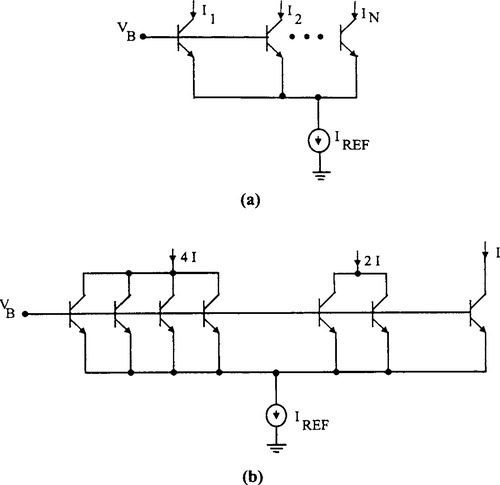
While conceptually simple, the implementation of Figure 3-49(a) has two drawbacks: the stack of current division transistors on top of IREF limits output voltage range, and IREF must be N times each of the output currents. This requires a high-current device for the IREF source transistor. There are techniques for alleviating these problems (Razavi, 1995). DACs that employ current division suffer from three sources of nonlinearity: current source mismatch, finite output impedance of current sources, and voltage dependence of the load resistor that converts the output current to voltage.
3.7.5 Charge Division
A reference charge, QREF can be divided into N equal packets using N identical capacitors configured as in Figure 3-50. In this circuit, before S1 turns on, C1 has a charge equal to QREF while C2,…,CN have no charge. When. S1 turns on, QREF is distributed equally among C1,…, CN yielding a charge of QREF/N on each. Further subdivision can be accomplished by disconnecting one of the capacitors from the array and redistributing its charge among some other capacitors.
While the circuit of Figure 3-50 can operate as a D/A converter if a separate array is employed for each bit of the digital input, the resulting complexity prohibits its use for resolutions above 6 bits. A modified version of this circuit is shown in Figure 3-51(a). Here, identical capacitors C1 = = CN = C share the same top plate, and their bottom plates can be switched from ground to a reference voltage, VREF, according to the input thermometer code. In other words, each capacitor can inject a charge equal to CVREF onto the output node, producing an output voltage proportional to the height of the thermometer code. The circuit operates as follows. First, Sp is on and the bottom plates of C1,…,CN are grounded, discharging the array to 0 (Figure 3-51(b)). Next, Sp turns off, and a thermometer code with height j is applied at D1,…, DN, connecting the bottom plate of C1,…, Cj to VREF and generating an output equal to jVREF/N (Figure 3-51 (c)). This circuit, in a strict sense, is a voltage divider rather than a charge divider. In fact, the expression relating its output voltage to VREF and the value of the capacitors is quite similar to that of resistor ladders. Nonetheless, in considering nonlinearity and loading effects, it is helpful to remember that the circuit’s operation is based on charge injection and redistribution.
The nonlinearity of capacitor DACs arises from three sources: capacitor mismatch, capacitor nonlinearity, and the nonlinearity of the junction capacitance of any switches connected to the output code. For details and implementation of capacitor DACs, see Razavi (1995).
3.7.6 DAC Architectures
With the basic principles of D/A conversion explained, we can study this function from architectural perspective. This section describes D/A converter architecture based on resistor ladders and current steering arrays, with an emphasis on stand-alone applications. While capacitor DACs frequently are used in ADCs, they have not been popular as stand-alone circuits.
3.7.6.1 Resistor Ladder DAC Architectures
The simplicity of resistor ladder DACs using MOS switches makes these architectures attractive for many applications. Simple ladder networks with simple voltage division as per Section 3.7.3 have several drawbacks: they require a large number of resistors and switches (2m, where m is the resolution) and exhibit a long delay at the output. Consequently, alternative ladder topologies have been devised to improve the speed and resolution.
3.7.6.1.1 Ladder Architecture with Switched Subdividers
In high-resolution applications, the number of devices in a DAC can be prohibitively large. It therefore is plausible to decompose the converter into a coarse section and a fine section so that the number of devices become proportional to approximately 2m/2 rather than 2m, where m is the overall resolution. Such an architecture is shown in Figure 3-52(a). In this circuit, a primary ladder divides the main reference voltage, generating 2J equal voltage segments. One of these segments is selected by the j most significant bits of (k + j) = m. If k = j, the number of devices in this architecture is proportional to 2m/2. It also is possible to utilize more than two ladders to further reduce the number of devices at high resolutions.
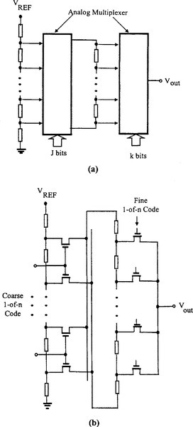
Figure 3-52(b) depicts a simple implementation of this architecture using MOS switches that are driven by one-of-n codes in both stages (Sheer, 1988). Depending on the environment, these codes are generated from binary or thermometer code inputs. The details and drawbacks of this implementation are discussed by Razavi (1995).
3.7.6.1.2 Intermeshed Ladder Architecture
Some of the drawbacks of ladder DACs can be alleviated through the use of intermeshed ladder architectures (Razavi, 1995). In these architectures, a primary ladder divides the main reference voltage into equal segments, each of which is subdivided by a separate, fixed secondary ladder. Figure 3-53 illustrates such an arrangement (Analog Devices, 1996), where all the switches are controlled by a one-of-n code.

The intermeshed ladder has several advantages over single-ladder or switched-ladder architectures. This configuration can have smaller equivalent resistance at each tap than a single-ladder DAC having the same resolution, allowing faster recovery. Also, since the secondary ladders do not switch, their loading on the primary ladder is constant and uniform. Furthermore, the DNL resulting from finite on-resistance of switches does not exist here.
3.7.6.2 Current Steering Architecture
Most high-speed D/A converters are based on a current steering architecture. Since these architectures can drive resistive loads directly, they require no high-speed amplifiers at the output and potentially are faster than other types of DACs. While the high-speed switching of bipolar transistors makes them the natural choice for current-steering DACs, many designs have been recently reported in CMOS technology as well.
3.7.6.2.1 R-2R Network-Based Architectures
To realize binary weighting in a current steering DAC, an R-2R ladder can be incorporated to relax device scaling requirements. Figure 3-54(a) illustrates an architecture that employs an R-2R ladder in the emitter network. A network with an R-2R ladder in collector networks is shown in Figure 3-54(b). For details, see Razavi (1995) and Hoeschele (1994).
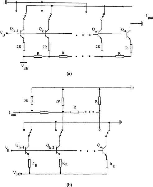
3.7.6.3 Other Architectures
Other architectures for DACs include segmented current steering versions, multiplying DACs, and Σ-Δ types. This chapter does not permit discussing these, so see Analog Devices (1995), Razavi (1995), and Hoeschele (1994).
3.8 Data Acquisition System Interfaces
3.8.1 Signal Source and Acquisition Time
Continued demand for lower-power, lower-cost systems increases the likelihood that a mixed-signal design will operate from a single 3.3 or 5 V power supply. Doing away with traditional ± 15 V analog power supplies can help you to meet your power and cost goals, but it also will eliminate some of your options.
Most low-voltage ADC and data acquisition system chips are designed for easy analog and digital interfaces. The ICs’ digital interfaces generally are compatible with popular microcontrollers, and the devices almost always can accept analog input signals that range from ground to the positive supply voltage; the span is set by an internal or external bandgap voltage reference. Virtually all ADCs that operate from 5 V or less are CMOS devices that use arrays of switches and capacitors to perform their conversions. Although the architectural details vary from design to design, the input stage of this type of converter usually includes a switch and a capacitor that present a transient load to the input signal source. The simplified schematic of Figure 3-55 shows how these input stages affect the circuits that drive them.

RON is not a separate component; it is the on-resistance of the internal analog switch. Sampling capacitor Cs connects to an internal bias voltage, whose value depends on the ADC’s architecture. In a sampling ADC, the switch closes once per conversion, during the acquisition (sampling) time. The on-resistance of the sampling switches ranges from about 5 to 10 k Ω in many low-resolution successive-approximation ADCs to 70 Ω in some multistep or half-flash converters. The capacitors can be as small as 10 pF in lower-resolution successive-approximation converters and 100 pF or more in higher-resolution devices.
When the sampling switch closes, the capacitor begins to charge through the switch and source resistance. After a time interval that usually is controlled by counters or timers within the ADC, the switch opens and the capacitor stops charging. The acquisition time described in Figure 3-10(c) is actually the time during which the switch is closed and the capacitor charges. As long as the source impedance is low enough, the capacitor has time to charge fully during the sampling period and no conversion errors occur. Most input stages are conservatively designed and can work properly at their rated speeds with a reasonable source resistance (1 kΩ is common). Larger source impedance slows the charging of the sampling capacitor and can cause significant errors unless you take steps to avoid them. Figure 3-56 illustrates this. Figure 3-56(a) indicates the case of insufficient acquisition time. Figure 3-56(b) shows a case in which the problem could be solved by slowing the clock. For further details, see Lancanette (1994) and Swager (1994).

3.8.2 The Amplifier-ADC Interface
Operational amplifiers nearly always are present in data acquisition systems, performing basic signal conditioning ahead of the ADC. Their interactions with ADCs affect system performance. Although many amplifiers are good at driving a variety of static loads, the switched nature of the ADC input stage can introduce problems with some amplifiers, especially the low-power, low-speed devices most likely to be used in 3 and 5 V systems. Using the simple model in Figure 3-57(a), the load presented to the amplifier by the ADC input keeps switching abruptly between an open circuit and a series RC response to the sudden load-current and impedance change depends on several parameters. Among them are the device’s gain-bandwidth product, slew rate, and output impedance.
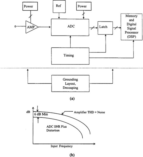
Selecting the appropriate drive amplifier for an ADC involves many considerations. Because the ADC drive amplifier is in the signal path, its error sources (both DC and AC) must be considered in calculating the total error budget. Ideally, the AC and DC performance of the amplifier should be such that there is no degradation of the ADC performance. Achieving this rarely is possible, however; therefore, the effects of each amplifier error source on system performance should be evaluated individually.
Evaluating and selecting op amps based on the DC requirements of the system is a relatively straightforward matter. For many applications, however, it is more desirable first to select an amplifier on the basis of AC performance (bandwidth, THD, noise, etc.). The AC characteristics of ADCs are specified in terms of SNR, ENOBs, and distortion. The drive amplifier should have performance better than that of the ADC so that maximum dynamic performance is obtained (see Figure 3-57(b)). If the amplifier AC performance is adequate, the DC specifications should be examined in terms of system performance. Table 3-6 summarizes the ADC drive amplifier considerations. Further details can be found in Analog Devices (1995).
Table 3-6
ADC Drive Amplifier Considerations
| Performance Requirements | Parameter |
| AC performance | Bandwidth, settling time, harmonic distortion, total harmonic distortion, noise, THD + noise |
| DC performance | Gain, offset, drift, gain nonlinearity |
| General | As a general principal, select first for AC performance, then evaluate DC performance Always consult the data sheet for recommendations |
Other considerations in interfacing are the input clamping and protection, drive amplifier noise configurations, ADC reference voltage considerations settling time considerations, and the like. These are beyond the scope of this chapter, and the reader is referred to Analog Devices (1992, Chapter 7; 1995; 1996), Lacanette (1994), and Swager (1994).
Interfaces between data converters and digital signal processors are discussed in Chapter 5.