
Programmable Logic Devices
10.1 Introduction
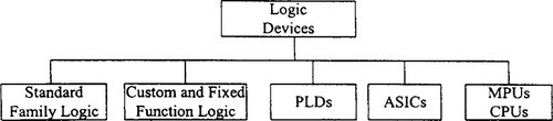
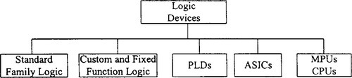
The ever-rising demand for huge amounts of data to move faster and faster through processors and networks has resulted in an endless sea of logic devices. To accomplish these tasks, semiconductor technology is moving toward speedier, more powerful processors and denser, more complex “glue chips” (devices that surround processors performing control logic functions) to manipulate information. The breadth of product offerings from the ASIC and programmable logic device vendors allows designers to select the device that is most cost effective for a target application. However, confusing terminology used by manufacturers (Maxfield, 1996) and various other reasons make choosing among these devices a trying task. Understanding the basic architectures around which these glue chips evolved, their progress, and their design methodologies will ease the task of selecting the right device for an application. Until 1970, most designers were using standard digital components in designing electronic products and systems. However, these fixed-function devices posed certain limits in achieving lower printed circuit board (PCB) real estate as well as product reliability due to the use of many interconnections. The need to design more compact digital circuits than is possible with standard digital components, without increasing design time and cost hampered design flexibility and led to the development of programmable logic. Figure 10-1 shows logic devices classified into five general types.
The programmable logic device (PLD) market has expanded in so many directions that the term has become a generic term for several subclasses of products, including programmable logic arrays, programmable array logic, programmable multilevel devices, and field programmable gate arrays. Programmable memories such as PROM, EPROM, and EEPROM are the earliest and simplest forms of PLD.
This chapter is an introduction to the designer who needs to use simple PLD applications and to identify the possibilities for using more complex forms of programmable devices such as field programmable gate arrays.
10.2 Basic Concepts
A PLD is an integrated circuit that is user configurable and capable of implementing digital logic functions. A typical PLD is composed of a programmable array of logic gates and interconnections with array inputs and outputs connected to the device pins through fixed logic elements such as inverters and flip-flops, based on the fact that all digital circuitry can be built using the basic elements such as NAND and NOR gates.
Any combinatorial logic function can be expressed as a sum of products: The variables are ANDed together to form products and the products are then ORed to form a sum. All PLDs are made up of combinations of AND gates, OR gates, inverters, and flip-flops. Programmable elements usually fuse connect the gates and flip-flops implement the desired logic functions. Each programmable logic device family requires a unique algorithm for fuse programming and verification on commercial programming equipment. The algorithm is a combination of voltage and timing required for addressing and programming fuses in the user array. The PLD’s programming circuitry is enabled by pulsing one or more pins to a specific voltage level, generally different from normal logic levels. Once the programming circuitry is enabled, inputs become addressing nodes for the input and product lines within the PLD. The actual fuse link is at the intersection of the input product lines. Once addressed, the fuse can be programmed by pulsing the output associated with the location of the fuse link. A fuse can be verified to be programmed by enabling the programming circuitry, supplying the fuse address to the device’s inputs, and reading the level of the device’s output. In erasable PLDs, the fuses can be reset, effectively erasing the old design, so the PLD can be reprogrammed with a new design. For an average PLD user, the actual method by which the PLD “stores” data is not all that important. Most of the good PLD development tools available today handle code implementation automatically, leaving the developer free to concentrate on code development.
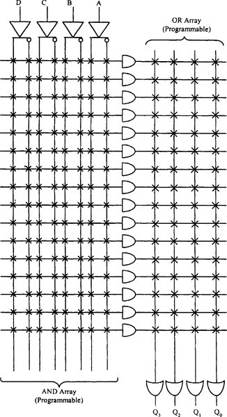
To keep the PLD easy to understand and use, a special convention has been adopted. Figure 10-2 is the representation of a three-input AND gate. Note that only one line is shown as the input to the AND gate. This line commonly is called the product line. The inputs are shown as vertical lines, and at the intersection of these lines are the programmable fuses. An x represents an intact fuse, which makes that input part of the product term. No x represents a blown fuse, which means that input will not be part of the product term. A dot at the intersection of any line represents a hardwired connection.
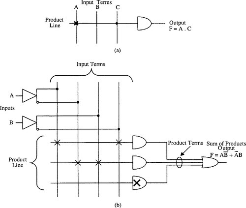
In Figure 10-2(b), the symbols are extended to develop a simple two-input programmable AND array feeding an OR gate. Note that buffers have been added to the inputs, which provide both true and complement outputs to the product lines. The intersection of the input terms forms a 4 x 3 programmable AND array. From these symbols, we can see that the output of the OR gate is programmed to the following equation, ![]() Note that the bottom AND gate has an x marked inside the gate symbol. This means that all fuses are left intact, which results in that product line having no effect on the sum term. In other words, the output of the AND gate will be a logic 0. When all the fuses are blown on a product line, the output of the AND gate always will be a logic 1. This has the effect of locking up the output of the OR gate to a logic level 1.
Note that the bottom AND gate has an x marked inside the gate symbol. This means that all fuses are left intact, which results in that product line having no effect on the sum term. In other words, the output of the AND gate will be a logic 0. When all the fuses are blown on a product line, the output of the AND gate always will be a logic 1. This has the effect of locking up the output of the OR gate to a logic level 1.
10.2.1 PROM as a Programmable Device
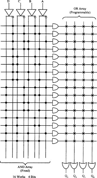
The PROM was the first widely used programmable logic family. Its basic architecture is an input decoder configured from AND gates, combined with a programmable OR matrix on the outputs. As shown in Figure 10-3, this allows every output to be programmed individually from every possible input combination. In this example, a PROM with four inputs has 24, or 16, possible input combinations. With the output word width being 4 bits, each of the 16 × 4 bit words can be programmed individually. Applications such as data storage tables, character generators, and code converters are just a few design examples ideally suited for the PROM. In general, any application that requires every input combination to be programmable is a good candidate for a PROM. However, PROMs have difficulty accommodating large numbers of input variables. Eventually, the size of the fuse matrix will become prohibitive, because for each input variable added, the size of the fuse matrix doubles.
10.2.2 PLD Architecture
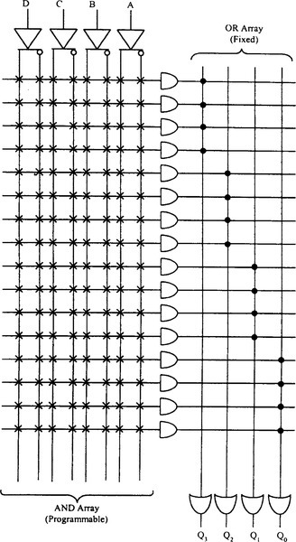
To overcome the limitation of a restricted number of inputs, the PLD utilizes a slightly different architecture, as shown in Figure 10-4. The same AND-OR implementation is used as with PROMs, but now the input AND array is programmable instead of the output OR array. This has the effect of restricting the output OR array to a fixed number of input AND terms. The trade-off is that, now, every output is not programmable from every input combination, but more inputs can be added without doubling the size of the fuse matrix. For example, if we were to expand the inputs on the PLD shown in Figure 10-4 and on the PROM in Figure 10-3 to ten, we would see that the fuse matrix required for the PLD would be 20 × 16 (320 fuses) vs. 4 × 1024 (4096 fuses for the PROM). It is important to realize that not every application requires every output to be programmable from every input combination. This makes the PLD a viable product family.
Simple PLDs such as programmable array logic (PAL™ of Advanced Micro Devices) and generic array logic (GAL™ of Lattice Semiconductor) derive their usefulness from an internal structure designed to allow the programming of either arbitrary products or sums or both. For example, PAL devices have a programmable AND-array and a fixed OR-array (Figure 10-4). PAL devices have two basic versions, with and without memory elements (flip-flops). Combinational PALs are devices that are based on a PAL structure but contain no memory elements. Combinational PALs are useful for a wide variety of random logic functions, including decoders, interface logic, and other applications that require a simple decoding of device inputs. The 16 L8, a typical combinational PAL, is diagrammed in Figure 10-5. The diagram for the 16 L8 shows that the device has ten dedicated inputs (pins 1 through 9 and 11) to the programmable AND array. Each input to the array is available in its true or a complemented form, allowing any combination of the inputs to be expressed on any row of the array. Each row of the 16 L8 array corresponds to one product term of the device.
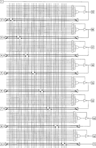
The 16 L8 has eight output gates, each of which is fed by a seven-input OR gate. Each output of this device is capable of implementing a logic function composed of seven or fewer product terms. The eighth product term is used to control the three-state output buffer.
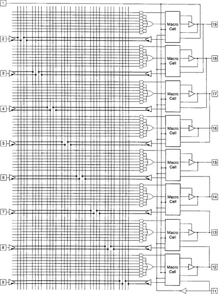
Some devices, such as GAL family from Lattice Semiconductor, integrate an output logic macro cell on some or all of their output pins (Figure 10-6). The macro cell is configured by the designer on a pin-by-pin basis to implement the desired functions. This allows design of synchronous logic blocks.
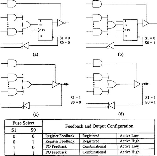
PLDs equipped with output macro cells offer total output flexibility. Figure 10-7 shows examples of these features as implemented in the TIBPAL22V10 device. Fuses SO and SI allow selection between registered or combinational outputs as well as output polarity. Figure 10-8 illustrates the user options.
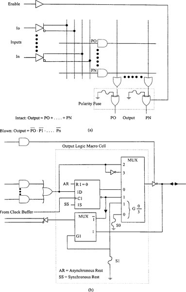
The user options are as follows:
1. Clock polarity select. The clock signal can be inverted via a clock polarity select fuse. This allows the transition of the register output to be on either the positive or negative edge of the clock pulse.
2. Internal-state registers. Several devices offer internal-state registers, often called buried registers. With the internal-state register, the output of the register is fed back into the AND array rather than to an output pin. This feature can be used for timing control sequences.
3. Variable product terms. Some PLD device architectures vary the number of product terms associated with each output pin to allow better utilization of the programmable array.
There may be variations of these in practical devices from different manufacturers (Dettmer, 1990; Hannington, 1990; Small, 1987, 1988).
10.2.3 FPLA Architecture
The field programmable logic array (FPLA) goes one step further in offering both a programmable AND array and a programmable OR array (Figure 10-9). This feature makes the FPLA the most versatile device of the three but impractical in most low-complexity applications. For applications in which complex timing control is required, Texas Instruments (TI) offers several programmable state machines based on the FPLA architecture. Some of these devices incorporate internal state registers or on-chip binary counters to aid in generating complex timing sequences.
10.2.4 Erasable PLDs
Another type of programmable logic device is the erasable programmable logic device (EPLD). Based on traditional PLD architecture, these devices typically offer a higher level of flexibility in the input and output configuration, register selection, and clocking options. CMOS EPLDs provide a higher level of density over standard PLDs and have lower power dissipation than bipolar PLDs. All programmable logic approaches discussed have their own unique advantages and limitations. The best choice depends on the complexity of the function being implemented and the current cost of the devices themselves. It is important to realize that a circuit solution may exist for more than one of these logic families.
10.3 Advantages of Programmable Logic
Low-density PLDs offer many advantages to the system designer presently using several standard catalog small scale integrated circuit (SSI) and medium scale integrated circuit (MSI) functions. The following list mentions just few of the benefits achievable when using programmable logic:
• Package count reduction. Several MSI/SSI functions can be replaced with one PLD to reduce system power requirements.
• PCB area reduction. Fewer devices consume less PCB space.
• Circuit flexibility. Programmability allows for minor circuit changes without changing the PC board.
• Improved reliability. With fewer interconnections, overall system reliability increases.
• Shorter design cycle. When compared with standard-cell or gate-array approaches, custom functions can be implemented much more quickly.
• Proprietary design protection (fuse protection). Circuit can be protected by blowing the security fuse.
• Minimization of design labor. Advantages of PLD computer-aided design tools could help save time in logic implementation.
10.4 Designing with PLDs
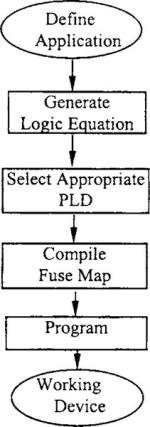
Figure 10-10 shows a basic PLD design flowchart. The best way to demonstrate the unique capabilities of the PLD is through a design example. With the design example given later, the user will gain the basic understanding on how to design a PLD application using design tools.
10.5 Design Tools for PLDs
An important secondary issue to choosing and using PLDs is selecting the right design tools (Liebson, 1990; Conner, 1990; Schulze, 1991). Design tools for PLDs comprise compilers, simulation products, and test software. Compilers convert the design into a fuse map; simulation products allow testing the design before programming a PLD to make sure that the design is right. Test software, which includes fault graders and automatic test pattern generators, helps keep things right during production.
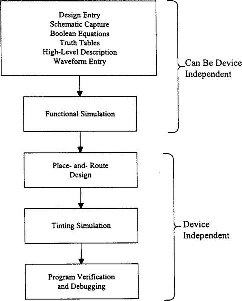
A number of software products are available to make logic designs easier and less cumbersome. When choosing a design tool, understanding the design process involving PLD designs and the key differences in design tools is necessary to help narrow down the choices. Figure 10-11 shows the typical design steps involved in designing with PLDs. The first step is to enter the design, and the common design entry methods are shown in Figure 10-11. Not all compilers support every design entry method. Schematic and Boolean entry methods remain popular among PLD designers, as they work well with 7400 TTL-style designing.
Many PLD compilers allow creating a design without regard to a particular device architecture. These compilers accept device specifications and allow post-poning device selection until much later. Device specificity introduces one of the first criteria you must consider when selecting a PLD compiler. Another key factor involved in selecting a compiler is good optimization performance. Good optimization centers around the compiler’s ability to generate device solutions that require minimal resources for a given logic function. Logic reduction algorithms eliminate redundant elements while preserving the required functionality. Different types of architecture often require different optimization techniques to maximize their use.
After optimization, a device must be selected with the physical resources necessary to implement the reduced equations. Most compilers can partition a design by trying single and multiple PLD solutions to create the “best fit.” Some engineers appreciate a compiler’s ability to partition. However, others know what PLDs they want to use and are not interested in the compiler’s ability to partition. Even if familiar with all the devices a designer may wish to use, partitioning software can explore many more possibilities in far less time than by hand. Furthermore, some compilers will allow creating subset libraries that contain just the PLDs in the designer’s lab stock or on a company’s approved list, eliminating obviously useless choices when generating alternative solutions.
Most PLD compilers include some sort of simulation capability. However, sometimes simulators may have to be purchased separately to fulfill particular requirements. The simulators with the least capabilities accept input and output vectors created by the designer and simulate the designer’s logic equations to ensure that the equations produce the results expected. More complex simulators use a model of a target PLD to create a simulation that reproduces the behavior specified. For this type of simulation, the designer specifies the input vectors, and the simulator generates output vectors or waveforms. The results can be checkedto see if a design works as expected. Thus, the designer finds out how the circuit will behave instead of guessing and verifying that guess.
After obtaining satisfactory results from the functional simulation, the next step is to run the place and route software. This is a critical step to get accurate timing simulation. There will be numerous possible routings, and it is difficult to comment on the ability of the routers to successfully route designs that meet tough timing requirements. Although users prefer placing and routing to be completely automatic, most do not want to run into a brick wall if the automatic software cannot handle the job. Some vendors offer an interactive design editor which allows manually tidying up things. Once the routing is complete, the next step will be to verify the timing, by loading the timing information generated by the place and route software into a simulator and running the timing simulation. The final step is to verify that the program has been correctly loaded into the device and debug. Most PLD problems can be found and corrected with no significant cost or schedule impact.
To achieve satisfactory programming yields for PLDs, it is critical that the device programmers adhere to the programming algorithm specifications as defined by the device manufacturer. Some helpful hints for good programmability follow:
1. Follow accepted standards for electrostatic discharge (ESD) protection. Equipment, personnel and work surfaces should be grounded. Air ionization is recommended when handling static sensitive devices outside protective containers.
2. Misaligned connectors and worn sockets can contribute to poor programming yield. Be aware of the manufacturer’s specification for number of insertions and be sure sockets are replaced frequently to ensure proper contact.
3. Be sure to use the latest update. Most program manufacturers offer updates and repair services to their users. The cost of service typically is not much more than the cost of a single update and the manufacturer may update four or more times per year.
4. Programming equipment should be calibrated. It is recommended to have no less than two calibrations per year.
5. Verify that the correct family pin-out codes or device entry codes are being used. It is important to understand that different algorithms may be needed for different speed versions of the same function.
6. Ensure that the programming equipment is evaluated and approved by the device manufacturer for highest possible programming yields and quality level.
In addition to the functional testing described earlier, static parametric testing such as input and I/O leakage currents, output high and low voltages under static loading, and power supply current will only improve the quality of the PLD going into the application. This will ensure that devices are functional and were not damaged due to ESD or electrical overstress (EOS) during the customization process.
The CUPL (Logical Devices Inc.), PL Designer (MINC Inc.), and ABEL (Data I/O) are universal computer-aided design (CAD) tools that support PLDs. With these software products, complex designs diagrams, and schematic capture methods available on most CAD systems.
ABEL consists of a special purpose, high-level language used to describe logic designs and a language processor that converts logic descriptions to programmer load files or JEDEC files. These files contain the information necessary to program and test PLDs.
The ultimate function of these software products is to generate a JEDEC file of the original design and program the PLD. However, most software vendors provide more than a JEDEC file as output from the software. Here, we describe the attributes of a few of the popular logic design products. We recommend contacting specific manufacturers to obtain the latest and most comprehensive information available.
The CUPL (universal compiler for programmable logic), like ABEL, is a universal CAD tool that supports PLDs. It has utility files that facilitate conver-sion of designs done in other design software environments to the CUPL design environment. CUPL also produces a standard programmer load file in JEDEC format, making it compatible with logic programmers that accept JEDEC files. Some features of CUPL design language follow:
• Flexible forms for design description. The forms include Boolean equations, truth tables, and state diagrams.
• Expression subsitutions and time-saving macros. This involves the assignment of names to equations and having the software do the substitution any time the assigned name is encountered during the compiling process.
• Shorthand features. These features include list notation, bit fields, distributive properties, and De Morgan’s theorem. List notation means the nested directive
[A4, A3, A2, Al, A0]
can be represented as
[A4 ..0]
Bit fields means that a group of bits may be assigned to a name as in
FIELD ADDR = [A4…0]
In the use of distributive property,
A & (B # C)
is replaced with
A & B # A & C
In De Morgan’s theorem,
(A & B)
is replaced with
! A # ! B
• The CUPL language processor. CUPL provides design templates that allow designers to just fill in the blanks when originating a design. Free form comments can be used throughout the design.
• Error checking. Error checking with detailed error messages directs designers to the source of problems during debugging.
• Logic equation reduction. The logic equation reduction capabilities on CUPL offers a choice of several minimization levels for a number of product terms. This can be from just terms to an optimum, before finalizing the fuse map of the PLD.
• Design simulation. This is accomplished using the CSIM feature, which allows designers to check the workability of the design before a part is programmed. Functional simulation can be done by the programmer when test vectors are provided.
10.6 A Design Example
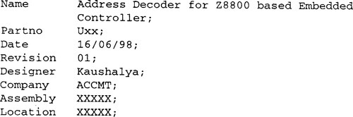
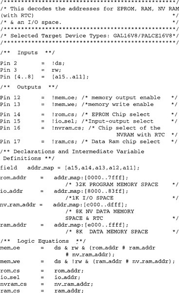
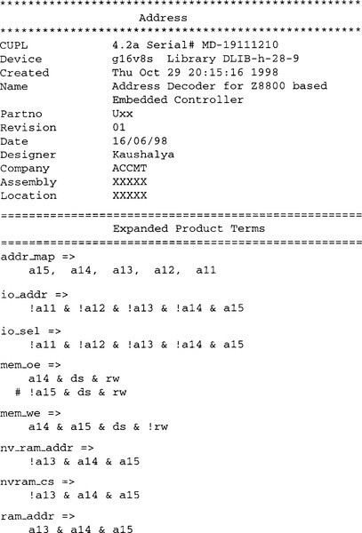
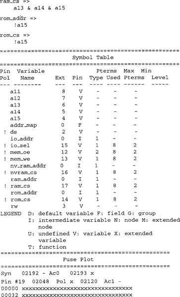
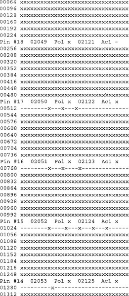
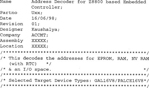
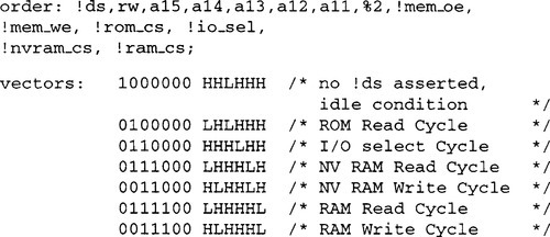
We take a simple example of an address decoder, as per Figure 10-12. This block illustrates the address decoding and generating the control signals in a memory-mapped Z8800-embedded application.

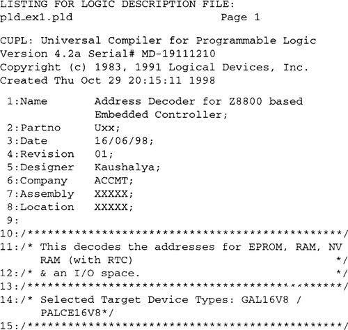
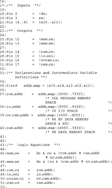
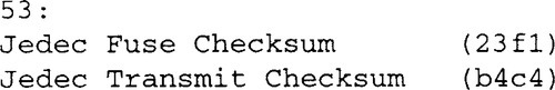
The PLD is expected to generate the chip select and control signals for the peripherals, as listed under output in the listing as per Listing 10.1. This is based on the package CUPL. Listing 10.2 is a comprehensive description of the logical expressions. CUPL creates expanded product terms, a variables list, a fuse plot, and the chip diagram (Figure 10-13) as per Listing 10.3.


10.7 High-Density PLDs
Even the largest PLAs and PALs can achieve integration levels equivalent to only a few hundred gates. The limitations on low-density PLDs are attributable to the rigidity of the AND-OR plane organization and its inability to perform any sequential or counter register functions at a rudimentary level.
As the progress of semiconductor technology made higher integration levels possible, high-density PLDs such as CPLDs and FPGAs emerged. The present marketplace of PLDs can be further classified into the following families (Figure 10-14):
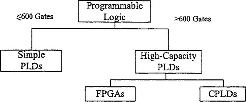
1. Programmable array logic (PAL).
2. Simple PLDs (SPLDs).
3. Complex PLDs (CPLDs).
4. Field programmable gate arrays (FPGAs).
CPLDs (sometimes called super PALs; Motorola Inc., Application note AN-1615) essentially are a large collection of PAL-like structures on one chip, desirable for designs that have tight speed requirements. FPGAs, on the other hand, consist of arrays of logic blocks connected by rows and columns of programmable interconnection lines and excel at designs that require large numbers of registers.
Choosing CPLDs or FPGAs or both for a design requires understanding the strengths of each (Swager, 1992; Miller, 1993). CPLDs usually are a better choice for designs that have very tight speed requirements, simply because of their deterministic timing. This is not to say that CPLDs will be the fastest implementation of a design but simply that the final speed will be fairly predictable at the beginning of the design cycle. Creative FPGA design can result in very fast logic, but it also can require time-consuming attention to the placement and routing details of internal logic blocks. Generally, CPLDs excel at implementing large amounts of combinatorial logic, and FPGAs excel at designs that require large numbers of registers. For example, implementing control functions such as state machines depends on taking advantage of the architectural features of the device being used. If encoding is used to develop a state machine, the resulting logic tends to work best in logic devices having lots of combinatorial gates and few registers, such as CPLDs. On the other hand, if a bit-per-state mapping method is used to develop a state machine, the design will require more registers but few logic gates, which can be best implemented using FPGAs. A comprehensive description of these devices and designing with CPLDs and FPGAs are beyond the scope of the chapter.
If a design is dense, requiring more than 20,000 gates and high-volume production is expected, the best choice for implementation would be full-custom ASICs or standard cell-based designs (Neigh and Bishop, 1988; Napier, 1992). In full-custom ASICs, including cell-based systems and optimized arrays, there is no preprocessing of the silicon and the designer can place any structure onto the design. In cell-based designs, circuit elements such as D-types and full addresses are predesigned. The designer places these in position and forms the connections between them. This generally is done manually and requires a detailed knowledge of silicon technology.
Recently, PLDs, particularly FPGAs, have been gaining momentum designs with fewer than 20,000 gates. High-density PLDs are starting to break the price barrier that kept them from volume applications. Keeping in mind that mask-programmed gate arrays are faster and more capacious than FPGAs, logic designers have several product development paths they could embark on (Small, 1992):
• Do an FPGA design, reserving the option to convert the FPGA to a mask-programmed gate array later.
• Do a multiple FPGA design, reserving the option to convert the FPGA to a single mask-programmed gate array later.
• Do an FPGA/multiple FPGA and mask-programmed gate-array design in parallel, using FPGAs for prototypes or initial production runs.
Several companies offer FPGA-to-ASIC conversion to achieve these goals. Historically, designers have viewed PLDs as prototypes and used gate arrays for more cost-effective high-volume applications. However, high-density PLDs are making inroads on territory that traditional ASICs and gate arrays once dominated.