
Chapter 10
Response of an Insulating Material to an Electric Charge: Measurement and Modeling 1
10.1. Introduction
In this chapter, we will take an interest in the observable response of an insulator subjected by its environment to different configurations of charge and electric field. The application of a DC stress was favored here, but the results presented could be extended to the case of a low frequency AC stress.
The response generally depends on a superposition of the internal mechanisms presented in the previous chapters. The material displays a specific order at the atomic scale (more or less deducible from its chemical formula), a structure at the nanometric scale due to the interactions between neighboring molecules (in the case of polymers), defects and impurities, a structure at the micrometric scale (spherulites for polyethylene, grains for polycrystals), together with surface phenomena, free surfaces, voids, and possibly interfaces when dealing with composite materials. Phenomena at each of these scales will have an influence on the general behavior of the insulator, at least in given conditions of field, pressure or temperature.
Research scientists know that theory in this domain is generally not able to predict accurately, for a given material, the results of even a simple an experiment. Therefore, our only ambition here is to show, with examples, what the phenomenological descriptions of the most frequent insulation behaviors are and on which physical hypotheses they rely.
10.2. Standard experiments
We shall consider the following two classical types of measurements:
– case (a): the environment sets the potential, and the insulator response determines the charge at its boundaries. This is the case of capacitors and of most circuits where an insulator is used to separate conductors. We measure in this case the current flowing through the insulator.
– case (b): the environment deposits a charge (or sets a current) on the surface, and the potential is determined by the properties of the insulator. This situation is the most widespread case when the insulator is not included in an electrical circuit. We measure in this case a surface voltage (a null field being imposed at the surface of the insulator).
Figure 10.1. Electrostatic measurements: (a) measurement of i(t) at fixed potential; (b) measurement of V(t) at fixed charge

Case (a) is generally called a closed circuit, and case (b) an open circuit, though this definition is vague, as shown by the example of the “voltage decay” experiment, where the charge (by corona, or electron beam) of the open circuit (represented in 10.1(b)) generally begins at a constant current (case b), then continues at a constant potential (case a) after the surface has reached an equilibrium potential and, at the end of charging, the potential decays without any charge supply (case b again).
Similarly, it is generally assumed that case (a) is allowing a permanent regime, while case (b) corresponds to a transient regime. It is often true, but it is possible to measure a steady potential during the application of a current (an example being the mirror method), and current flowing from a short-circuited insulator has indeed to be transient.
10.3. Basic electrostatic equations
10.3.1. General equations
In electrostatics, the Maxwell equations relate the electrical displacement D (D = ε0E + P, where E is the electric field and P the polarization in the insulator), the charge density ρ and the current density j in each point of the insulator, by:
We can deduce from this that ![]() : the flux of
: the flux of ![]() is conservative, and therefore equal to the current measured in the external circuit. The quantity
is conservative, and therefore equal to the current measured in the external circuit. The quantity ![]() is called the displacement current density. It expresses the local polarization variations in the insulator.
is called the displacement current density. It expresses the local polarization variations in the insulator.
The current density includes several components, in the general case, such as diffusion for instance. We will only consider here conduction current, which is equal to the sum, for the different charge carriers, of the products of the electric field by their mobility μi and their density ρi:
If the material presents a given intrinsic conductivity σ, we shall separate this term to write ![]() . The second part of the expression is then relative to a non-homogenous charge – often injected from the outside (a space charge). We therefore get:
. The second part of the expression is then relative to a non-homogenous charge – often injected from the outside (a space charge). We therefore get:
In the following sections, we shall examine the influence of these three physical parameters – dipolar polarization, intrinsic conduction, and space charge – on the observables (ground current (a), or surface potential (b)).
10.3.2. Current measurement at a fixed potential: case (a)
In this case, the average field is imposed by the voltage difference between the boundaries of the insulator and, from the null field condition inside the electrodes, the surface charge on them may be deduced. The application of a voltage difference on a neutral insulator will impose at each of its points a field initially proportional to the applied potential, and the polarization phenomena of the dielectric will give rise to a displacement current, first as an “instantaneous” peak of charge (whose amplitude only depends on the external circuit) equal to the flux of ![]() and corresponding to the vacuum polarization, and then a slow charging current, equal to the flux of
and corresponding to the vacuum polarization, and then a slow charging current, equal to the flux of ![]() , with response times corresponding to the characteristic polarization time constants of the different material components. The practical result of this gradual polarization, called absorption current, is a current which decreases in time.
, with response times corresponding to the characteristic polarization time constants of the different material components. The practical result of this gradual polarization, called absorption current, is a current which decreases in time.
The absorption current of dipolar origin will be superposed onto currents related to conduction, but, at low DC polarization fields, it could remain predominant for weeks within the material (Figure 10.3.), while for 50 Hz AC, it will represent the major part of the measured current.
Following insulator polarization, it is also possible to proceed to short-circuit discharge current measurements. The average field in an insulator being brought to zero, a depolarization current flows in the circuit, corresponding to the relaxation of what has been polarized during the charging. Equal charge and discharge currents (in absolute value) indicates a predominance of dipolar phenomena. Above a certain value of field and temperature, we observe a higher value of the charge current, which is a sign of the outbreak of a conduction favored by the field during charging.
10.3.3. Voltage measurement at a fixed charge: case (b)
The boundary conditions, in this case, are a zero potential at the lower side of the insulator, and a null field outside the insulator (this can be guaranteed by the use of an electrostatic voltmeter using a voltage feedback loop, but otherwise it remains true as long as the field in the air remains negligible compared with the field inside the insulator).
Integration of equation [10.1] (Gauss’s theorem) then implies that the electrical displacement in every point of an insulator will be equal to the surface charge density existing between that point and the outside of the insulator. The charge distribution, being fixed initially from the outside, will then be the input quantity of the system. For a one-dimensional problem (wide plane capacitor of thickness L), the continuity equation may be written for every point as follows:
In the absence of conduction phenomena, the insulator charging could be described by ![]() , i.e. the potential rise will be:
, i.e. the potential rise will be: ![]() . Part of the applied charge will thus be compensated by the polarization phenomena, and the potential rise will then be weaker in the presence of the insulator. When a charging current is interrupted, the circuit is then open, and slow polarization phenomena will lead to a voltage decay
. Part of the applied charge will thus be compensated by the polarization phenomena, and the potential rise will then be weaker in the presence of the insulator. When a charging current is interrupted, the circuit is then open, and slow polarization phenomena will lead to a voltage decay ![]() .
.
In the case where polarization is stabilized, it can be described by a dielectric constant ε, and the measured voltage changes will then be related to conduction effects. We thus get:
In the same way as for current measurements, a neutralization of the insulator can be performed. However in this case, it is done by a transient transfer of charges on the insulator surface. This can be compared to a temporary short-circuit. We then measure a voltage return, which will essentially be due to the depolarization phenomena, but could also be the consequence of the return of a dissymmetric space charge towards the electrodes.
10.4. Dipolar polarization
The dielectric relaxation of most insulators, notably polymers, has a very low frequency component, related at the same time to internal molecular reorganizations, and to complex interfacial polarization phenomena. In a linear regime, we can model this response using the dielectric functions φD(t) and φE(t) involved in convolution relations between the electrical displacement and field:
φD and φE are not independent, the product of their Laplace transform being 1.
For a homogenous dielectric of thickness L, only surface-charged, the electric field will be constant in the insulator, and related to the potential by E=V/L. The displacement will then be equal to the free charge density q on the surface.
In the case of the application at t=0 of a voltage step (V(t)=Γ0(t)V0), we may deduce from [10.7a] the insulator absorption current, proportional to φD (t) according to:
(S being the surface of the insulator, and C0 its geometric capacitance).
In the case of the deposit at t=0 of a charge amount q0 on the surface (q(t) = Γ0(t)q0), we may deduce from [10.7b] the decay rate of the surface potential:
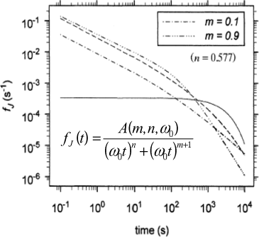
For reasons studied by Jonscher [JON 96] in particular, dielectric functions in condensed matter follow time power laws, according to Figure 10.2 (where the function fJ is equal to φD for t>0).
The logφE(t)=f(logt) curve, and therefore the voltage decay, in the log(dV/dt)=f(logt) plot, also tends to be composed of one or two straight line segments, but with slopes different to logφD(t)=f(logt) or to the absorption current.
The dipolar phenomena described by a dielectric function present a linear dependence on the value and the sign of the voltage or the applied charge. The effects produced during the depolarization experiment, with current or return voltage, are, then, easy to predict from the results of the polarization experiment.
10.4.1. Examples
Figure 10.3 shows an example of absorption current measurements on 15 μm thick polypropylene films. It is clear that, for an identical 67 kV/mm field, the charge and discharge currents are superimposed until a certain temperature threshold, between 300 and 340 K, corresponding to the outbreak of a genuine conductivity (probably ionic).

Figure 10.4 shows the result of voltage decay and return experiments at 25°C on epoxy films (190μm thick). The dipolar phenomenon is predominant, and the nonlinear effects, attributed to the charge injection, only appear in positive polarity for fields above 15 to 20 kV/mm; this result has been confirmed on the same samples by PEA measurements, detecting a charge injection above 18 kV/mm.
10.5. Intrinsic conduction
The existence of an intrinsic conduction σ induces a shielding of all net charge present in a material because equation [10.2] will in this case be ![]() , which leads to:
, which leads to:
A constant intrinsic conductivity must therefore give rise to an exponential decay of any charge density present in the material, with a time constant equal to the product of its resistivity and its permittivity.
Intrinsic conduction is, however, in practice nearly zero at room temperature and a moderated field for most materials used in electrical insulation, whose energy bands present a large gap and, above all, an extremely weak effective carrier mobility. The observables measured in this case will first of all be of dipolar origin, or related to an injected space charge.
The outbreak of a intrinsic conduction within the volume requires the generation of a certain amount of mobile carriers, with a renewal rate which compensates for the recombinations. Only irradiation will be energetic enough to allow generation of electron-hole pairs by hopping over the forbidden band. However, for insulators presenting mainly shallow traps, or for materials at high temperature or subjected to a high field, the thermal detrapping of part of the inner trapped charge can lead to a non-zero intrinsic conductivity. This process, described by the Poole–Frenkel Law, manifests itself by a conductivity proportional to the exponential of the square root of the electric field, divided by kT.
10.5.1. Example: charged insulator irradiated by a high-energy electron beam
During a voltage decay measurement, when a genuine conductivity exists in an insulator, the decay must be exponential, following the relationship:
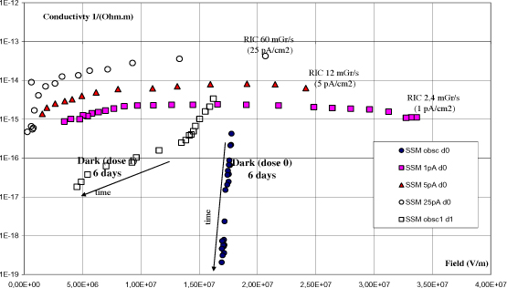
This parameter is plotted in Figure 10.5, as a function of the average field in the insulator during a voltage decay measurement on Teflon samples charged by a 25 keV electron beam, and submitted to increasing irradiation doses by a 400 keV beam, flowing through the insulator. The effect of the irradiation is to create a genuine conduction, lacking in the case of a non-irradiated insulator, which is a function of the dose rate. We also see that this effect remains perceptible several days after stopping the ionizing beam.
10.6. Space charge, injection and charge transport
Numerous models concerning the injection and transport of space charges have been developed. We can roughly classify them in four groups, depending on the way the properties of the material and interfaces are taken into account concerning injection and charge transport. The first three groups are models in which the dynamic is assumed to be set by the volume of the material, whereas for the fourth group, it is determined by the interfaces.
10.6.1. Electrostatic models
Charge trapping and detrapping are not taken into account here, and the charge transport is only determined by a mobility value μ: the charge motion only depends here on the local electric field ![]() .
.

Considering case (a), the average field in the insulator is fixed from the outside, but not the local field, which depends on the space charge inside the material. The field is therefore reduced, or even cancelled, in the insulator in the vicinity of the injecting electrode. The corollary of this lower field on one side of the material is an increase of the field – and therefore of the image charge – on the ground electrode: a current measurement on this electrode will hence detect the motion of the charge in the bulk of the material. The transient regime when a DC step voltage is applied is characterized by a rapid increase of the current during the injection phase, followed by its decay, due to the reduction of this injection caused by the decrease of the field at the injection electrode. In steady-state, we observe a characteristic space charge limited current (SCLC) regime, proportional to the square of the applied voltage.
Considering case (b), with a null field outside the insulator, the charge distribution can be considered as charge sheets successively injected into the material. Each of them is subjected to a constant field during its drift, proportional to the charge amount separating it from the surface (Gauss’s theorem), so that it will move at constant speed, proportional to this amount; the distribution will therefore gradually broaden in a homothetical way. This type of model predicts a constant initial voltage decay rate dV/dt, and we find (as in the previous case) a quadratic dependence of this parameter as a function of the deposited charge. Further, the image charge on the ground electrode remains constant until complete transit of the first charge sheet (total electrostatic influence of the charge distribution on the ground plane). A current measurement on the ground electrode will therefore not detect the motion of the charges, unlike in the previous case, where the electrostatic influence of each charge is shared between both electrodes, and switches during the drift from the upper to the ground electrode.
10.6.1.1. Example: transient current measurements on polyethylene films
Figure 10.7 clearly shows the transition between a decreasing transient current regime, polarization-dominated, and a charge injection regime, above a field of about 15 to 20 kV/mm. The authors hesitate, however, to attribute the current peak to a transit time, as predicted by the theory evoked above. Indeed, we shall see later that trapping phenomena play a large part in the shape of such a curve.
10.6.2. Models combining electrostatics and thermodynamics: the influence of trapping and dispersive transport
A correct treatment of charge transport in a disordered material requires taking trapping into account. Trapping is a consequence of material disorder, but this disorder involves many different aspects, leading to a wide range of energies for the traps. The energetically shallow levels are usually consequences of a weak disorder, often more or less periodical: the depth of this kind of trap is typically less than 0.1 eV.
On the other hand, traps related to chemical defects, like oxygen vacancies in the oxides, generally produce much lower energy levels, around 3eV below the conduction band. This is considered deep trapping. The density of these deep levels is particularly high in polymers.
Modeling can include shallow traps by introducing an effective carrier mobility, representing the hopping conduction processes between the traps. In a closed circuit, the carriers are being renewed by an interface and absorbed by another, so that an equilibrium may rapidly be reached, when the occupation rate of these traps reaches a steady-state value everywhere in the material. This model is the same as the electrostatic model, with a change of the mobility value only. However, in an open circuit, the studied regime is necessarily transient, and we must take into account the dispersive character of the charge transport. This type of modeling has also been undertaken, assuming for instance a constant energy distribution of trap levels, or an exponential distribution.
Trapping in deep levels can be modeled as irreversible trapping, or by including a detrapping process – possibly assisted by the field and temperature. In the first case, the only possible permanent regime in a closed circuit (unless we reach trap saturation) is the complete freeze of the current by the trapped space charge; if we include detrapping, the current flowing into the insulator will be equal to the detrapped charge by a unit of time. This case is detailed in the following section.
10.6.3. Purely thermodynamic models: current controlled by detrapping
Time will play a key role in the evolution of charge distribution. At the beginning of the experiment, the charge distribution divides into shallow and superficial trap levels, proportional to the capture probabilities of these levels: the shallow traps being more numerous, the charge will therefore still be quite mobile. Then, it gradually gets trapped in deeper levels where it will become more stable. The charge’s average mobility will therefore decrease with time. Over a long time, when the mean transit time of the charge carriers is weak compared with their mean characteristic detrapping time, we can completely eliminate the geometric factor from the models, the detrapping kinetics being then the only factor determining the equilibrium current or voltage.
This progressive charge trapping phenomenon may be described by a demarcation energy:
Nc being the conduction states density, Nt the trap density, and τ0 the carriers lifetime in the conduction states. This demarcation energy at a given instant t can be considered as the energy below which at this moment the trap emission can be neglected, and above which the trapping levels may be assumed to be in equilibrium with the transport states. This energy is thus the boundary between filled deep traps and empty shallower traps. Within this modeling frame, the evolution of the measured current or potential with time will be directly determined by the shape of the energetic distribution of the insulator traps.
10.6.3.1. Example 1: short-circuit current during the discharge of a polyethylene film
During conditioning under stress, we assumed that the various trap levels of the insulator were charged proportionally to their density. We may deduce from the previous reasoning that, during discharge, the traps’ emission current at t is related to their energetic density at the corresponding demarcation energy N(Ed):
For current measurement experiments in closed circuit, we can deduce that plotting tI(t)=f(logt) provides an image of N(E) as a function of the trapping energy. This plot of the current during the discharge of a short-circuited polyethylene film after a 2h 800 V charge is given Figure 10.8.
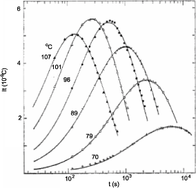
10.6.3.2. Example 2: voltage decay on a polystyrene film charged by an electron beam
Displaying a voltage decay measurement using a tdV/dt=f(logt) plot will also give a representation of the trap density. Figure 10.9 presents measurements for three different values of temperature, which are superimposed by shifting them in a way to represent them directly as a function of energy. We must point out, however, that this calculation mode under-estimates shallow trap density, since it neglects the influence of retrapping during the charge drift.
10.6.4. Interface-limited charge injection
The measured signal will be determined by the bulk phenomena evoked in the previous sections only if they are the main obstacle to charge displacement. In numerous cases, however, the measured signal will be determined by interface phenomena. The main reason for this is the energetic barrier existing at the metal– insulator contact, which also exists for surface charging by corona discharge ions.
In the first case (metal–insulator contact), the parameters for the barrier to cross essentially depend on the applied field. For moderated fields and temperatures above the ambient, the barrier will be crossed by means of thermoelectronic emission assisted by the field, and the Schottky law of current through this barrier will apply. For very strong fields, the barrier could be crossed without thermal assistance by field emission, and the law of current will then be the Fowler–Nordheim Law.
In the second case (with a non-metallic surface), the situation is more complex because the energies of deposited charges may be varied and they will evolve in time. We could then reuse models discussed in the case of gradual charge detrapping; the detrapping kinetics of the surface charge could determine the global behavior.
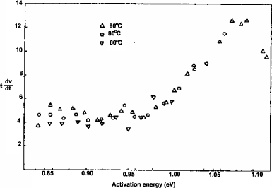
10.6.4.1. Example 1: stationary current in polypropylene films
Figure 10.10 shows current measurements on polypropylene films for different levels of field and temperature, using different data treatments. The graph on the left relies on a Schottky law hypothesis, i.e. a current limited by the thermoelectronic injection of carriers into the film. The determination of the permittivity value from the measured slopes makes this mechanism plausible, at least below 70°C and for moderated fields.

However, at 110°C as well as for fields exceeding 50kV/mm, the data treatment shown on the right, based on the hypothesis of a current limited by a hopping conduction in the volume of the insulator, is more suitable. Hence we come to the classical hypothesis of a transition, above a critical value of temperature and field, from a regime limited by electrodes to a regime limited by volume.
10.6.4.2. Example 2: voltage decay on corona-charged films
To account for voltage decay measurements on 6μm thick polypropylene films charged by corona at fields of about 200kV/mm, a decay limited by the detrapping of the surface charge had to be assumed. In this case, the charge density integrated within the film bulk was assumed to be weak compared with that present at the surface, and the transit time in the film assumed to be negligible compared with the characteristic time of surface charge detrapping [LLO 04].
10.7. Which model for which material?
The key issue to operate the variety of models presented here is to assess their validity for a practical situation with a given material and experimental conditions. The literature presents much experimental data, as current or voltage measurements, associated with the development of a model, followed by a discussion showing a good agreement between computed and experimental data. However, most often this evidence is not convincing because models based on different physical hypotheses, such as polarization of a disordered material, dispersive transport of an injected charge or gradual charge detrapping, may lead to the same time dependence of the measured value, composed of power laws, as shown in Figure 10.2. Nonetheless, the physical significance of the bend in the plot depends on the model: in the first case, it is a characteristic dipolar relaxation time; in the second, it is a spatial transit time; and in the third, it is a characteristic detrapping time. It is important to be aware of this difficulty and to carry out different tests to discriminate the phenomena as precisely as possible. Using sophisticated volume space charge measurement techniques may also provide important additional information, though it does not always allow injected charges from polarization heterogeneities to be distinguished.
In any case, the predominant mechanisms will depend on the stress level applied to the insulator. Thus, a measured current will generally appear, at low fields, with an ohmic appearance and be of dipolar origin. By increasing the field, the following scenario often occurs: a charge injection mechanism leads first, for intermediate fields, to a strong dependence on electrodes and field level described by a Schottky law, until a given field threshold is reached above which the current becomes volume-limited, implying a SCLC or hopping conduction law. At very high fields, electronic avalanches or hot electron phenomena will occur and lead to pre-disruptive pulsed phenomena.
Last but not least, the nature of carriers and microscopic conduction mechanisms is an important and difficult question which has not been considered here, where we favored a more macroscopic approach. The various mechanisms listed here do not rely on a particular hypothesis about the nature of charge carriers (whether electrons, holes, ions, etc.).
Insulator modeling cannot be reduced to considering one aspect or two (such as permittivity or conductivity), but reveals a wide diversity of phenomena. It cannot be done without testing the model with a variety of measurements.
10.8. Bibliography
[BER 03] BERLEZE S. M., ROBERT R., “Response functions and after effect in dielectrics”, IEEE Tr. Diel.&El. Ins., vol. 10, no. 4, p. 665–669, 2003.
[COE 93] COELHO R., ALADENIZE B., Les Diélectriques, Hermès, Paris, 1993.
[DAS 76] DAS GUPTA D. K., JOYNER K., “A study of absorption currents in polypropylene”, J.Phys. D: Appl. Phys., vol. 9, no. 14, p. 2041–2048, 1976.
[FOU 00] FOURNIÉ R., COELHO R., “Diélectriques. Bases théoriques”, Techniques de l’Ingénieur, D2300, p. 1–18, février 2000.
[FOU 90] FOURNIÉ R., Les isolants en électrotechnique: essais, mécanismes de dégradation, applications industrielles, Eyrolles, Paris, 1990.
[HAN 81] HANSCOMB J.R., GEORGE E.P., “Space charge and short-circuit discharge in high-density Polythene”, J. Phys. D: Appl. Phys., vol.14, no. 12, p. 2285–94, 1981.
[JON 96] JONSCHER A. K., Universal Relaxation Law, Chelsea Dielectrics Press, London, 1996.
[KIM 00] KIM D.W., YOSHINO K., “Morphological characteristics and electrical conduction in syndiotactic polypropylene”, J. Phys. D: Appl. Phys., vol. 33, no. 4, p. 464–471, 2000.
[LEV 06] LÉVY L., DIRASSEN B., REULET R., VAN EESBEEK M., MOLINIÉ P., “Dark and radiation induced conductivity on space used external coatings”, 10th Int. Symp. on Materials in a Space Environment, Collioure, France, 2006.
[LLO 02] LLOVERA P., Etude des mécanismes d’injection de charge dans les matériaux isolants au moyen de mesures électrostatiques de déclin et retour de potentiel. Nouveaux outils d’analyse, Doctoral Thesis, Paris XI University, 2002.
[LLO 04] LLOVERA P., MOLINIÉ P., “New methodology for surface potential decay measurements – application to study charge injection dynamics on polypropylene films”, IEEE Tr. Diel.& El. Ins., vol. 11, no. 6, p. 1049–1056, 2004.
[MOL 05] MOLINIÉ P., “Measuring and Modeling Transient Insulator Response to Charging: the Contribution of Surface Potential Studies”, IEEE Tr. Diel.& El.Ins., vol.12, no. 5, p. 939–950, 2005.
[RAJ 03] RAJU G.G. Dielectrics in Electric Fields, Marcel Dekker, New York, 2003
[SEG 00] SÉGUI I. “Diélectriques. Courants de conduction”, Techniques de l’Ingénieur, D2301, no. 5, p. 1–12, May 2000.
[WAT 95] WATSON P. K., “The transport and trapping of electrons in polymers”, IEEE Tr. Diel.& El. Ins., vol. 2, no. 5, p. 915–924, 1995.
1 Chapter written by Philippe MOLINIÉ.