
Chapter 11
Pulsed Electroacoustic Method: Evolution and Development Perspectives for Space Charge Measurement 1
11.1. Introduction
The presence of space charges (SC) in materials is a phenomenon which has been studied for many years [IED 84], [SES 97]. However, understanding of the generation, transport, and trapping modes of these charges has not yet been achieved. Amongst the numerous techniques developed to detect the presence of SC in materials [TAK 99], this chapter focuses on the pulsed electroacoustic (PEA) method.
During the past 20 years, much progress has been made concerning charge distribution detection in dielectrics through this technique. How this method is performed is in constant evolution, but the operating principle, which will be described in this chapter, remains unchanged [MAE 88].
In the first part of the chapter, we will endeavor to describe the general operating mode of the PEA system, and then, in part two, we shall list the diverse assemblies developed for specific applications. We shall outline the current systems’ limits and also the development perspectives that they open in diverse application areas.
11.2. Principle of the method
11.2.1. General context
The charges which accumulate during the application of an external excitation (electric field, irradiation, etc.) modify the material’s internal electric field and can cause an electrical breakdown in certain cases. The charges accumulation has been studied for a long time by techniques capable of giving information on the global quantity of charges, like the thermally stimulated depolarization current (TSDC) method [ENR 95] or surface potential measurement [MOL 00].
During the 1980s, diverse techniques were developed to study the charge distribution in the thickness of various samples. In most cases, a sample is placed between two electrodes; a charge displacement is imposed by an external stimulation, whose effect is to modify the influence charge on the electrodes. This modification is observed in the external circuit. The detected signal is transformed into a voltage variation through the sample in the case of a measurement made in open circuit, and in a current variation if we work in short-circuits. This type of measurement can only work if the external perturbation, which is applied to probe the material, undergoes a non-uniform modification in the volume direction and if its propagation is known over time.
The charges motion with respect to the electrodes can be controlled by a non-uniform expansion of the medium, as is the case when we heat one side of a sample [CHE 92] or by pressure wave generation [ALQ 81]. These methods, which are respectively known as thermal and acoustic methods, became popular very rapidly in Europe and North America. As its name indicates, the PEA method, whose principle we shall outline in detail later, belongs to the second category. Indeed, under the influence of a pulse voltage, the charges present in the studied material generate an acoustic wave while moving. This wave is transformed into an electrical signal by a piezoelectric captor for the analysis. This measurement technique was initially developed in Japan. Since the 1990s, this method, used in a routine manner in laboratories and on industrial sites, has also been well established in Europe [MON 00], [ALI 98], [BOD 04], [GRI 04].
11.2.2. PEA device
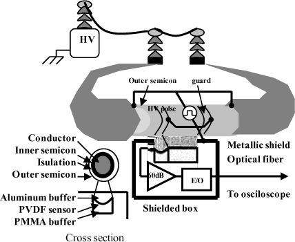
In a classic device (see Figure 11.1), the tested material is placed between two electrodes. From the upper electrode, it is possible to polarize the sample and apply voltage pulses which play the role of the probe to make the measurements.

One of the first conditions to obtain a charge profile is to use a pulse width much narrower than the transit time of the acoustic waves through the sample. Under the pulses influence, the volume or surface charges are moved in a sudden way by the Coulomb force. The moment exchange between the electrical charges connected to the atoms of the dielectric creates an acoustic wave, which then moves in the sample at the propagation speed of sound in the considered medium. A piezoelectric captor made of Polyvinylidene (PVDF) or Lithium Niobate (LiNbO3) converts this acoustic wave into an electrical signal, which is then amplified by preamplifiers before being visualized in an oscilloscope. The output signal width is closely related to that of the applied pulses.
Further, the resolution depends on the voltage pulse transmission quality at the sample. For this purpose, an electrical circuit composed of discrete resistances permits the transport line of the pulse to the electrode to be adapted to 50 Ω. A decoupling capacitance (typically Cd=250 pF) is placed between the adaptation circuit and the electrode to allow the simultaneous application of a polarization voltage. This capacitance being much bigger than that of the sample which is typically of the order of Cs=20 pF, the resulting capacitance is:
If the voltage applied to the sample is in the form:
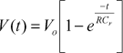
with V0 the applied voltage amplitude, R the resistance of the adaptation circuit with value 50 Ω, the time constant RCr is of the order of 1 ns, such that a weak distortion of V(t) is introduced. A study of electromagnetic compatibility with a network analyzer shows that the adaptation circuit was effective up to a frequency of 300 MHz. Beyond this value, complex resonance effects disturb the resistance bridge and the circuit impedance is no longer 50 Ω. The voltage pulses are typically supplied by a pulse generator with frequencies of the order of 400 Hz and amplitudes varying from 50 V to a few hundred volts. In general, pulses creating a field of about 1 kV/mm are selected to allow the measurement by perturbing the sample as little as possible.
A semi-conductor film is inserted between the excitation electrode and the sample in order to ensure a better acoustic impedance adaptation.
A high voltage is applied through a resistance of a few MΩ whose role is to limit the current in the case of sample breakdown.
The lower electrode is composed of an aluminum plate with thickness of about one centimeter. It plays the role of delay line between the analyzed acoustic signal and the electrostatic noise coming from the pulse generator. The piezoelectric film with surface of about 1 cm2 and a few micrometers thick (typically 4 µm) is placed under the electrode. An absorber is positioned under the piezoelectric captor to avoid the signal reflections.
By using a reference signal, recorded beforehand, it is possible to associate the raw signal amplitude with a charge density; the delay giving access to the charges distance with respect to the sample surface. Owing to this non-destructive method, the spatial charge distribution can be determined in the volume perpendicularly to the material’s surface.
11.2.3. Measurement description
We consider a sample of thickness ‘d’ in which there is a negative charge excess ‘q2’, situated at the distance ‘x’ from an electrode. Neutrality is obtained because of the presence of influence charges q1 and q3 at each electrode at x=0 and x=d respectively.
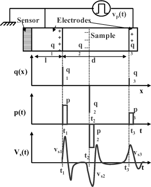
Under the action of short-duration pulses (between 5 and 9 ns), and with a high repetition frequency (400 Hz), charges are solicitated by the Coulomb force around their equilibrium position. Basic pressure waves stemming from each charged zone, with amplitude proportional to the local charge density in the sample, move at the speed of sound. We consider that the form of the pressure wave p(t) is identical to that of the pulsed electric field. The piezoelectric captor transforms the acoustic signal into voltage Vs(t), which is characteristic of the pressure considered. The piezoelectric system frequency response is not perfectly constant, so the signal Vs(t) complex form is distorted compared to the former pressure wave p(t). In order to obtain a precise charge distribution, a deconvolution technique was adopted. By processing the acoustic waves received at each instant, it is possible to determine the charge distribution when a voltage is applied but also during the depolarization phase.
11.2.4. Signal processing
To obtain a charge profile, the output signal must be deconvoluted. We consider here that the volume charge density of ρ(x) is distributed in the insulator (see Figure 11.2). For the study, we devised a sample in layers of thickness Δx in which we assumed that the charge density was homogenous. When a pulsed electric field e(t) is applied, a pressure fΔ(x, t) acts on each charge layer Δx and is given by the expression:
The pressure wave, obtained by dividing f by the surface S of the electrode, reaches the piezoelectric sensor without changing form. For this purpose, we hypothesize that the medium in which the acoustic wave propagates is homogenous and perfectly elastic.
The delay time between the moment when the wave is produced and the moment when it is detected depends on the speed of sound of each traversed material. We shall designate the speed of sound in the material as Vm, and the speed of sound in the electrode which is adjacent to the piezoelectric sensor as Ve. This thick electrode is, in most cases, aluminum.
The pressure thus seen by the detector is in the form:
The pressure which is exerted on the captor by the set of basic layers is obtained with a summation:
We note that the electric field is null outside the sample, and we can therefore limit the calculation for the interval x [0, d].
If we define τ = x/vm, and ρ(x) = ρ(τ.vm) = r(τ), we obtain:
As this latter equation is a convolution, it can be simplified by the application of the Fourier transform:
Similarly, the output signals vs(t) and entry signals p(t) of the piezoelectric sensor can be expressed by a convolution law in the Fourier space:
where Vs(v) and P(v) are, respectively, the Fourier transforms of vs(t) and p(t), and H(v) is the piezoelectric sensor transfer function characteristic, comprising the whole of the amplifiers and wave guides.
We recall that the goal is to measure the charge distribution profile in the materials. We just need to determine the transfer function H(v), which characterizes the sensor and the electronic components response to obtain R(v). This is possible using a reference signal.
The reference signal is recorded by polarizing an initially non-charged sample under a voltage U in the volume. The charge density (we designate here the capacitive charges) which is present at the electrodes is noted as:
We use index 1 to designate the data obtained during the calibration phase.
Since the pulse voltage amplitude up is much less than the polarization voltage U used to record the reference signal, we can consider that the detected capacitive charges are only caused by this latter. Thus, the pressure created by the charges at the electrode closest to the detector can be expressed in the following way:
and we obtain:
The properties of the piezoelectric sensor conversion properties always being the same, we have:
We can thus extract H(v) and, by combining the previous equations, we can obtain the expression F[ρ(x)]:
To obtain the value of ρ(x), we need to work out the following inverse Fourier transform:

To summarize, a charge profile determination requires two measurements. The first one allows vs(t) to be obtained, which will be converted with the Fourier transform into Vs(v). The second measurement (which corresponds to the reference signal) gives vs1(t), which will be converted into Vs1(v) by the same process.
11.2.5. Example of measurement
Any measurement starts with a reference signal recording. This measurement can be made on the material itself if it is not initially charged or on a material whose characteristics are known (propagation speed of sound, relative permittivity, etc.). This raw signal is visualized in an oscilloscope (see Figure 11.3). For signal processing, only the peak detected on the electrode situated near the piezoelectric sensor and the signal coming from the material volume are used.
Figure 11.3. Example of a reference signal recorded on a 1 mm polyimide sample, polarized below 5 kV and probed with 600 V pulses. Only the continuous line of the signal is used for deconvolution
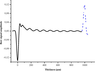
Figure 11.4. Example of PEA measurements obtained after deconvolution of signals recorded on a 1 mm polyimide sample polarized between -5 kV and 5 kV and probed with 600 V pulses. The reference had been recorded on the sample itself when it was polarized below 5 kV
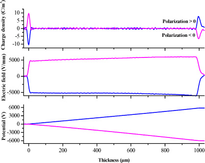
In the example of Figure 11.4, the charge profile corresponds to that of a polarized sample, which does not contain any charges in the volume after processing, because of the reference signal recorded beforehand.
Peak charges appear at the sample–electrode interfaces. The peak amplitude depends on the polarization amplitude and the polarity by a double integration. We can verify for each measurement that the electric field and potential profile correspond to the applied polarization.
11.3. Performance of the method
Formerly, this method was widely used to test electrical energy transport cable insulators [LIU 93]. Numerous results obtained on PolyEthylene (PE) samples or its by-products were published [LI 92], [FUK 06]. Since then, it has been commonly used for a wide sample group of materials ranging from solid materials [ALIS 98] to composite materials [TAN 06], to gels for biomedical applications.
The performance criteria lie in the spatial resolution and sensibility. Another important point concerns the speed at which the measurements can be made and repeated. As the resolution is determined by the entire measurement system’s signal-to-noise ratio, it is essential to reduce the noise coming from the outside (as, for example, that created by the pulse generator) but also that coming from inside (the thermal noise coming from preamplifiers, etc.).
11.3.1. Resolution in the thickness
The sample spatial resolution in the volume lies at first on the way the acoustic wave propagates. This resolution can be improved by reducing the acoustic signal width. As we have already seen, the acoustic wave is generated by application of an electric field; the duration during which the electric field is applied must be less than a few ns to generate an acoustic wave as narrow as possible. However, other factors must be taken into account, such as for example the oscilloscope bandwidth, the sensor geometry, the sample thickness. Indeed, the acoustic wave is detected by a piezoelectric sensor. Its thickness determines the resolution in volume of the signal. Over time, the spatial resolution, initially at 100 µm gets down to 5 µm [MAE 96], then 2 µm [MAE 98] by respectively using a 100 µm piezoelectric captor and an evaporated captor. Using these two factors, it is possible to improve the resolution which we shall call volumic. Classical systems generally offer a resolution of the order of 10 µm.
11.3.2. Lateral resolution
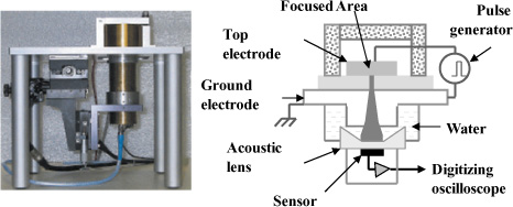
The classic PEA system allows a 2D charge distribution analysis in the sample’s volume. To obtain an observation in a third direction, we need to move the probe in diverse points on the material surface. The first developed 3D system [IMA 95] permitted the sample surface to be probed by the mechanical motion of the upper electrode. The resolution depended on the electrode area. During the first tests, knowing that the electrode had an area of 1 mm2, this resolution was estimated at 1 mm. Later, a PEA system equipped with a focus lens [MAE 01] permitted a 100 µm resolution to be achieved, the resolution depth being 5 µm for this system. This system’s operating principle and that of the latest developed will be described later.
11.3.3. Acquisition frequency
The PEA measurements must be repeated with a high repetition speed to be able to carry the signal and observe the transient phenomena. When a conventional mercury commutator is used, it is possible to observe a signal every 400 ms. The interval between 2 signals is 20 µs if we use a rapid commutator as a pulse generator, which permits the study of charge profiles evolution whose duration is of the same order.
11.3.4. Signal/noise ratio
The minimum amount of charge which can be detected by this method is about 0.1 C/m3. This value is extremely weak since it corresponds to a basic charge for 1011 atoms. However, such a charge can disturb an electric field of about 5 kV/mm on a 1 mm thickness.
11.4. Diverse measurement systems
Numerous system modifications were brought over time to obtain 3D measurements, for example, or measurements under constraints (high voltage, high temperature, vacuum-packed and during irradiation, etc.).
11.4.1. Measurements under high voltage
After charge distribution measurements validation for coaxial cable insulators [FUK 90], the PEA system was adapted to carry out tests under high voltage (up to 550 kV during breakdown tests) [HOZ 94]. In this device, 2 kV pulses with a 60 ns width are used. The interest in this system is that it allows testing directly on the cable at the manufacturing site (see Figure 11.5). In order to widen the measurements to all cable ranges, new modifications [FU 00], [FU 03] at the electrode level connected to the earth have been made over the past few years.
In the same way, a more classical system to measure thick planning samples submitted to high voltages (up to 150 kV) was developed for laboratory tests [HOZ 98].
11.4.2. High and low temperature measurements
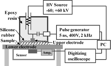
When the temperature increases, the carriers’ mobility and the trapping sites nature can vary strongly. This is why a system permitting measurements to be made in these conditions was developed. First, a cell comprising a thermo bath with silicone oil was used for a few studies [SUH 94]. In this case, the high voltage and the pulses were transmitted by a spherical electrode to limit the congestion around the sample and thus allow good temperature diffusion at the sample. The silicone oil bath can disturb certain materials’ properties and make their manipulation unsuitable for other tests, so measurements are now regularly carried out by placing the classic device in a thermally controlled enclosure. Tests up to 343 K and 85% humidity are frequently realized [KIT 96], [GAL 05].
The demand for measurements under much higher temperatures, for the study of ceramics for example, prompted the development of a PEA system with electronic parts cooling. Measurements up to 523 K were carried out [MIY 03]. However, as the temperature increases, a signal displacement in the time range is observed. This is caused by a decrease of the speed of sound in the aluminum electrode, which increases the signal transit time towards the sensor. The signals are stretched because the speed of sound is also reduced in the sample. We must take into account the modifications of the propagation speed of the signals for the analysis.
Conversely, dielectric studies made at cryogenic temperature for super conductor cable development allow measurements at 180 K and 290 K [MUR 01] without system modifications.
11.4.3. Measurements under lighting
Amongst functional polymers, photoconductor materials are widely used in photocopiers and electroluminescent devices. To complete the surface potential decline of these materials submitted to electric fields and to precise exposure to light, the manufacturers who make these materials rapidly demanded techniques to measure the internal charge distribution during their exposure. The first studies were undertaken by the Pressure Wave Propagation (PWP) method [TAN 92], but a PEA cell was rapidly developed to reply to the demand [SAT 96].
For these measurements, a semi-transparent aluminum electrode is sputtered on the irradiated surface, which permits voltage pulses to be applied during the lighting and thus allows the in situ evolution of the charge distribution in the volume.
11.4.4. 3D detection system
The first 3D charge profiles (see Figure 11.6) were obtained by moving the electrode by which the high voltage is applied [IMA 95]. Since this process is very slow, a new device was developed. An acoustic lens was thus introduced [MAE 01]. Only the acoustic waves generated at the focus point are detected by the piezoelectric sensor. To scan the sample surface, we need, in this case, to move the acoustic lens. Reasonably, 4 mm2 areas can be studied. The acquisition time depends on the number of points chosen for the analysis. The lateral resolution is about 0.5 mm and the volume resolution is 12 µm.
More recently, another system composed of multiple sensors (see Figure 11.7) was developed [TAN 03]. These sensors are positioned under the detection electrode and simultaneously receive a signal when probe voltage pulses are applied. The distance (typically 3 mm) between the PVDF sensors (whose dimensions are 2mm*3mm per side and 9 µm thick) determine the lateral resolution. To record the signals coming from the sensors independently, a coaxial switch is used.

11.4.5. PEA system with high repetition speed
To study transient phenomena such as the charge dynamics during a breakdown in a dielectric, it is fundamental to measure signals with a high repetition speed. Electric field pulses can be obtained by a generator with a rapid semi-conductor switch (available in shops).
The data recording can be realized by the new generations of oscilloscopes. The problem encountered is that of data storage and therefore their processing.
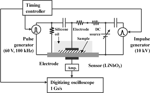
So far, two systems have been elaborated. The first is the PEA-3H (H for High, see Figure 11.8) [MAT 02]. It is a system which allows working under high voltage (in a domain which covers [−60 kV;+60kV]), with high repetition speed (2 kHz), and a large spatial resolution (10 µm). Faster systems (signal recorded every 20 µs) are restricted by the size of the oscilloscope’s memory. For long-lasting ageing tests, it is normal to record about 1,000 signals in 500 ms and to transfer them to a PC before the next set of data. This operation requires about 130 ms. The operation repetition for the whole duration of the test allows the breakdown phenomena to be studied in a fairly precise manner.
The second system is based on a high repetition speed and high temperature [FUK 04] (see Figure 11.9). This system can be used for breakdown studies. Silicone oil is used to guard the surface discharges and the partial discharges from the high voltage electrode. The temperature can be controlled. The generator delivers signals with a frequency of 10 kHz, which allow space charge profiles to be obtained every 10 µs and generally the observation time is limited to 1 ms before the next set of data.
11.4.6. Portable system
Since the demand for PEA measurements on industrial sites was increasing, a miniature system was developed. Indeed, the classic system configuration (measurement cell, oscilloscope and computer for data processing) did not predispose this technique to taking measurements at diverse points along a production chain, for example. Besides a size reduction, the form of the voltage pulses was improved to allow observation of direct charge profiles on the oscilloscope [MAE 03] (see Figure 11.10).
11.4.7. Measurements under irradiation
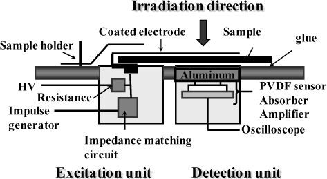
The charge distribution study in materials subjected to irradiation has become essential, notably in the space field, to understand electrostatic discharge phenomena which come up after a period of accumulation. The classic system was modified to allow measurements in a vacuum and also measurements during irradiation. The voltage pulse is applied either through a cone-shaped electrode [TAN 04] or an evaporated electrode [GRI 02] (see Figure 11.11).

11.4.8. Contactless system
In response to ever harder demands, in particular for measurements under irradiation, a contactless system was created. Under this system, the upper electrode is placed at a distance (approximately 1 mm) from the surface of the sample to be studied [IMA 04]. This surface is therefore floating and it is possible to detect charges left without disturbing anything. The disadvantage of such a system is the decrease in signal amplitude with the distance from the upper electrode, which turns out fundamental when the charge state of the studied system increases and the electrostatic discharge risk grows. The experimental protocol for the reference signal recording also has to be modified since the sample can no longer be polarized in the normal way.
11.5. Development perspectives and conclusions
Since its creation, the PEA method has never stopped being modified to allow measurements to be made in numerous configurations, and there is a good chance that efforts will continue, considering the increasing number of users of the method across the world. It is a tool which gives supplementary information to traditional measurements (current measurements for polarized materials, surface potential measurements for irradiated materials, etc.). New modeling axes are being created, owing to the data made accessible by PEA measurements. Indeed, the same material can be studied by the same technique with different measurement configurations and thus supply physical parameters concerning transport, such as mobility, trapping and recombination rates, etc.
This method offers the advantage of being relatively simple to implement in the sense that samples do not require special preparation. Signal processing is made by basic mathematical tools. The method offers the possibility of studying dynamic phenomena and can be used to study samples in which space charges were generated in a complex manner.
11.6. Bibliography
[ALI 98] ALISON J.M., “Pulsed electro-acoustic system for space charge and current density measurements at high fields over a temperature range 25°C–80°C”, Proceedings CSC’3, p. 711–714, 1998.
[ALIS 98] ALISON J.M., “A high field pulsed electroacoustic apparatus for space charge and external circuit current measurement within solid insulators”, Meas. Sci. Technol., vol. 9, p. 1737–1750, 1998.
[ALQ 81] ALQUIÉ C., DREYFUS, G., LEWINER J., “Stress wave probing of electric field distribution in dielectrics”, Phys. Rev. Lett., vol. 47, p. 1483–1487, 1981.
[BOD 04] BODEGA R., MORSHUIS P.H.F., SMIT J.J., “Space charge signal interpretation in a multi-layer dielectric tested by means of the PEA method”, Proceedings ICSD’04, p. 240–243, Toulouse, France, 5–9 July, 2004.
[CHE 92] CHERIFI A., ABOU DAKKA M., A. TOUREILLE, “The validation of the thermal step method”, IEEE Trans. Electric. Insulat., vol. 27, no. 6, p. 1152–1158, December 1992.
[ENR 95] ENRICI P., ROPA P., JOUMHA A., REBOUL J.P., “Space charge measurements by the thermal-step-method and TSCD in polymeric materials”, Proceedings IEEE ICSD’95 Virginia Beach, USA, p. 504–507, October 1995.
[FU 00] FU M., CHEN G., DAVIES A.E., TANAKA Y., TAKADA T., “A modified PEA space charge measuring system for power cables”, Proceedings 6th ICPADM’00, p. 104–107, juin 2000.
[FU 03] FU M., CHEN G., “Space charge measurement in polymers insulated power cables using flat ground electrode PEA system”, IEE Proc.-Sci Meas. Technol., vol. 150, no. 2, March 2003.
[FUK 90] FUKUNAGA K., MIYATA H., SUGIMORI M., TAKADA T., “Measurement of charge distribution in the insulation of cables using the pulse electro-acoustic method”, Trans. IEE Japan, vol. 110-A, no. 9, p. 647–648, 1990.
[FUK 04] FUKUMA. M., MAENO T., FUKUNAGA K., NAGAO M., “High repetition rate PEA system for in-situ space charge measurements during breakdown tests”, IEEE Trans. DEI, vol. 11, no. 1, p. 155–159, 2004.
[FUK 06] FUKUMA M., FUKUNAGA K., LAURENT. C, “Two-dimensional structure of charge packets in polyethylene under high DC fields”, Appl. Phys lett., vol. 88, no. 25, June 2006.
[GAL 05] GALLOT-LAVALLÉE O., TEYSSÈDRE G., LAURENT C. ROWE S., “Space charge behaviour in an epoxy resin: the influence of fillers, temperature and electrode nature”, J. Phys. D: Appl. Phys., vol. 38, no. 12, p. 2017–2025, 2005.
[GRI 02] GRISERI V., LÉVY L., PAYAN D., MAENO T., FUKUNAGA K., LAURENT C., “Space charge behaviour in electron irradiated materials”, Proceedings IEEE CEIDP’02, p. 922–925, 2002.
[GRI 04] GRISERI V., FUKUNAGA K., MAENO T., LAURENT C., LÉVY L., PAYAN D, “Pulsed electro-acoustic technique applied to in-situ measurement of charge distribution in electron-irradiated polymers”, IEEE Trans. Dielectr. EI., vol. 4, no. 5, p. 891–898, October 2004.
[HOZ 94] HOZUMI N., SUZUKI H., OKAMOTO T., WATANABE K., WATANABE A., “Direct observation of time-dependent space charge profiles in XLPE cable under high electric fields”, IEEE Trans. Diel. EI, vol. 1, no. 6, p. 1068–1076, 1994.
[HOZ 98] HOZUMI N., TAKEDA T. SUZUKI H., OKAMOTO T., “Space charge behaviour in XLPE cable insulation under 0.2-1.2mV/cm DC fields”, IEEE Trans. Diel EI, vol. 5, no. 1, p. 82–90, 1998.
[IED 84] IEDA M., “Electrical conduction and carrier traps in polymeric materials”, IEEE Trans. Electr. Insulat., vol. EI-19, p. 162–178, June 1984.
[IMA 95] IMAISUMI Y., SUZUKI K., TANAKA Y., TAKADA T., “Three-dimensional space charge distribution measurement in solid dielectrics using pulsed Electroacoustic Method”, Proceedings IEEE ISEIM’95, p. 315–318, 1995.
[IMA 04] IMAI S., TANAKA Y., FUKAO T. TAKADA T., MAENO T., “Development of new PEA system using open upper electrode”, Proceedings CEIDP’04, IEEE, p. 61–64, July 2004.
[KIT 96] KITEJIMA M., TANAKA Y., TAKADa, “Measurement of space charge distribution at high temperature using the pulsed electro acoustic method”, Proceedings 7th Int. Conf. DMMA’96, p. 8–11, Bath, UK, September 1996.
[LI 92] LI Y., TAKADA T., “Experimental observation of charge transport and injection in XLPE at polarity reversal”, J. Phys. D: Appl. Phys., vol. 25, p. 704–716, 1992.
[LIU 93] LIU R., TAKADA T., TAKASU N., “Pulsed electroacoustic method for measurement of charge distribution in power cables under both DC and AC electric fields”, J. Phys. D: Appl. Phys., vol. 26, p. 986–993, 1993.
[MAE 88] MAENO T., FUTAMI H., KUSHIBE T. COOKE C.M., “Measurement of space charge distribution on thick dielectrics using the pulsed electroacoustic method”, IEEE Trans. Electr. Insul., vol. 23, p. 433–439, 1988.
[MAE 96] MAENO T., FUKUNAGA K., TANAKA Y., TAKADA T., “High resolution PEA charge measurement system”, IEEE Trans. Diel. EI, vol.3, no. 6, p. 755–757, 1996.
[MAE 98] MAENO T., “Extremely high resolution PEA charge measurement system”, Report of Study Meeting IEE Japan, DEI-98-78, p. 81–86, 1998.
[MAE 01] MAENO T., “Three-dimensional PEA charge measurement system”, IEEE Trans. DEI, vol. 8, no. 5, p. 845–848, 2001.
[MAE 03] MAENO T., “Portable space charge measurement system using the pulsed electroacoustic method”, IEEE trans. Diel. EI, vol. 10, no. 2, 2003
[MAT 02] MATSUI K, TANAKA Y., FUKAO T., TAKADA T., MAENO T., “Short-duration space charge observation in LDPE at the electrical breakdown”, Proceedings IEEE CEIDP’02, p. 598–601, 2002.
[MIY 03] MIYAUCHI H., FUKUMA M., MURAMOTO Y., NAGAO M., MAENO T., “Space charge measurement system under high temperature on PEA method”, Proceedings IEE Jpn. CFM’03, no. 7–14, 2003.
[MOL 00] MOLINIÉ P., LLOVERA P., “Surface potential measurements: implementation and interpretation”, Proceedings. IEEth Int. Conf. DMMA’00, p. 253–258, 17–21 September 2000.
[MON 00], MONTANARI G.C., MAZZANTI G., BONI E., DE ROBERTIS G., “Investigating AC space charge accumulation in polymers by PEA measurements”, Proceedings IEEE ICSD’00, Victoria, Canada, p. 113–116, October 2000.
[MUR 01] MURAKAMI Y., FUKUMA M., HOZUMI N., NAGAO M., “Space charge measurement in EVA film at cryogenic-room temperature region”, Trans. IEE Jpn., vol. 121-A, no. 8, p. 758–763, 2001 (in Japanese).
[SAT 96] SATOH Y., TANAKA Y., TAKADA T., “Observation of charge behavior in organic photoconductor using the pulsed electroacoustic method and Pressure wave propagation Method”, Proceedings IEE 7th Int. Conf. DMMA’96, p. 112–115, 23–26 September 1996.
[SES 97] SESSLER G.M., “Charge distribution and transport in polymers”, IEEE Trans. Dielectr. Electric. Insulat. vol. 4, no. 5, p. 614–628, octobre 1997.
[SUH 94] SUH K.S., HWANG S.J., NOH J.S. TAKADA T., “Effects of constituents of XLPE on the formation of space charge”, IEEE Trans. Diel. EI, vol. 1, no. 6, p. 1077–1083, 1994.
[TAK 99] TAKADA T., “Acoustic and optical methods for measuring electric charge distributions in dielectrics”, Proceedings IEEE ICSD’99, vol. 1, Austin, USA, p. 1–14, octobre 1999.
[TAN 92] TANAKA A., MAEDA M., TAKADA T., “Observation of charge behavior in organic photoconductor using pressure-wave propagation method”, IEEE Trans. on Electric. Insulat., vol. 27, no. 3, p. 440–444, June 1992.
[TAN 03] TANABE Y., FUKUMA M., MINODA A., NAGAO M, “Multi-sensor space charge measurement system on PEA method”, Proceedings IEE Jpn. CFM’03, no. 7–14, 2003.
[TAN 04] TANAKA Y., FUKUYOSHI F., OSAWA N., MIYAKE H., TAKADA T., WATANABE R., TOMITA N., “Acoustic measurement for bulk charge distribution in dielectric irradiated by electron beam”, Proceedings ICSD’04, p.940–943, 2004.
[TAN 06] TANAKA H., FUKUNAGA K., MAENO T., OHKI Y. “Three-dimensionnal space charge distribution in glass/epoxy composites”, Proceedings 8th IEEE ICPADM’06, Bali, Indonesia, June 2006.
1 Chapter written by Virginie GRISERI.