
7
TAT Model Applications: Wear, Creep, and Transistor Aging
7.1 Solving Physics of Failure Problems with the TAT Model
In this chapter we provide examples of the thermally activated time-dependent (TAT) models that include degradation models for wear, creep, transistor aging, as well as dielectric leakage. We include both cases in the instant of field-effect transistor (FET) and bipolar transistors.
7.2 Example 7.1: Activation Wear
There are a number of different types of wear, often characterized by their wear rate [1, 2]. Activation wear is a term we use here to describe wear due to a thermally activated process. This approach offers an alternative to the Archard’s empirical constant-type-wear model discussed in Chapter 4 (see Equation (4.20)). Heat is often an enemy in degradation processes and leads to an acceleration effect in frictional wear. When logarithmic-in-time aging occurs, as is illustrated in Figure 7.1 (often observed in metals), the TAT model can apply. This is characterized by an initially high wear rate followed by a steady-state low wear rate. Archard’s type shows the case of steady wear in time, where the wear rate amount is constant over the sliding distance (Figure 7.1). Log(time) shows the case of an initially constant wear rate, where surface roughness increases to a certain value and does not increase much after that as the wear rate then decreases over sliding distance. The other type of wear is observed in lapping and polishing for surface finishing of ceramics.

Figure 7.1 Types of wear dependence on sliding distance (time)
Here we will focus on activation or log(time) wear and consider surface mass trapped in a potential well. We need to apply enough thermal energy (friction) for mass to escape from the chemical bonds. When a normal force is applied to the surface due to contact wear under a constant velocity, the normal force P results in material mass M removal (see Figure 4.3). We will start by taking a naïve kinetic friction approach
where μK,eff is an effective coefficient of sliding kinetic friction and the velocity ν is constant. Here we start with a simple kinetic frictional model to get the general form. For an activated process of mass removal, we write that the change in the mass per unit time is proportional to the normal force applied to the contact surface so that

where μK,eff(T) is a temperature-dependent effective kinetic coefficient of sliding friction which must be generalized. This can be written

where ![]() . We now have to depart from our naïve approach as kinetic friction, although insightful, is not helpful enough in accurately depicting the amplitude in wear. To be consistent and specify the model a bit further, we can use historical information such as the Archard’s wear model in Equation (4.20). We have a few options and can write the amplitude
. We now have to depart from our naïve approach as kinetic friction, although insightful, is not helpful enough in accurately depicting the amplitude in wear. To be consistent and specify the model a bit further, we can use historical information such as the Archard’s wear model in Equation (4.20). We have a few options and can write the amplitude
That is, we can either make use of the Archard’s amplitude or write the amplitude in experimental terms of an initial average mass removal ![]() and an average time constant for removal τ. This amplitude can be found experimentally as we will describe. We have added ρ, the density of the softer material, to Equation (4.20) for consistent units with mass removal and the other parameters defined in this equation. Expanding the free energy as a function of the mass removal we have
and an average time constant for removal τ. This amplitude can be found experimentally as we will describe. We have added ρ, the density of the softer material, to Equation (4.20) for consistent units with mass removal and the other parameters defined in this equation. Expanding the free energy as a function of the mass removal we have
We identify ![]() (see Equation (2.114) or (5.7)) as the activation chemical potential per unit mass, which now gives
(see Equation (2.114) or (5.7)) as the activation chemical potential per unit mass, which now gives
and ϕ is the activation energy for the wear process that can be found experimentally by testing at different temperatures as explained below. Rearranging terms, and solving for the mass as a function of time t and integrating, provides a logarithmic-in-time aging TAT model in terms of mass removal over time:
where A and B are
Note the logarithmic-in-time dependence in the activation wear case differs from Archard’s linear dependence (i.e., l = vt). Here we find that when Bt in Equation (7.7) is less than or of the order of 1, the removal amount is large at first then is less as time accumulates (non-linear in time removal). However, when Bt >> 1, the removal is in ln(t) dependence. Also since ln(1 + X) ~ X for X << 1, then Equation (7.7) can be approximated as ![]() for Bt << 1, which upon substitution of Equation (7.4) agrees with Equation (4.20), the Archard wear equation. Note that, one could make use of this early time approximation to help determine
for Bt << 1, which upon substitution of Equation (7.4) agrees with Equation (4.20), the Archard wear equation. Note that, one could make use of this early time approximation to help determine ![]() and the wear activation energy ϕ experimentally.
and the wear activation energy ϕ experimentally.
7.3 Example 7.2: Activation Creep Model
Activation creep is a term we use here to describe creep due to a thermally activated process where the activation free energy is a function of the strain itself. This approach offers an alternative approach to modeling the creep process. The general model indicates that for creep to occur under temperature activation that a number of dislocations will occur over time in the metal lattice (see Figure 3.1). This when, due to temperature stress, dislocations N have a probability of hopping over a potential barrier and weakening the crystal metal lattice. Its hopping rate of occurrence is (see also Equation (6.2))

where in the TAT model the activation energy is a function of N. In the case of creep, N would be proportional to strain. However, this relation must of course be modified when a load σ is applied and the material is also subjected to mechanical means. We will therefore add this using a popular form of the empirical creep rate equation, typically written

Note the difference from Equation (4.12) regarding the time dependence of this popular form for the creep rate. Also the key difference in this approach is that we associated the creep rate process with the activation free energy as a function of the strain itself. We will at this point use the TAT model by expanding it in terms of the strain dependence in a Maclaurin series:
We identify that the change in the free energy is due to damage that occurred from mechanical thermodynamic conjugate work (see Table 1.1 and Chapter 4):
This then yields

which is now in the form of the TAT model (see Equations (6.7) and (6.8)). We find on integration:
where

or
where

We note that we actually had to start with an empirical expression in Equation (7.10) for the creep rate. Once we expanded the activation free energy in terms of the strain, the creep rate indicated a non-linear time dependence ln(1 + Bt). The logarithmic-in-time dependence model has the common curvature found in primary and secondary creep stages (see Figures 9.5 and 9.6 for creep curves and compare to Figure 6.2). A power law dependence ε α t β where 0 < β < 1 is also popular as highlighted by Equation (4.12), and both the ln(1 + Bt) and power law form have been used by other authors [3]. (Also see Figure 6.3 on how a power law can be similar to log time aging rates.) Interestingly enough we see the stress amplitude is an inverse relation to strain, which of course by itself would be incorrect. However, the argument in the natural log function includes strain to the N + 1 power which, as long as N > 0, will actually show that the strain increase with stress. Finally, the activation energy should be the same ϕ(0) as reported in the literature. The third stage of creep can also be modeled using the TAT model. This concept is provided at the end of this chapter.
7.4 Transistor Aging
Here we illustrate how we can extend the TAT model to transistor aging [4]. We are primarily concerned with key transistor device parameters. In the bipolar case for the common-emitter configuration, the key transistor parameter is beta aging, showing it to be directly proportional to the fractional change in the base-emitter leakage current. In the FET case, the key transistor parameter considered is transconductance aging that results from a change in the drain-source resistance and gate leakage current. Then the TAT model is used to provide an aging expression that accounts for the time degradation of these parameters found in life test. These expressions provide insight into degradation that links aging to junction-temperature-dependent mechanisms. The mechanisms for leakage can be thought of as similar to a corrosion process having a corrosion current. All the components are similar (an anode, cathode, a conducting path, and an effective type of dielectric “electrolyte”). Some typical life test data on heterojunction bipolar transistors (HBTs) and metal semiconductor field-effect transistor (MESFETs) are illustrated.
7.4.1 Bipolar Transistor Beta Aging Mechanism
Bipolar transistor degradation over time is a serious issue in microelectronics.
Generally, there are two common bipolar aging mechanisms: an increase in emitter ohmic contact resistance and an increase in base leakage currents.
Both can be thought of as corrosion-occurring process. Since β is given by Ice/Ibe in the common emitter configuration, any base leakage degradation in Ibe will degrade β. In this section, we describe a model for β degradation [4] over time due to leakage. We start by considering a change in the base current gain for the common emitter configuration as
where β0 is the initial value (prior to aging) of Ice/Ibe. The time-dependent function Δβ(t) can be found through the time derivative:

Approximating d/dt by Δ/Δt, and noting that Δt is common to both sides of the equation and cancels, yields

In the above equation, ΔIce has been set to zero as no change in this parameter is usually observed experimentally. We added the absolute value sign since beta overall will degrade ![]() as the leakage current to the base increases. The first result is therefore that the change in β is directly proportional to the fractional change in the base-emitter leakage current:
as the leakage current to the base increases. The first result is therefore that the change in β is directly proportional to the fractional change in the base-emitter leakage current:

The last expression for the voltage follows from the next section.
7.4.2 Capacitor Leakage Model for Base Leakage Current
At this point, base charge storage is discussed in order to develop a useful capacitive model. When a transistor is first turned on, electrons penetrate into the base bulk gradually. They reach the collector only after a certain delay time τd. The collector current then starts to increase in relation to the current diffusion rate. Concurrent with the increase of the collector current, is excess charges build up in the base. As a first approximation, the collector current and excess charge increases in an exponential manner with time constant τb. This transient represents the process of charging a “capacitor” in the simplest of RC circuits shown in Figure 7.2 and dissipating through the resistance R. We use this approximation to provide a simple model for base leakage. The steady-state value of excess charge build-up in base-emitter bulk Qk is then
where ![]() is the time constant for steady-state excess charges in the base-emitter junction. As discussed above, the base-emitter junction primarily contributes to aging effects. Along with this bulk effect is parasitic surface charging Qs and leakage. We can also treat these using a simple RC charging model. In this view, the surface leakage can be expressed as
is the time constant for steady-state excess charges in the base-emitter junction. As discussed above, the base-emitter junction primarily contributes to aging effects. Along with this bulk effect is parasitic surface charging Qs and leakage. We can also treat these using a simple RC charging model. In this view, the surface leakage can be expressed as
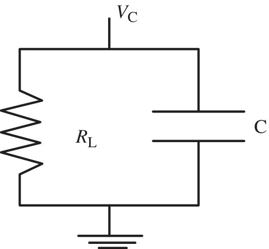
Figure 7.2 Capacitor leakage model
The total excess charging at the base is due to surface and bulk leakage
This indicates that as the transistor ages, Qbe increases along with Ib. Some of the increase in Qbe is caused by the increase in impurities and defects in the base surface and bulk regions due to operating stress.
The impurities and defects cause an increase in electron scattering and an increase in the probability for trapping and charging and eventual recombination in the base. The above feature leads to an increased leakage current. In the capacitive model shown in Figure 7.2, incremental changes are
where we view Q, V, and I as time-varying with age, that is,
Thus, a second result is that the change in β is proportional to the fractional change in the base-emitter leakage current, charge, and voltage.
Experimentally, β degradation is observed to follow a logarithmic-in-time aging as exemplified in Figure 7.3. Data plotted on C-doped MBEHBT device at 235°C at 10 kA/cm2 are shown in Figure 7.3 [4]:

Figure 7.3 Beta degradation on life test data.
Source: Feinberg et al. [4]. Reproduced with permission of IEST
7.4.3 Thermally Activated Time-Dependent Model for Transistors and Dielectric Leakage
The leakage current often leading to dielectric breakdown has historically been explored and there are numerous mechanisms, or a combination of several, providing a physical explanation of the origin of the current that flows through the dielectric. These models stem from the fact that the work required to create defects that increase leakage current is thermally activated, and there is a reduction in the free energy barrier for defect generation due to the electric field lowering the barrier for defect creation. For example, in a bond breakage model, the E-field relates to the bonds breakage through the dipole energy. The energy barrier for creating defects has the form
We identify that the change in the free energy is due to damage that occurred from electrical thermodynamic conjugate work (see Table 1.1):
Common dielectric leakage mechanisms that relate to various forms of the free energy with different explanations include the: Poole–Frenkel effect; Schottky effect; thermo-chemical E-model; tunneling; and Fowler–Nordheim tunneling. The most general expression for current density j for these models is

where E is the electric field and α and C are constants. For the Poole–Frenkel [5] model K = 1, N = 1/2; for the Schottky effect [6] model K = 0, N = 1/2; for the thermo-chemical model K = 0, N = 1; and for the tunneling models K = 2, N = −1 [6].
We can start our leakage TAT model consistent with Equation (7.28) and use Equations (7.26) and (7.27) for the free energy with N = 1 and the general constant K as

This is in the form of the TAT model results (see Equations (6.7) and (6.8)) where we find
where

Alternatively,

and

We expect K > 0 for Beta degradation ![]() to increase with
to increase with ![]() . The result of this logarithmic-in-time model yields a good fit to the beta degradation data in Figure 7.3 and for the FET data in Figure 7.4.
. The result of this logarithmic-in-time model yields a good fit to the beta degradation data in Figure 7.3 and for the FET data in Figure 7.4.

Figure 7.4 Life test data of gate-source MESFET leakage current over time fitted to the ln(1 + Bt) aging model. Junction rise was about 30°C.
Source: Feinberg et al. [4]. Reproduced with permission of IEST
7.4.4 Field-Effect Transistor Parameter Degradation
In this section, transconductance degradation over time is described to help understand aging in FET devices such as MESFETs. Unlike the beta parameter for the bipolar case, we note that transconductance can also apply to bipolar or FET devices. This methodology applied to FETs can also be extended to the bipolar case. The transconductance in the FET case is of interest as a small change in the gate-source voltage Vgs can make a large change in the current flowing out of the drain Ids of the device. The transconductance gm relates these two variables as ![]() . It is this amplification factor that we will now be concerned about for degradation issues.
. It is this amplification factor that we will now be concerned about for degradation issues.
A key issue similar to bipolar transistor degradation in FET type devices is again leakage current [4].
We start by modeling a change in the transconductance gm similar to beta change as
where the initial value g0 is taken from the linear portion of the transconductance curve, that is
Here, we use the linear portion of the curve for simplicity. Similar results will follow for other portions of the curve. The time-dependent function Δgm(t) is found from its derivative as:

or

We assume that the drain-source current change occurs as ![]() with Vds constant and voltage-gate change as
with Vds constant and voltage-gate change as ![]() . Approximating d/dt by Δ/Δt and noting that Δt is common to both sides of the equation and canceling, the expression simplifies to
. Approximating d/dt by Δ/Δt and noting that Δt is common to both sides of the equation and canceling, the expression simplifies to

Thus, the primary result for FETs is that transconductance aging arises from a change in the drain-source resistance and gate leakage. However, it is commonly found that resistance aging dominates the reaction [4]. As far as Rds is concerned, resistance is related to scattering inside the drain-source channel ![]() , where ρ is the resistivity, and l is the average mean-free path traveled by the electrons in the channel between collisions. This distance decreases as aging occurs and more defects occur in the channel, causing increased scattering.
, where ρ is the resistivity, and l is the average mean-free path traveled by the electrons in the channel between collisions. This distance decreases as aging occurs and more defects occur in the channel, causing increased scattering.
At this point, we wish to point out that MESFET gate leakage aging data as shown commonly follows a logarithmic-in-time aging form similar to β degradation (a mechanism that we have modeled as dominated by leakage). This aging time dependence is illustrated in the life test data in Figure 7.4 over two aging temperatures [4]. The TAT model for gate leakage, similar to Equation (7.31) is

where

This model is found to nicely fit the life test data in Figure 7.4.
References
- [1] Kato, K. and Adachi, K. (2001) Wear mechanisms, in Modern Tribology Handbook (ed B. Bhushan), CRC Press, Boca Raton.
- [2] Chiou, Y.C., Kato, K. and Kayaba, T. (1985) Effect of normal stiffness in loading system on wear of carbon steel—part 1: severe-mild wear transition. Journal of Tribology, 107, 491–495.
- [3] Lubliner, J. (2008see Chapter 2) Plasticity Theory, Dover Publications, Mineola.
- [4] Feinberg, A., Ersland, P., Kaper, V. and Widom, A. (2000) On aging of key transistor device parameters. Proceedings: Institute of Environmental Sciences and Technology, 46, 231.
- [5] Harrell, W.R. and Frey, J. (1999) Observation of Poole–Frenkel effect saturation in SiO2 and other insulating films. Thin Solid Films, 352, 195–204.
- [6] Sze, S.M. (1981) Physics of Semiconductor Devices, John Wiley & Sons, Inc., New York.