Power electronic converters for motor drives
Abstract
Power electronics allows us to vary the supply voltage and/or frequency to a motor, and thereby greatly extend and enhance its already remarkable performance. The operation of all the most important types of converter is covered, and the key features, switching strategies, and characteristics of all types are identified. The introductory level treatment will suit readers with no prior knowledge of the subject.
Keywords
Power electronic; Motor drive; Power semiconductor; Converter; Inverter; PWM; Voltage control; Frequency control
2.1 Introduction
In this chapter we look at the power converter circuits which are widely used with motor drives, providing either d.c. or a.c. outputs, and working from either a d.c. (e.g. battery) supply, or from the conventional (50 or 60 Hz) utility supply. All of the principal converter types are introduced, but the coverage is not intended to be exhaustive, with attention being concentrated on the most important topologies, their features and aspects of behaviour which recur in many types of drive converter.
All except very low power converters are today based on power electronic switching. The need to adopt a switching strategy is emphasised in the first example, where the consequences are explored in some depth. We will see that switching is essential in order to achieve high-efficiency power conversion, but that the resulting waveforms are inevitably less than ideal from the point of view of both the motor and the power supply.
The examples have been chosen to illustrate typical practice, so the most commonly used switching devices (e.g. thyristor, MOSFET, and IGBT) are shown. In many cases, several different switching devices may be suitable (see later), so we should not identify a particular circuit as being the exclusive preserve of a particular device.
Power semiconductor devices are the subject of continuous innovation, with faster switching, lower on-state resistance, higher operating temperatures, higher blocking voltage capability, improved robustness to fault conditions and of course cost/competitive advantage being the main drivers. These developments rarely impact on either the topology of power converters or their principal characteristics, and so detailed review of power semiconductor switches is beyond the scope of this book.1
This chapter covers all the most significant types of power converter circuits used in d.c. and a.c. drives. There are a small number of further topologies which are specific to the control of a particular motor type, and these will be discussed when we come to look at those motors.
Before discussing particular circuits it will be useful to take an overall look at a typical drive system, so that the role of the converter can be seen in its proper context.
2.1.1 General arrangement of drive
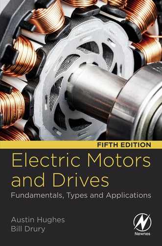
A complete drive system is shown in block diagram form in Fig. 2.1.
The job of the power converter is to draw electrical energy from the utility supply (at constant voltage and frequency) and supply electrical energy to the motor at whatever voltage and frequency is necessary to achieve the desired mechanical output. In Fig. 2.1, the ‘demanded’ output is the speed of the motor, but equally it could be the torque, the position of the motor shaft, or some other system variable.
Except in the very simplest converter (such as a basic diode rectifier), there are usually two distinct parts to the converter. The first is the power stage, through which the energy flows to the motor, and the second is the control section, which regulates the power flow. Low-power control signals tell the converter what it is supposed to be doing, while other low-power feedback signals are used to measure what is actually happening. By comparing the demand and feedback signals, and adjusting the output accordingly, the target output is maintained.
The basic arrangement shown in Fig. 2.1 is clearly a speed control system, because the signal representing the demand or reference quantity is speed, and we note that it is a ‘closed-loop’ system because the quantity that is to be controlled is measured and fed back to the controller so that action can be taken if they do not correspond. All drives employ some form of closed-loop (feedback) control, so readers who are unfamiliar with the basic principles will probably be well advised to do some background reading.2
In later chapters we will explore the internal workings and control arrangements at greater length, but it is worth mentioning that almost all drives employ current feedback, not only to facilitate over-current protection circuits, but in order to control the motor torque, and that in all except high-performance drives it is unusual to find external transducers, which can account for a significant fraction of the total cost of the drive system. Instead of measuring the actual speed using, for example, a shaft-mounted tachogenerator as shown in Fig. 2.1, speed is more likely to be derived from sampled measurements of motor voltages, currents, and frequency, used in conjunction with a stored mathematical model of the motor.
A characteristic of power electronic converters, which is shared with most electrical systems, is that they usually have very little capacity for storing energy. This means that any sudden change in the power supplied by the converter to the motor must be reflected in a sudden increase in the power drawn from the supply. In most cases this is not a serious problem, but it does have two drawbacks. Firstly, sudden increases in the current drawn from the supply will cause momentary drops in the supply voltage, because of the effect of the supply impedance. These voltage ‘dips’ will appear as unwelcome distortion to other users on the same supply. And secondly, there may be an enforced delay before the supply can furnish extra power. For example, with a single-phase utility supply, there can be no sudden increase in the power supply at the instant where the utility voltage is zero, because instantaneous power is necessarily zero at this point in the cycle because the voltage is itself zero.
It would be ideal if the converter could store at least enough energy to supply the motor for several cycles of the 50/60 Hz supply, so that short-term energy demands could be met instantly, thereby reducing rapid fluctuations in the power drawn from the utility supply. But unfortunately this is rarely economic: most converters do have a small store of energy in their smoothing inductors and capacitors, but the amount is not sufficient to buffer the supply sufficiently to shield it from anything more than very short-term fluctuations.
2.2 Voltage control—D.C. output from d.c. supply
In Chapter 1 we saw that control of the basic d.c. machine is achieved by controlling the current in the conductor, which is readily achieved by variation of the voltage. A controllable voltage source is therefore a key element of a motor drive, as we will see in later chapters.
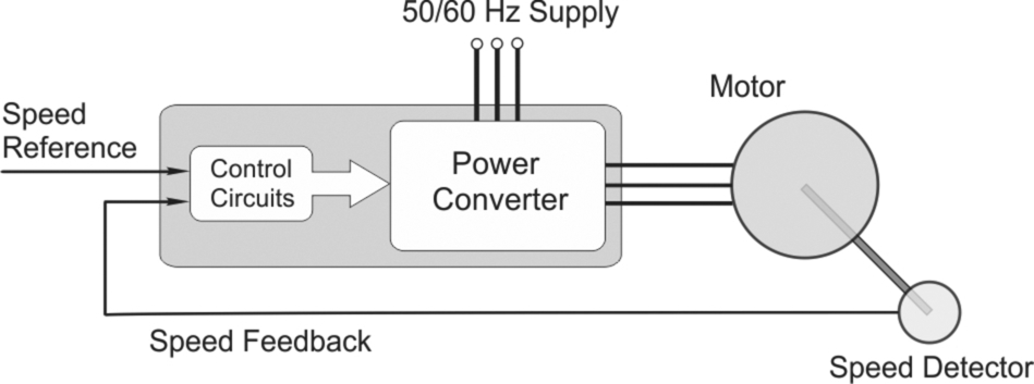
However, for the sake of simplicity we will begin by exploring the problem of controlling the voltage across a 2 Ω resistive load, fed from a 12 V constant-voltage source such as a battery. Three different methods are shown in Fig. 2.2, in which the circle on the left represents an ideal 12 V d.c. source, the tip of the arrow indicating the positive terminal. Although this set-up is not quite the same as if the load was a d.c. motor the conclusions which we draw are more or less the same.
Method (A) uses a variable resistor (R) to absorb whatever fraction of the battery voltage is not required at the load. It provides smooth (albeit manual) control over the full range from 0 to 12 V, but the snag is that power is wasted in the control resistor. For example, if the load voltage is to be reduced to 6 V, the resistor R must be set to 2 Ω, so that half of the battery voltage is dropped across R. The current will be 3 A, the load power will be 18 W, and the power dissipated in R will also be 18 W. In terms of overall power conversion efficiency (i.e. useful power delivered to the load divided by total power from the source) the efficiency is a very poor 50%. If R is increased further, the efficiency falls still lower, approaching zero as the load voltage tends to zero. Whilst this method of control was commonplace before the advent of power semiconductors in the 1960s, and some examples will still be seen in use, the cost of energy, cooling and safety considerations have led to its demise, except perhaps in applications such as low cost, low power hand tools and toy racing cars.
Method (B) is much the same as (A) except that a transistor is used instead of a manually-operated variable resistor. The transistor in Fig. 2.2B is connected with its collector and emitter terminals in series with the voltage source and the load resistor. The transistor is a variable resistor, of course, but a rather special one in which the effective collector-emitter resistance can be controlled over a wide range by means of the base-emitter current. The base-emitter current is usually very small, so it can be varied by means of a low-power electronic circuit (not shown in Fig. 2.2) whose losses are negligible in comparison with the power in the main (collector-emitter) circuit.
Method (B) shares the drawback of method (A) above, i.e. the efficiency is very low. But even more seriously, the ‘wasted’ power (up to a maximum of 18 W in this case) is burned-off inside the transistor, which therefore has to be large, well-cooled, and hence expensive. Transistors are almost never operated in this ‘linear’ way when used in power electronics, but are widely used as ON/OFF switches, as discussed below.
2.2.1 Switching control
The basic ideas underlying a switching power regulator are shown by the arrangement in Fig. 2.2C, which uses a mechanical switch. By operating the switch repetitively and varying the ratio of ON to OFF time, the average load voltage can be varied continuously between 0 V (switch OFF all the time) through 6 V (switch ON and OFF for half of each cycle) to 12 V (switch ON all the time).
The circuit shown in Fig. 2.2C is often referred to as a ‘chopper’, because the d.c. battery supply is ‘chopped’ ON and OFF. A constant repetition frequency (switching frequency) is normally used, and the width of the ON pulse is varied to control the mean output voltage (see the waveform in Fig. 2.2): this is known as ‘pulse width modulation’ (PWM).
The main advantage of the chopper circuit is that no power is wasted, and the efficiency is thus 100%. When the switch is ON, current flows through it, but the voltage across it is zero because its resistance is negligible. The power dissipated in the switch is therefore zero. Likewise, when OFF the current through it is zero, so although the voltage across the switch is 12 V, the power dissipated in it is again zero.
The obvious disadvantage is that by no stretch of the imagination could the load voltage be seen as ‘good’ d.c.: instead it consists of a mean or ‘d.c.’ level, with a superimposed ‘a.c.’ component. Bearing in mind that we really want the load to be a d.c. motor, rather than a resistor, we are bound to ask whether the pulsating voltage will be acceptable. Fortunately, the answer is yes, provided that the chopping frequency is high enough. We will see later that the inductance of the motor causes the current to be much smoother than the voltage, which means that the motor torque fluctuates much less than we might suppose; and the mechanical inertia of the motor filters the torque ripples so that the speed remains almost constant, at a value governed by the mean (or d.c.) level of the chopped waveform.
Obviously a mechanical switch would be unsuitable, and could not be expected to last long when pulsed at high frequency. So a power electronic switch is used instead. The first of many devices to be used for switching was the bipolar junction transistor (BJT), so we will begin by examining how such devices are employed in chopper circuits. If we choose a different device, such as a metal oxide semiconductor field effect transistor (MOSFET) or an insulated gate bipolar transistor (IGBT), where the gate drive circuits are simpler and lower power, the main conclusions we draw will be much the same.
2.2.2 Transistor chopper
As noted earlier, a transistor is effectively a controllable resistor, i.e. the resistance between collector and emitter depends on the current in the base-emitter junction. In order to mimic the operation of a mechanical switch, the transistor would have to be able to provide infinite resistance (corresponding to an open switch) or zero resistance (corresponding to a closed switch). Neither of these ideal states can be reached with a real transistor, but both can be approximated closely.
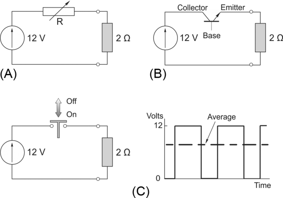
The typical relationship between the collector-emitter voltage and the collector current for a range of base currents rising from zero is shown in Fig. 2.3. The bulk of the diagram represents the so-called ‘linear’ region, where the transistor exhibits the remarkable property of the collector current remaining more or less constant for a wide range of collector-emitter voltages: when the transistor operates in this region there will be significant power loss. For power electronic applications, we want the device to behave like a switch, so we operate on the margins of the diagram, where either the voltage or the current is close to zero, and the heat released inside the device is therefore very low.
The transistor will be OFF when the base-emitter current (Ib) is zero. Viewed from the main (collector-emitter) circuit, its resistance will be very high, as shown by the region Oa in Fig. 2.3.
Under this ‘cut-off’ condition, only a tiny current (Ic) can flow from the collector to the emitter, regardless of the voltage (Vce) between the collector and emitter. The power dissipated in the device will therefore be minimal, giving an excellent approximation to an open switch.
To turn the transistor fully ON, a base-emitter current must be provided. The base current required will depend on the prospective collector-emitter current, i.e. the current in the load. The aim is to keep the transistor ‘saturated’ so that it has a very low resistance, corresponding to the region Ob in Fig. 2.3. In the example shown in Fig. 2.2, if the resistance of the transistor is very low, the current in the circuit will be almost 6 A, so we must make sure that the base-emitter current is sufficiently large to ensure that the transistor remains in the saturated condition when Ic = 6 A.
Typically in a bipolar transistor (BJT) the base current will need to be around 5–10% of the collector current to keep the transistor in the saturation region: in the example (Fig. 2.2), with the full load current of 6 A flowing, the base current might be 400 mA, the collector-emitter voltage might be say 0.33 V, giving an on-state dissipation of 2 W in the transistor when the load power is very nearly 72 W. The power conversion efficiency is not 100%, as it would be with an ideal switch, but it is acceptable.
We should note that the on-state base-emitter voltage is very low, which, coupled with the small base current, means that the power required to drive the transistor is very much less than the power being switched in the collector-emitter circuit. Nevertheless, to switch the transistor in the regular pattern shown in Fig. 2.2, we obviously need a base current which goes on and off periodically, and we might wonder how we obtain this ‘control’ signal. In most modern drives the signal originates from a microprocessor, many of which are designed with PWM auxiliary functions, which can be used for this purpose. Depending on the base circuit current requirements of the main switching transistor, it may be possible to feed it directly from the microprocessor, but it is more usual to see additional transistors interposed between the signal source and the main device to provide the required power amplification.
Just as we have to select mechanical switches with regard to their duty, we must be careful to use the right power transistor for the job in hand. In particular, we need to ensure that when the transistor is ON, we don’t exceed the safe current, or else the active semiconductor region of the device will be destroyed by overheating. And we must make sure that the transistor is able to withstand whatever voltage appears across the collector-emitter junction when it is in the OFF condition. If the safe voltage is exceeded, even for a very short period, the transistor will breakdown, and be permanently ON.
A suitable heatsink will be a necessity in all but the smallest and most efficient drives. We have already seen that some heat is generated when the transistor is ON, and at low switching rates this is the main source of unwanted heat. But at high switching rates, ‘switching loss’ can also be very important.
Switching loss is the heat generated in the finite time it takes for the transistor to go from ON to OFF or vice-versa. The base-drive circuitry will be arranged so that the switching takes place as fast as possible, but in practice, with silicon-based power semiconductors, it will seldom take less than a few microseconds. During the switch-on period, for example, the current will be building up, while the collector-emitter voltage will be falling towards zero. The peak power reached can therefore be large, before falling to the relatively low on-state value. Of course the total energy released as heat each time the device switches is modest because the whole process happens so quickly. Hence if the switching rate is low (say once every second) the switching power loss will be insignificant in comparison with the on-state power. But at high switching rates, when the time taken to complete the switching becomes comparable with the ON time, the switching power loss can easily become dominant. In drives, switching rates vary somewhat depending upon the power rating. In general, the higher the power the lower the switching frequency. Many commercial drives allow the user to select the switching frequency, but by selecting high switching frequencies to give smoother current waveforms (and lower audible noise) the higher losses mean that the rating of the drive must be reduced. New, so called Wide Band Gap (WBG) power devices, notably Gallium Nitride and Silicon Carbide are now available which offer the prospect of much faster switching times, and therefore much lower switching losses, than is possible with silicon. Such devices allow efficient switching frequencies into the MHz region, and will become more prevalent in future as their costs fall.
2.2.3 Chopper with inductive load—Overvoltage protection
So far we have looked at chopper control of a resistive load, but in a drives context the load will usually mean the winding of a machine, which will invariably be inductive.
Chopper control of inductive loads is much the same as for resistive loads, but we have to be careful to prevent the appearance of dangerously high voltages each time the inductive load is switched OFF. The root of the problem lies with the energy stored in the magnetic field of the inductor. When an inductance L carries a current I, the energy stored in the magnetic field (W) is given by

If the inductor is supplied via a mechanical switch, and we open the switch with the intention of reducing the current to zero instantaneously, we are in effect seeking to destroy the stored energy. This is not possible (because it would imply an energy pulse of zero duration and hence infinite power), and what happens instead is that the energy is dissipated in the form of a spark (or arc) across the contacts of the switch.
The appearance of a spark indicates that there is a very high voltage, sufficient to break down the surrounding air. We can anticipate this by remembering that the voltage and current in an inductance are related by the equation

which shows that the self-induced voltage is proportional to the rate of change of current, so when we open the switch in order to force the current to zero quickly, a very large voltage is created in the inductance. This voltage appears across the terminals of the switch and, if sufficient to break down the air, the resulting arc allows the current to continue to flow until the stored magnetic energy is dissipated as heat in the arc.
Sparking across a mechanical switch is unlikely to cause immediate destruction, but when a transistor is used its immediate demise is certain unless steps are taken to tame the stored energy, and in particular ensure that the voltage seen by the transistor does not exceed its rated peak voltage. The usual remedy lies in the use of a ‘freewheel diode’ (sometimes called a flywheel diode), as shown in Fig. 2.4.

A diode is a one-way valve as far as current is concerned: it offers very little resistance to current flowing from anode to cathode (i.e. in the direction of the broad arrow in the symbol for a diode), but blocks current flow from cathode to anode. Actually, when a power diode conducts in the forward direction, the voltage drop across it is usually not all that dependent on the current flowing through it, so the reference above to the diode ‘offering little resistance’ is not strictly accurate because it does not obey Ohm’s law. In practice the volt-drop of power diodes (most of which are made from silicon) is around 0.7 V, regardless of the current rating.
In the circuit of Fig. 2.4A, when the transistor is ON, current (I) flows through the load, but not through the diode, which is said to be reverse-biased (i.e. the applied voltage is trying—unsuccessfully—to push current down through the diode). During this period the voltage across the inductance is positive, so the current increases, thereby increasing the stored energy.
When the transistor is turned OFF, the current through it and the battery drops very quickly to zero. But the stored energy in the inductance means that its current cannot suddenly disappear. So since there is no longer a path through the transistor, the current diverts into the only other route available, and flows upwards through the low-resistance path offered by the diode, as shown in Fig. 2.4B.
Obviously the current no longer has a battery to drive it, so it cannot continue to flow indefinitely. During this period the voltage across the inductance is negative, and the current reduces. If the transistor were left OFF for a long period, the current would continue to ‘freewheel’ only until the energy originally stored in the inductance is dissipated as heat, mainly in the load resistance but also in the diode’s own (low) resistance. In normal chopping, however, the cycle restarts long before the current has fallen to zero, giving a current waveform as shown in Fig. 2.4C. Note that the current rises and falls exponentially with a time-constant of L/R, though it never reaches anywhere near its steady-state value in Fig. 2.4. The sketch corresponds to the case where the time-constant is much longer than one switching period, in which case the current becomes almost smooth, with only a small ripple. In a d.c. motor drive this is just what we want, since any fluctuation in the current gives rise to torque pulsations and consequent mechanical vibrations. (The current waveform that would be obtained with no inductance is also shown in Fig. 2.4: the mean current is the same but the rectangular current waveform is clearly much less desirable, given that ideally we would like constant d.c.).
The freewheel (or flywheel) diode was introduced to prevent dangerously high voltages from appearing across the transistor when it switches off an inductive load, so we should check that this has been achieved. When the diode conducts the forward-bias volt-drop across it is small—typically 0.7 Volts. Hence while the current is freewheeling, the voltage at the collector of the transistor is only 0.7 V above the battery voltage. This ‘clamping’ action therefore limits the voltage across the transistor to a safe value, and allows inductive loads to be switched without damage to the switching element.
We should acknowledge that in this example the discussion has focused on steady-state operation, when the current at the end of every cycle is the same, and it never falls to zero. We have therefore sidestepped the more complex matter of how we get from start-up to the steady state, and we have also ignored the so-called ‘discontinuous current’ mode, when the current in the load does fall to zero during the OFF period. We will touch on the significant consequences of discontinuous operation in drives in later chapters.
We can draw some important conclusions which are valid for all power electronic converters from this simple example. Firstly, efficient control of voltage (and hence power) is only feasible if a switching strategy is adopted. The load is alternately connected and disconnected from the supply by means of an electronic switch, and any average voltage up to the supply voltage can be obtained by varying the mark/space (ON/OFF) ratio. Secondly, the output voltage is not smooth d.c., but contains unwanted a.c. components which, though undesirable, are tolerable in motor drives. And finally, the load current waveform will be smoother than the voltage waveform if—as is the case with motor windings—the load is inductive.
2.2.4 Boost converter
The previous section dealt with the so-called step-down or buck converter, which provides an output voltage less than the input. However, if the motor voltage is higher than the supply (for example in an electric vehicle with a 240 V motor driven from a 48 V battery), a step-up or boost converter is required. Intuitively this seems a tougher challenge altogether, and we might expect to have to first convert the d.c. to a.c. so that a transformer could be used, but in fact the basic principle of transferring ‘packets’ of energy to a higher voltage is very simple and elegant, using the circuit shown in Fig. 2.5. Operation of this circuit is worth discussing because it again illustrates features common to many power electronic converters.

As is usual, the converter operates repetitively at a rate determined by the frequency of switching ON and OFF the transistor (T). During the ON period (Fig. 2.5A), the input voltage (Vin) is applied across the inductor (L), causing the current in the inductor to rise linearly, thereby increasing the energy stored in its magnetic field. Meanwhile, the motor current is supplied by the storage capacitor (C), the voltage of which falls only a little during this discharge period. In Fig. 2.5A, the input current is drawn to appear larger than the output (motor) current, for reasons that will soon become apparent. Recalling that the aim is to produce an output voltage greater than the input, it should be clear that the voltage across the diode (D) is negative (i.e. the potential is higher on the right than on the left in Fig. 2.5), so the diode does not conduct and the input and output circuits are effectively isolated from each other.
When the transistor turns OFF, the current through it falls rapidly to zero, and the situation is much the same as in the step-down converter where we saw that because of the stored energy in the inductor, any attempt to reduce its current results in a self-induced voltage trying to keep the current going. So during the OFF period, the inductor voltage rises extremely rapidly until the potential at the left side of the diode is slightly greater than Vout, the diode then conducts and the inductor current flows into the parallel circuit consisting of the capacitor (C) and the motor, the latter continuing to draw a steady current (as the voltage across the large storage capacitor and hence motor cannot change instantaneously), while the major share of the inductor current goes to recharge the capacitor. The resulting voltage across the inductor is negative, and of magnitude Vout − Vin, so the inductor current begins to reduce and the extra energy that was stored in the inductor during the ON time is transferred into the capacitor. Assuming that we are in the steady-state (i.e. power is being supplied to the motor at a constant voltage and current), the capacitor voltage will return to its starting value at the start of the next ON time.
If the losses in the transistor and the storage elements are neglected, it is easy to show that the converter functions like an ideal transformer, with output power equal to input power, i.e.

We know that the motor voltage Vout is higher than Vin, so not surprisingly the quid pro quo is that the motor current is less than the input current, as indicated by line thickness in Fig. 2.5.
Also if the capacitor is large enough to hold the output voltage very nearly constant throughout, it is easy to show that the step-up ratio is given by

where D is the duty ratio, i.e. the proportion of each cycle for which the transistor is ON. Thus for the example at the beginning of this section, where Vout/Vin = 240/48 = 5, the duty ratio is 0.8, i.e. the transistor has to be ON for 80% of each cycle.
The advantage of switching at a high frequency becomes clear when we recall that the capacitor has to store enough energy to supply the output during the ON period, so if, as is often the case, we want the output voltage to remain almost constant, it should be clear that the capacitor must store a good deal more energy than it gives out each cycle. Given that the size and cost of capacitors depends on the energy they have to store, it is clearly better to supply small packets of energy at a high rate, rather than use a lower frequency that requires more energy to be stored. Conversely, the switching and other losses increase with frequency, so a compromise is inevitable.
2.3 D.C. from a.c.—Controlled rectification
The majority of drives of all types draw their power from a constant voltage 50 Hz or 60 Hz utility supply, and so in many drive converters the first stage consists of a rectifier which converts the a.c. to a crude form of d.c. Where a constant-voltage (i.e. unvarying average) ‘d.c.’ output is required, a simple (uncontrolled) diode rectifier is usually sufficient. But where the mean d.c. voltage has to be controllable (as in a d.c. motor drive to obtain varying speeds), a controlled rectifier is used.
Many different converter configurations based on combinations of diodes and thyristors are possible, but we will focus on ‘fully-controlled’ converters in which all the rectifying devices are thyristors, because they are predominant in modern motor drives. Half-controlled converters are used less frequently, so will not be covered here.
From the user’s viewpoint, interest centres on the following questions:
- • How is the output voltage controlled?
- • What does the converter output voltage look like? Will there be any problems if the voltage is not pure d.c.?
- • How does the range of the output voltage relate to the a.c. supply voltage?
- • How is the converter and motor drive ‘seen’ by the supply system? What is the power factor, and is there distortion of the supply voltage waveform, with consequent interference to other users?
We can answer these questions without going too thoroughly into the detailed workings of the converter. This is just as well, because understanding all the ins and outs of converter operation is beyond our scope. On the other hand it is well worth studying the essence of the controlled rectification process, because it assists in understanding the limitations which the converter puts on drive performance (see Chapter 4, etc.). Before tackling the questions posed above, however, it is obviously necessary to introduce the thyristor.
2.3.1 The thyristor
The thyristor is a power electronic switch, with two main terminals (anode and cathode) and a ‘switch-on’ terminal (gate), as shown in Fig. 2.6.

Like a diode, current can only flow in the forward direction, from anode to cathode. But unlike a diode, which will conduct in the forward direction as soon as forward voltage is applied, the thyristor will continue to block forward current until a small current pulse is injected into the gate-cathode circuit, to turn it ON or ‘fire’ it. After the gate pulse is applied, the main anode-cathode current builds up rapidly, and as soon as it reaches the ‘latching’ level, the gate pulse can be removed and the device will remain ON.
Once established, the anode-cathode current cannot be interrupted by any gate signal. The non-conducting state can only be restored after the anode-cathode current has reduced to zero, and has remained at zero for the turn-off time (typically 100–200 μs).
When a thyristor is conducting it approximates to a closed switch, with a forward drop of only one or two volts over a wide range of current. Despite the low volt drop in the ON state, heat is dissipated, and heatsinks must usually be provided, perhaps with fan or other forms of cooling. Devices must be selected with regard to the voltages to be blocked and the r.m.s. and peak currents to be carried. Their overcurrent capability is very limited, and it is usual in drives for devices to have to withstand perhaps twice full-load current for a few seconds only, though this is dependent on the application. Special fuses must be fitted to protect against large fault currents.
The reader may be wondering why we need the thyristor, since in the previous section we discussed how a transistor could be used as an electronic switch. On the face of it the transistor appears even better than the thyristor because it can be switched OFF while the current is flowing, whereas the thyristor will remain ON until the current through it has been reduced to zero by external means. The primary reason for the use of thyristors is that they are cheaper and their voltage and current ratings extend to higher levels than in power transistors. In addition, the circuit configuration in rectifiers is such that there is no need for the thyristor to be able to interrupt the flow of current, so its inability to do so is no disadvantage. Of course there are other circuits (see for example the next section dealing with inverters) where the devices need to be able to switch OFF on demand, in which case the transistor then has the edge over the thyristor.
2.3.2 Single pulse rectifier
The simplest phase-controlled rectifier circuit is shown in Fig. 2.7. When the supply voltage is positive, the thyristor blocks forward current until the gate pulse arrives, and up to this point the voltage across the resistive load is zero. As soon as a firing pulse is delivered to the gate-cathode circuit (not shown in Fig. 2.7) the device turns ON, the voltage across it falls to near zero, and the load voltage becomes equal to the supply voltage. When the supply voltage reaches zero, so does the current. At this point the thyristor regains its blocking ability, and no current flows during the negative half-cycle.
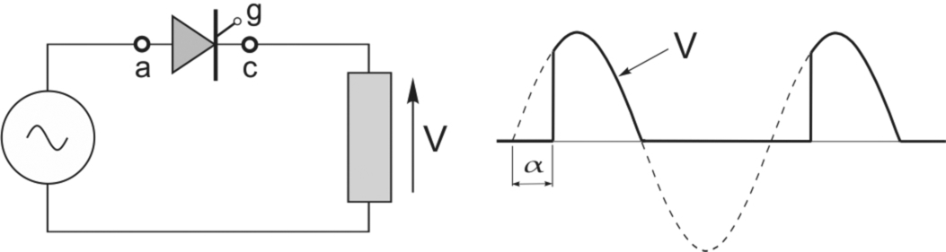
If we neglect the small on-state volt-drop across the thyristor, the load voltage (Fig. 2.7) will consists of part of the positive half-cycles of the a.c. supply voltage. It is obviously not smooth, but is ‘d.c’ in the sense that it has a positive mean value; and by varying the delay angle (α) of the firing pulses the mean voltage can be controlled. With a purely resistive load, the current waveform will simply be a scaled version of the voltage.
This arrangement gives only one peak in the rectified output for each complete cycle of the supply, and is therefore known as a ‘single-pulse’ or half-wave circuit. The output voltage (which ideally we would like to be steady d.c.) is so poor that this circuit is almost never used in drives. Instead, drive converters use four or six thyristors, and produce much superior output waveforms with two or six pulses per cycle, as will be seen in the following sections.
2.3.3 Single-phase fully-controlled converter—Output voltage and control
The main elements of the converter circuit are shown in Fig. 2.8. It comprises four thyristors, connected in bridge formation. (The term bridge stems from early four-arm measuring circuits which presumably suggested a bridge-like structure to their inventors.)
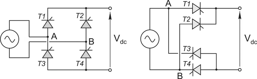
The conventional way of drawing the circuit is shown on the left side in Fig. 2.8, while on the right side it has been redrawn to assist understanding: the load is connected to the output terminals, where the voltage is Vdc. The top of the load can be connected (via T1) to terminal A of the supply, or (via T2) to terminal B of the supply, and likewise the bottom of the load can be connected either to A or to B via T3 or T4 respectively.
We are naturally interested to find what the output voltage waveform on the d.c. side will look like, and in particular to discover how the mean d.c. level can be controlled by varying the firing delay angle α. The angle α is measured from the point on the waveform when a diode in the same circuit position would start to conduct, i.e. when the anode becomes positive with respect to the cathode.
This is not such a simple matter as we might have expected, because it turns out that the mean voltage for a given α depends on the nature of the load. We will therefore look first at the case where the load is resistive, and explore the basic mechanism of phase control. Later, we will see how the converter behaves with a typical inductive motor load.
Resistive load
Thyristors T1 and T4 are fired together when terminal A of the supply is positive, while on the other half-cycle, when B is positive, thyristors T2 and T3 are fired simultaneously. The output voltage and current waveform are shown in Fig. 2.9A and B, respectively, the current simply being a replica of the voltage. There are two pulses per cycle of the supply, hence the description ‘2-pulse’ or full-wave.
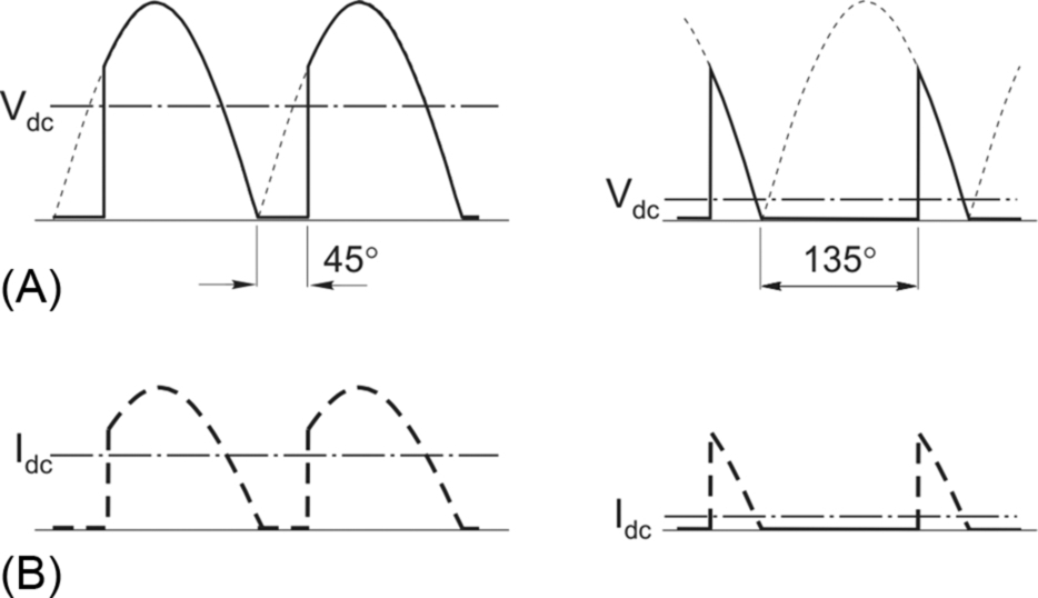
The load is either connected to the supply by the pair of switches T1 and T4, or it is connected the other way up by the pair of switches T2 and T3, or it is disconnected. The load voltage therefore consists of rectified chunks of the incoming supply voltage. It is much smoother than in the single-pulse circuit, though again it is far from pure d.c.
The waveforms in Fig. 2.9A and B correspond to delay angles α = 45° and α = 135° respectively. The mean value, Vdc is shown in each case. It is clear that the larger the delay angle, the lower the output voltage. The maximum output voltage (Vdo) is obtained with α = 0°: this is the same as would be obtained if the thyristors were replaced by diodes, and is given by

where Vrms is the r.m.s. voltage of the incoming supply.
The variation of the mean d.c. voltage with α is given by

from which we see that with a resistive load the d.c. voltage can be varied from a maximum of Vdo down to zero by varying α from 0° to 180°.
Inductive (motor) load
As mentioned above, motor loads are inductive, and we have seen earlier that the current cannot change instantaneously in an inductive load. We must therefore expect the behaviour of the converter with an inductive load to differ from that with a resistive load, in which the current was seen to change instantaneously.
The realisation that the mean voltage for a given firing angle might depend on the nature of the load is a most unwelcome prospect. What we would like is to be able to say that, regardless of the load, we can specify the output voltage waveform once we have fixed the delay angle α. We would then know what value of α to select to achieve any desired mean output voltage. What we find in practice is that once we have fixed α, the mean output voltage with a resistive-inductive load is not the same as with a purely resistive load, and therefore we cannot give a simple general formula for the mean output voltage in terms of α. This is of course very undesirable: if for example we had set the speed of our unloaded d.c. motor to the target value by adjusting the firing angle of the converter to produce the correct mean voltage, the last thing we would want is for the voltage to fall when the load current drawn by the motor increased, as this would cause the speed to fall below the target.
Fortunately however, it turns out that the output voltage waveform for a given α does become independent of the load inductance once there is sufficient inductance to prevent the load current from ever falling to zero. This condition is known as ‘continuous current’; and, happily, many motor circuits do have sufficient self-inductance to ensure that we achieve continuous current. Under continuous current conditions, the output voltage waveform only depends on the firing angle, and not on the actual inductance present. This makes things much more straightforward, and typical output voltage waveforms for this continuous current condition are shown in Fig. 2.10.
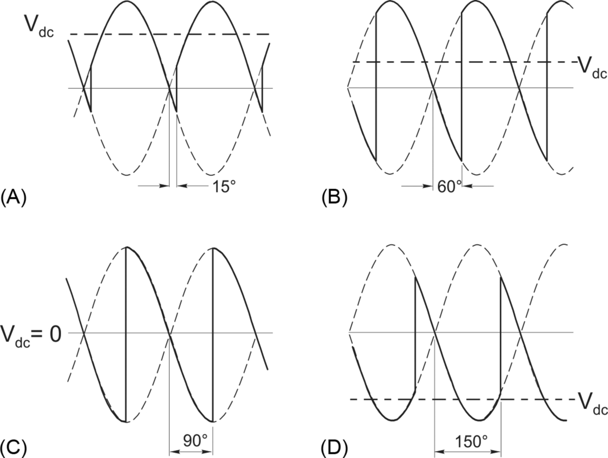
The waveforms in Fig. 2.10 show that, as with the resistive load, the larger the delay angle the lower the mean output voltage. However with the resistive load the output voltage was never negative, whereas we see that, although the mean voltage is positive for values of α below 90° there are brief periods when the output voltage becomes negative. This is because the inductance smoothes out the current (see Fig. 4.2, for example) so that at no time does it fall to zero. As a result, one or other pair of thyristors is always conducting, so at every instant the load is connected directly to the supply, and therefore the load voltage always consists of chunks of the supply voltage.
Rather surprisingly, we see that when α is > 90°, the average voltage is negative (though of course, the current is still positive). The fact that we can obtain a net negative output voltage with an inductive load contrasts sharply with the resistive load case, where the output voltage could never be negative. The combination of negative voltage and positive current means that the power flow is reversed, and energy is fed back to the supply system. We will see later that this facility allows the converter to return energy from the load to the supply, and this is important when we want to use the converter with a d.c. motor in the regenerating mode.
It is not immediately obvious why the current switches (or ‘commutates’) from the first pair of thyristors to the second pair when the latter are fired, so a brief look at the behaviour of diodes in a similar circuit configuration may be helpful at this point. Consider the set-up shown in Fig. 2.11, with two voltage sources (each time-varying) supplying a load via two diodes. The question is what determines which diode conducts, and how does this influence the load voltage?
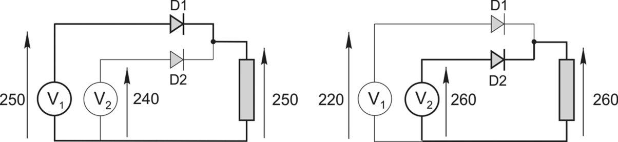
We can consider two instants as shown in the diagram. On the left, V1 is 250 V, V2 is 240 V, and D1 is conducting, as shown by the heavy line. If we ignore the volt-drop across the diode, the load voltage will be 250 V, and the voltage across diode D2 will be 240–250 = − 10 V, i.e. it is reverse biased and hence in the non-conducting state. At some other instant (on the right of the diagram), V1 has fallen to 220 V while V2 has increased to 260 V: now D2 is conducting instead of D1, again shown by the heavy line, and D1 is reverse-biased by − 40 V. The simple pattern is that the diode with the highest anode potential will conduct, and as soon as it does so it automatically reverse-biases its predecessor. In a single-phase diode bridge, for example, the commutation occurs at the point where the supply voltage passes through zero: at this instant the anode voltage on one pair goes from positive to negative, while on the other pair the anode voltage goes from negative to positive.
The situation in controlled thyristor bridges is very similar, except that before a new device can take over conduction, it must not only have a higher anode potential, but it must also receive a firing pulse. This allows the changeover to be delayed beyond the point of natural (diode) commutation by the angle α, as shown in Fig. 2.10. Note that the maximum mean voltage (Vd0) is again obtained when α is zero, and is the same as for the resistive load (Eq. 2.3). It is easy to show that the mean d.c. voltage is now related to α by
This equation indicates that we can control the mean output voltage by controlling α, though Eq. (2.5) shows that the variation of mean voltage with α is different from that for a resistive load (Eq. 2.4), not least because when α is > 90° the mean output voltage is negative.
It is sometimes suggested (particularly by those with a light-current background) that a capacitor could be used to smooth the output voltage, this being common practice in some low-power d.c. supplies. However, the power levels in most d.c. drives are such that in order to store enough energy to smooth the voltage waveform over the half-cycle of the utility supply (20 ms at 50 Hz), very bulky and expensive capacitors would be required. Fortunately, as will be seen later, it is not necessary for the voltage to be smooth as it is the current which directly determines the torque, and as already pointed out the current is always much smoother than the voltage because of inductance.
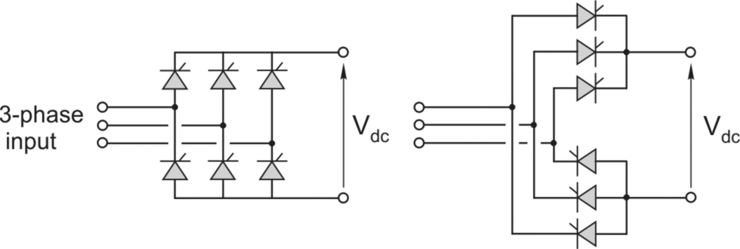
2.3.4 Three-phase fully-controlled converter
The main power elements are shown in Fig. 2.12. The three-phase bridge has only two more thyristors than the single-phase bridge, but the output voltage waveform is vastly better, as shown in Fig. 2.13. There are now six pulses of the output voltage per cycle, hence the description ‘6-pulse’. The thyristors are again fired in pairs (one in the top half of the bridge and one—from a different leg—in the bottom half), and each thyristor carries the output current for one third of the time. As in the single-phase converter, the delay angle controls the output voltage, but now α = 0 corresponds to the point at which the phase voltages are equal (see Fig. 2.13).
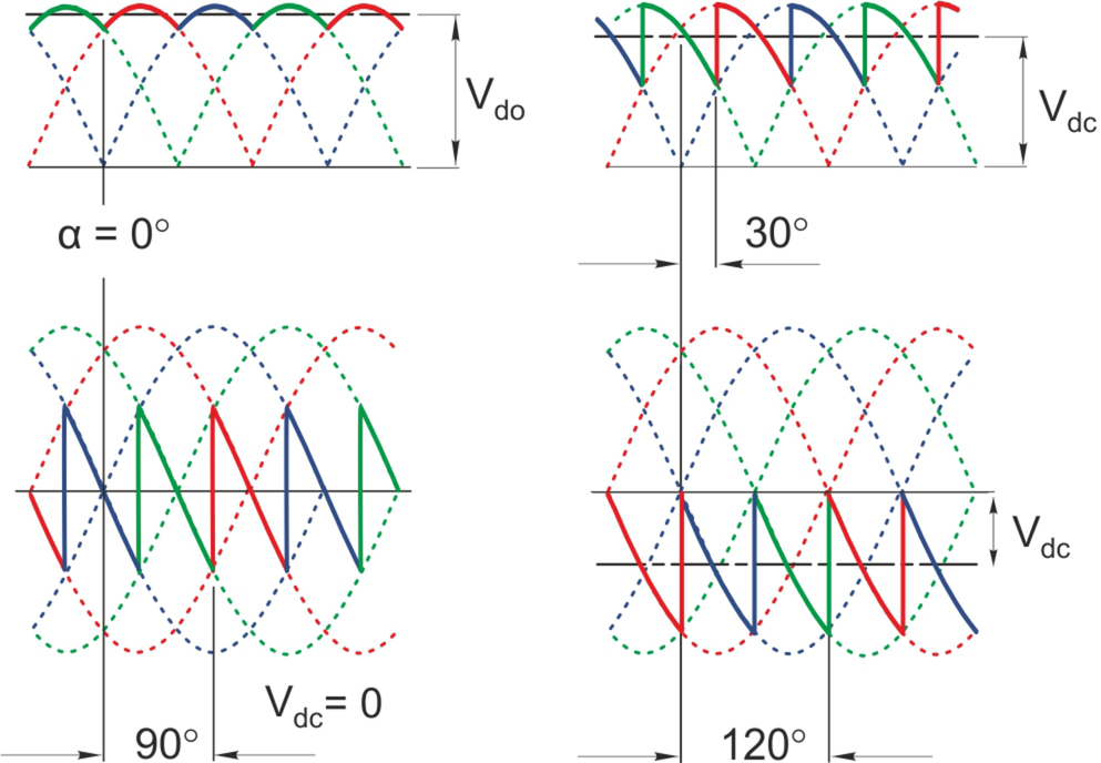
The enormous improvement in the smoothness of the output voltage waveform is clear when we compare Figs. 2.13 and 2.10, and it underlines the benefit of choosing a 3-phase converter whenever possible. The very much better voltage waveform also means that the desirable ‘continuous current’ condition is much more likely to be met, and the waveforms in Fig. 2.13 have therefore been drawn with the assumption that the load current is in fact continuous. Occasionally, even a six-pulse waveform is not sufficiently smooth, and some very large drive converters therefore consist of two six-pulse converters with their outputs in series. A phase-shifting transformer is used to insert a 30° shift between the a.c. supplies to the two 3-phase bridges. The resultant ripple voltage is then 12-pulse.
Readers with prior knowledge of three-phase systems will recall that the three line-line voltages differ in phase by 120°, and they may therefore wonder why the output voltage waveforms in Fig. 2.13 show a transition every 60°, rather than 120° as might be expected. The explanation is simply that the top thyristors switch every 120°, as do the bottom ones, but the transitions are 60° out of step, so there are 6 transitions per cycle.
Returning to the 6-pulse converter, as long as the d.c. current remains continuous, the mean output voltage can be shown to be given by

We note that we can obtain the full range of output voltages from + Vd0 to close to − Vd0, so that, as with the single-phase converter, regenerative operation will be possible.
It is probably a good idea at this point to remind the reader that, in the context of this book, our first application of the controlled rectifier will be to supply a d.c. motor. When we examine the d.c. motor drive in Chapter 4, we will see that it is the average or mean value of the output voltage from the controlled rectifier that determines the speed, and it is this mean voltage that we refer to when we talk of ‘the’ voltage from the converter. We must not forget the unwanted a.c. or ripple element, however, as this can be large. For example, we see from Fig. 2.13 that to obtain a very low d.c. voltage (to make the motor run very slowly) α will be close to 90o; but if we were to connect an a.c. voltmeter to the output terminals it could register several hundred volts, depending on the incoming supply voltage!
2.3.5 Output voltage range
In Chapter 4 we will discuss the use of the fully-controlled converter to drive a d.c. motor, so it is appropriate at this stage to look briefly at the typical voltages we can expect. Utility supply voltages vary, but single-phase supplies are usually 200–240 V, and we see from Eq. (2.3) that the maximum mean d.c. voltage available from a single phase 230 V supply is 207 V. This is suitable for 180–200 V motors. If a higher voltage is needed (for say a 300 V motor), a transformer must be used to step up the incoming supply.
Turning now to typical three-phase supplies, the lowest three-phase industrial voltages are usually around 380–480 V. (Higher voltages of up to 11 kV are used for large drives, but these will not be discussed here). So with Vrms = 400 V for example, the maximum d.c. output voltage (Eq. 2.6) is 540 Volts. After allowances have been made for supply variations and impedance drops, we could not rely on obtaining much more than 500–520 V, and it is usual for the motors used with 6-pulse drives fed from 400 V, 3-phase supplies to be rated in the range 430–500 V. (Often the motor’s field winding will be supplied from single phase 230 V, and field voltage ratings are then around 180–200 V, to allow a margin in hand from the theoretical maximum of 207 V referred to earlier.)
2.3.6 Firing circuits
Since the gate pulses are only of low power, the gate drive circuitry is simple and cheap. Often a single electronic integrated circuit contains all the circuitry for generating the gate pulses, and for synchronising them with the appropriate delay angle α with respect to the supply voltage. To avoid direct electrical connection between the high voltages in the main power circuit and the low voltages used in the control circuits, the gate pulses are coupled to the thyristor either by small pulse transformers, or opto-couplers.
2.4 A.C. from d.c.—Inversion
The business of getting a.c. from d.c. is known as inversion, and nine times out of ten we would ideally like to be able to produce sinusoidal output voltages of whatever frequency and amplitude we choose, to achieve speed control of a.c. motors. Unfortunately the constraints imposed by the necessity to use a switching strategy mean that we always have to settle for a voltage waveform which is composed of ‘chunks’, and is thus far from ideal. Nevertheless it turns out that a.c. motors are remarkably tolerant, and will operate satisfactorily despite the inferior waveforms produced by the inverter.
2.4.1 Single-phase inverter
We can illustrate the basis of inverter operation by considering the single-phase example shown in Fig. 2.14. This inverter uses IGBT’s (see later) as the switching devices, with diodes to provide the freewheel paths needed when the load is inductive.

The input or d.c. side of the inverter (on the left in Fig. 2.14) is usually referred to as the ‘d.c. link’, reflecting the fact that in the majority of cases the d.c. is obtained by rectifying an incoming constant-frequency utility supply as we have discussed earlier. The output or a.c. side is taken from terminals A and B in Fig. 2.14.
When transistors 1 and 4 are switched ON, the load voltage is positive, and equal to the d.c. link voltage, while when 2 and 3 are ON it is negative. If no devices are switched ON, the output/load voltage is zero. These 3 distinct possible output voltage states lead us to describe such an inverter as a 3 level inverter. Typical output voltage waveforms at low and high switching frequencies are shown in Fig. 2.15A and B, respectively.
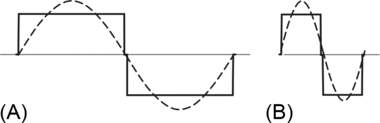
Here each pair of devices is ON for one-half of a cycle. Careful inspection of Fig. 2.15 reveals that there is a very short zero voltage period at the transition point. This is because when switching from one pair of transistors to another it is essential that both transistors in the same arm are never switched ON at the same time as this would provide a short circuit or ‘shoot-through’ path for the d.c. supply: a safety angle is therefore included in the switching logic. The output waveform is clearly not a sine wave, but at least it is alternating and symmetrical. The fundamental component is shown dotted in Fig. 2.15.
We will make frequent references throughout this book to the term ‘fundamental component’, so it is worth a brief digression to explain what it means for any readers who are not familiar with Fourier analysis. In essence, any periodic waveform can be represented as the sum of an infinite series of sinusoidal waves or ‘harmonics’, the frequency of the lowest harmonic (the ‘fundamental’) corresponding to the frequency of the original waveform: Fourier analysis provides the means for calculating the magnitude, phase and order of the harmonic components.
For example, the fundamental, third and fifth harmonics of a square wave are shown in Fig. 2.16.
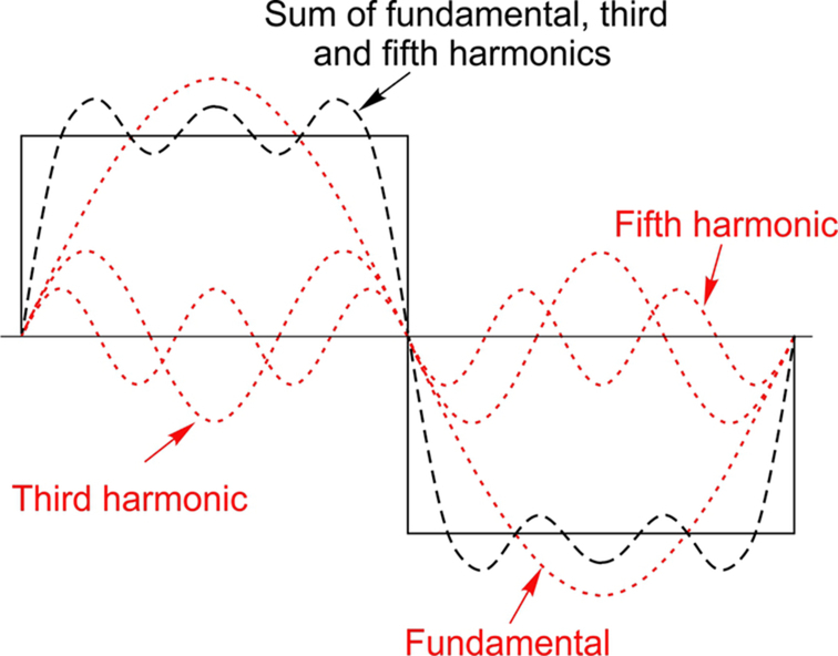
In this particular case, the symmetry of the original waveform is such that only odd harmonics are present, and it turns out that the amplitude of each harmonic is inversely proportional to its order. We can see from Fig. 2.16 that the sum of the fundamental, third and fifth harmonics makes a reasonably good approximation to the original square wave, and if we were to include higher harmonics, the approximation would be even better.
Readers who have studied a.c. circuits under sinusoidal conditions will recall that there are powerful methods based on complex numbers for the steady-state analysis of such circuits, in which inductors and capacitors are represented in terms of their reactances, which depend on the supply frequency. These techniques clearly cannot be applied directly when the waveforms are not sinusoidal, but, because most electrical circuits are linear (i.e. they obey the principle of superposition), we can solve the response to each harmonic separately, and add the responses to determine the final output.
For example, if we want to find the steady-state current in an inductor when a square wave voltage is applied, we find the currents due to the fundamental and each harmonic, and sum the separate currents to obtain the result. Hence the current is given by
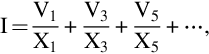
where Xn is the reactance at the nth harmonic frequency.
Recalling that under sinusoidal conditions the reactance of an inductance (L) at frequency f is given by X = 2πfL = ωL, we note that reactance is directly proportional to frequency. Hence if the reactance at the fundamental frequency is X1, the current is given by
It should be clear that for the square wave, where the amplitude of the third harmonic voltage is one third that of the fundamental, the third harmonic current will be only one ninth of the fundamental, and the fifth harmonic current will be only one twenty-fifth. In other words, the current harmonics decrease very rapidly with order, which means that the current waveform is more sinusoidal than the voltage waveform. (In contrast, a resistive load looks the same to each harmonic, so the current waveform is the same as the voltage.)
These conclusions are confirmed by Fig. 2.17, which shows the steady state current waveforms when a square wave of voltage is applied to various loads, the fundamental being shown by the dotted line.

The most noteworthy feature as far as we are concerned is how much smoother the current wave is for the purely inductive case, and how, as a result of its reduced harmonic content, the actual current is closely approximated by the fundamental component. We note also that, as expected, the fundamental current is in phase with the voltage for the resistive load; it lags by 90° for the purely inductive load; and it lies in between for the mixed R-L load.
All this is very fortunate for our purposes. Later in the book we will be studying the behaviour of a.c. motors (that were originally designed for use from the sinusoidal utility supply) when fed instead from inverters whose voltage waveforms are not sinusoidal. We will discover that, because the motors have high reactances at the harmonic frequencies, the currents are much more sinusoidal than the voltages. We can therefore apply our knowledge of how motors perform with sinusoidal waveforms by ignoring all except the fundamental components of the inverter waveforms, and nevertheless obtain a close approximation to the actual behaviour.
2.4.2 Output voltage control
There are two ways in which the amplitude of the output voltage can be controlled. First, if the d.c. link is provided from the utility supply via a controlled rectifier or from a battery via a chopper, the d.c. link voltage can be varied. We can then set the amplitude of the output voltage to any value within the range of the d.c. link. For a.c. motor drives (see Chapter 7) we can arrange for the link voltage to track the output frequency of the inverter, so that at high output frequency we obtain a high output voltage and vice-versa. This method of voltage control results in a simple inverter, but requires a controlled (and thus relatively expensive) rectifier for the d.c. link.
The second method, the principle of which predominates in all sizes, achieves voltage control by pulse-width-modulation (PWM, see Section 2.2.1) within the inverter itself i.e. it does not require any additional power semiconductor switches. A cheaper uncontrolled rectifier can then be used to provide a constant-voltage d.c. link.
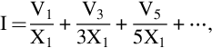
The principle of voltage control by PWM is illustrated in Fig. 2.18, which assumes a resistive load for the sake of simplicity.

There are many methods for generating PWM waveforms, but originally this was done by comparing a triangular modulating wave, the frequency of which is often referred to as “the switching frequency”, that sets the pulse frequency, shown at the top left, with a reference sinusoidal wave that determines the frequency and amplitude of the desired sinusoidal output voltage.
The inverter (on the right) is the same 3-level one discussed in Section 2.4.1, Fig. 2.14. When devices 1 and 4 are ON, the load voltage is positive and current takes the red path shown, and when devices 2 and 3 are ON the load voltage is negative and the current takes the blue path. When no devices are ON the voltage and current are both zero. With a purely resistive load, the freewheel diodes never conduct current.
The intersections of the reference and modulating wave define the switching times. Taking the positive half-cycle for example, if the amplitude of the reference wave is greater than that of the triangular wave, devices 1 and 3 are turned ON, and they remain ON until the amplitude of the reference wave becomes less than that of the triangular wave, whereupon they are turned OFF.
Readers who do not find it self-evident that this strategy generates a good waveform (i.e. one with the desired fundamental component and low harmonic content) can rest assured that it is a well-proven approach. We should also acknowledge that in a drive converter, the frequency of the modulating wave would be very much higher than that shown (for the sake of clarity) in Fig. 2.18, which in turn means that the harmonic components originating from the modulating wave will be at such a high frequency that they will be barely visible in the current waveform.
The introductory discussion above applies to a resistive load, but in the drives context the load will always include an inductive element. As a result, as we have seen earlier, when all four devices are turned OFF, the current does not fall to zero as it does with a resistive load. Instead it continues by taking the path through a pair of freewheel diodes, and within each cycle, the current will normally still be flowing until the next pair of devices turns ON, i.e. we have what we earlier called a ‘continuous current’ condition.
Typical voltage and current waveforms for an inductive load are shown in Fig. 2.19.
The output voltage no longer has any zero intervals (see Fig. 2.20 later for details), but our interest here is to show that the amplitude of the fundamental component of the output voltage is determined by the amplitude of the reference wave (dotted).

The left-hand waveform represents a medium amplitude condition in which every cycle of the modulating wave results in a switch ON and switch OFF, and in this condition the output harmonic content is modest. However when a very high amplitude is called for (on the right in Fig. 2.19), the amplitude of the reference signal may exceed that of the modulating wave for an extended period. This is the so-called ‘over-modulated’ condition, the final limit of which takes us back to the square wave, with a consequent unwelcome increase in harmonic content.
An enlarged view of the shaded region in Fig. 2.19 is shown in Fig. 2.20. This period includes the transition in the load current from the negative half-cycle (on the left of the vertical dotted line) to the positive half-cycle. The four sketches (two each on either side of the zero current crossover) represent all possible modes of operation of an inverter when there are no discontinuities in the load current. For the sake of simplicity, only the devices that are conducting are shown in each sketch.
Mode A
Ignoring the low voltage drop across each conducting device, we can see in sketch A that the load is connected to the d.c. link via the two transistors (2 and 3 in Fig. 2.18). The right-hand side of the load is connected to the positive terminal of the d.c. link, so, using the polarity convention adopted previously, the voltage across the load is negative. The current is also negative (blue), so the power is positive and energy is flowing into the load from the d.c. link.
In this particular case the load is a pure inductance, so the negative voltage causes the already negative current to increase, the additional energy being stored in the magnetic field. More generally, if the inverter is supplying a motor, this condition would correspond to motoring, with energy being supplied to the motor from the d.c. link.
Mode B
If the transistors in sketch A are switched OFF, the current that is already flowing in sketch A will have to go somewhere, because the load is inductive and the current cannot change instantaneously. Even if they were switched ON, the current cannot flow through the transistors (1 and 4 in Fig. 2.18), because they will only conduct current in one direction (down the page as we look at the diagram). The freewheel diodes shown in sketch B will therefore conduct the negative load current (blue), but because the load is now connected to the d.c. link via the two diodes, the load voltage has reversed, and is now positive.
This changeover or ‘commutation’ happens almost instantaneously: the power is now negative, and energy is flowing from the load to the d.c. link. With a pure inductive load (as here) energy is supplied from the magnetic field of the inductor, but if the inverter is supplying a motor this period would represent the recovery of excess kinetic energy from the motor and its load, an efficient technique known as ‘regenerative braking’ that we will encounter later in the book.
Mode C
If we switch transistors 1 and 4 (see Fig. 2.18) ON at any time during period B, they will not conduct until the polarity of the current becomes positive (red), whereupon the current will cease flowing in the freewheel diodes and commutate naturally to the transistors, as shown in sketch C. The load voltage and current are now both positive, so the power is positive and energy is flowing from the d.c. link to the load. The current in the load will increase.
Mode D
If we now switch OFF the transistors in sketch C the positive current must find a new path, so it flows through the freewheel diodes. The load current is positive but the voltage negative and so energy is flowing from the load to the d.c. link.
This example highlights the fact that the inverter is inherently capable of supplying or accepting energy during both positive and negative half-cycles. It will emerge later that this facility is extremely important when the inverter drives a motor.
It is also interesting, and from a design perspective important, to note that when energy is flowing from the d.c. link to the inductive load then the transistors are conducting and when energy is flowing from the load to the d.c. link the freewheel diodes are conducting. It follows that the power factor of the load therefore has a significant impact on the necessary rating of the freewheel diodes in the converter. With a low power factor load, energy flows in and out during each cycle, thereby stressing the diodes. In contrast, if the power factor is unity, there are no energy reversals, and only the transistors carry the load current.
Having digressed to look in detail at the internal modes of operation of a PWM inverter, we now return to the reason why PWM is employed, namely to control the amplitude of the output voltage wave.
It should be clear from the discussion based on Fig. 2.19 that when the frequency reaches the point at which PWM ceases to be effective in supplying the required voltage, the output waveform degenerates to a square wave whose fundamental harmonic has an amplitude of 4/π times the d.c. link voltage: the d.c. link voltage therefore determines the maximum a.c. voltage that can be produced by the inverter.
The number, width and spacing of the pulses of PWM inverters are optimised to keep the harmonic content as low as possible and fundamental voltage as high as possible. There is an obvious advantage in using a high switching frequency since there are more pulses to play with. Ultrasonic switching frequencies (generally understood to be > 16 kHz, but for we older folk switching frequencies above 10 kHz are actually inaudible!) are now widely used, and as devices improve, frequencies continue to rise. The latest Wide Band Gap devices, mentioned earlier, allow switching frequencies in the MHz range. Most manufacturers claim their particular PWM switching strategy is better than the competition, but it is not clear which, if any, is best for motor operation. Some early schemes used comparatively few pulses per cycle, and changed the number of pulses in discrete steps with output frequency rather than smoothly, which earned them the nick-name ‘gear-changers’: their sometimes irritating sound can still be heard in older traction applications. Others have irregular switching patterns, which claim to develop “white noise” rather than a single irritating tone. As a rule of thumb, the higher the switching frequency the lower the noise, but the higher the losses.
2.4.3 Three-phase inverter
Single-phase inverters are seldom used for drives, the vast majority of which use 3-phase motors because of their superior characteristics. A 3-phase output can be obtained by adding only two more switches to the four needed for a single-phase inverter, giving the typical power-circuit configuration shown in Fig. 2.21.

As usual, a freewheel diode is required in parallel with each switching device to protect against overvoltages caused by an inductive (motor) load. We note that the circuit configuration in Fig. 2.21 is essentially the same as for the 3-phase controlled rectifier discussed earlier. We mentioned then that the controlled rectifier could be used to regenerate, i.e. to convert power from d.c. to a.c., and this is, of course, ‘inversion’ as we now understand it.
This circuit forms the basis of the majority of converters for motor drives, and will be explored more fully in Chapter 7. In essence, the output voltage and frequency are controlled in much the same way as for the single-phase inverter discussed in the previous section, to produce the line-to-line output voltages (Vuv, Vvw, and Vwu) which are identical waveforms but displaced by 120° from each other. For reasons of simplicity, let us consider square wave operation, as shown in the lower part of Fig. 2.22.

The derivation of the line-line voltages can best be understood by considering the potentials of the mid-points of each leg (U, V, and W), as shown in the upper part of Fig. 2.21. The zero reference is taken as the negative terminal of the d.c. link, and the sketches show that, as expected, each mid-point is either connected to the positive terminal of the d.c. link, in which case the potential is Vdc, or to the negative (reference) in which case the potential is zero. To obtain the line voltages, for example Vuv, we subtract the potential of V from the potential of U, and this yields the three lower waveforms.
Not surprisingly, there are more constraints on switching here than in the single-phase case, because we are producing three output waveforms rather than one, and we only have two more switches to play with. In addition, it is easy to see that applying PWM to each phase may well throw up an unacceptable requirement for the upper and lower switches in one leg to be on simultaneously. Fortunately, these potential problems are limited to well-defined regions of the cycle and switching patterns or associated protection circuits include built-in delays to prevent such ‘shoot-through’ faults from occurring.
Numerous 3 phase PWM switching strategies have been developed to maximise the available voltage whilst retaining the waveform enhancing effects of PWM. The most common of these is to add third harmonic (usually 1/6 the magnitude of the fundamental) to the reference waveform. This boosts the available fundamental voltage and has no impact on torque in a symmetrically wound 3 phase a.c. motor.
It is worth mentioning at this stage that in a.c. motor drives, it is usually desirable to keep the ratio of voltage/frequency constant in order to keep the motor flux at its optimum level. This means that as the frequency of the reference sine wave is increased, its amplitude must increase in direct proportion. The frequency corresponding to the maximum available output voltage is often taken to define the ‘base speed’ of the motor, and the frequency range up to this point is often referred to as the ‘constant torque’ region, as it is only in this region that the motor is operated with its designed flux, and can therefore provide continuous rated shaft torque. Above the frequency corresponding to base speed, the inverter can no longer match voltage to frequency, the inverter effectively having run out of steam as far as voltage is concerned. The motor will then be operating at a level of flux below the design level, and the available continuous torque will reduce with frequency/speed. This region is often referred to as the ‘Constant Power’ region.
As mentioned earlier, the switching nature of these converter circuits results in waveforms which contain not only the required fundamental component but also unwanted harmonic voltages. It is particularly important to limit the magnitude of the low-order harmonics because these are most likely to provoke an unwanted torque response from the motor, but the high-order harmonics can lead to acoustic noise particularly if they happen to excite a mechanical resonance.
2.4.4 Multi-level inverter
The three-phase, three level inverter power circuit shown in Fig. 2.21, where the d.c. supply is derived from a three phase diode bridge, is widely used in drive systems rated to 2 MW and above at voltages from 400 to 690 V. At ratings above 1 MW, products designed for direct connection to medium voltage supplies (2 kV … 11 kV) are also available. At higher powers, switching the current in the devices proves more problematic in terms of the switching losses, and so switching frequencies have to be reduced. At higher voltages the impact of the rate of change of voltage on the motor insulation requires switching times to be extended deliberately, thereby further increasing losses, and limiting switching frequencies. In addition, whilst higher voltage power semiconductors are available, they tend to be relatively expensive and so commercial consideration is given to the series connection of devices. However, voltage sharing between devices then becomes a problem due to the disproportionate impact of any small difference between switching characteristics.
Multi-level converters have been developed which address these issues. One example from among many different topologies is shown in Fig. 2.23.

In this example four capacitors act as potential dividers to provide four discrete voltage levels, and each arm of the bridge has 4 series connected IGBT’s with anti-parallel diodes. The four intermediate voltage levels are connected by means of clamping diodes to the link between the series IGBT’s. To obtain full voltage between the outgoing lines all four devices in one of the upper arms are switched ON, together with all four in a different lower arm, while for say half voltage only the bottom two in an upper arm are switched ON. The quarter and three quarter levels can be selected in a similar fashion, and in this way a good ‘stepped’ approximation to a sine wave can be achieved. This can then be further enhanced by PWM.
Clearly there are more devices turned ON simultaneously than in a basic inverter, and this gives rise to an unwelcome increase in the total conduction loss. But this is offset by the fact that because the VA rating of each device is smaller than the equivalent single device, the switching loss is much reduced.
For the inverter in Fig. 2.23 the stepped waveform will have four positive, four negative and a zero level. The oscilloscope trace in Fig. 2.24 is from a 13-level inverter, and clearly displays the 13 discrete levels. A sophisticated modulation strategy is required in order not only to achieve a close approximation to a sine wave, but also to ensure that the reduction of charge (and voltage) across each d.c. link capacitor during its periods of discharge period is compensated by a subsequent charging current.

Multi-level inverters have advantages over the conventional PWM inverter:
- • A higher effective output frequency is obtained for a given PWM frequency, and smaller filter components are required.
- • EMC (Electromagnetic compatibility) is improved due to the lower dV/dt at output terminals (lower voltage steps in the same switching times), which also reduces stress on the motor insulation.
- • Higher DC link voltages are achievable for medium voltage applications due to voltage sharing of power devices within each inverter leg.
However, there are drawbacks:
- • The number of power devices is increased by at least a factor of two; each IGBT requires a floating (i.e. electrically isolated) gate drive and power supply; and additional voltage clamping diodes are required.
- • The number of DC bus capacitors may increase, but this is unlikely to be a practical problem as lower voltage capacitors in series are likely to offer a cost-effective solution.
- • The balancing of the d.c. link capacitor voltages requires careful management/control.
- • Control/modulation schemes are more complicated.
For low-voltage drives (690 V and below) the disadvantages of using a multi-level inverter tend to outweigh the advantages, with even five-level converters being significantly more expensive than conventional topologies. However multi-level converters are entering this market, so the situation may change.
2.4.5 Braking
As we have seen, the three-phase inverter power stage shown in Fig. 2.21 inherently allows power to flow in either direction between the d.c. link and the motor. However, the simple diode rectifier that is often used between the utility supply and the d.c. terminals of the inverter does not allow power to flow back into the supply. Therefore an a.c. motor drive based on this configuration cannot be used where power is required to flow from the motor to the utility supply. On the face of it, this limitation might be expected to cause a problem in almost all applications when shut down of a process is involved and the machine being driven has to be braked by the motor. The kinetic energy has to be dissipated, and during active deceleration power flows from the motor to the d.c. link, thereby causing the voltage across the d.c. link capacitor to rise to reflect the extra stored energy.
To prevent the power circuit from being damaged, d.c. link over-voltage protection is included in most industrial drive control systems. This shuts down the inverter if the d.c. link voltage exceeds a trip threshold, but this is at best a last resort. It may be possible to limit the voltage across the d.c. link capacitor by restricting the energy flow from the motor to the d.c. link by controlling the slow down ramp, but this is not always acceptable to the user.
To overcome this problem, the diode rectifier can be supplemented with a d.c. link braking resistor circuit as shown in Fig. 2.25.

In this arrangement, when the d.c. link voltage exceeds the braking threshold voltage, the switching device is turned ON. Provided the braking resistor has a low enough resistance to absorb more power than the power flowing from the inverter, the d.c. link voltage will begin to fall and the switching device will be turned OFF again. In this way the ON and OFF times are automatically set depending on the power from the inverter, and the d.c. link voltage is limited to the braking threshold. To limit the switching frequency of the braking circuit, appropriate hysteresis is included in its control. Note the freewheel diode across the braking resistor, which is required because even braking resistors have inductance!
A braking resistor circuit is used in many applications where it is practical and acceptable to dissipate stored kinetic energy in a resistor, and hence there is no longer a limit on the dynamic performance of the system.
2.4.6 Active front end
An alternative way to deal with energy flow from the inverter to the utility supply is the active rectifier shown in Fig. 2.26, in which the diode rectifier is replaced with an IGBT inverter.

The labelling of the two converters shown in Fig. 2.26 reflects their functions when the drive is operating in its normal ‘motoring’ sense, but during active braking (or even continuous generation) the converter on the left will be inverting power from the d.c. link to the utility supply, while that on the right will be rectifying the output from the induction generator.
This arrangement if often referred to as an ‘Active Front End’. Additional input inductors are usually required to limit the unwanted switching frequency currents generated by the switching action of the active rectifier, but by using PWM control the supply converter can be controlled to give near sinusoidal supply current waveforms with a power factor close to unity, so that the complete system presents a near perfect load to the utility supply.
An active rectifier is used where motoring and braking/generating operation and/or good quality input waveforms are required. Cranes and elevators, engine test rigs and cable laying ships are some applications where an active rectifier may be appropriate. The performance characteristics of this configuration are summarised below:
- • Power flow between the motor and the utility supply is possible in both directions, and so this makes the drive more efficient than when a braking resistor is used.
- • Good quality input current waveforms i.e. low harmonic distortion of the utility supply.
- • Supply power factor can be controlled to near unity (in fact it is technically possible to control this sort of bridge to operate at any power factor from approximately 0.8 lagging to 0.8 leading).
Clearly, however, an active rectifier is significantly more expensive than a simple diode rectifier and a brake resistor.
2.5 A.C. from a.c.
The converters we have looked at so far have involved a d.c. stage, but the ideal power electronic converter would allow power conversion in either direction between two systems of any voltage and frequency (including d.c.), and would not involve any intermediate stage, such as a d.c. link. In principle this can be achieved by means of an array of switches that allow any one of a set of input terminals to be connected to any one of a set of output terminals, at any desired instant. Whilst direct a.c. to a.c. converters have had only limited niche areas of application, two forms are worthy of mentioning: the Cycloconverter and the Matrix Converter.
2.5.1 The cycloconverter
The cycloconverter has always been considered a niche topology, but is still used for very large (e.g. 1 MW and above) low-speed induction motor or synchronous motor drives. The reason for its limited use lies primarily in the fact that the cycloconverter is only capable of producing acceptable output waveforms at frequencies well below the utility frequency, but this, coupled with the fact that it is feasible to make large motors with high pole-numbers (e.g. 20—see later) means that a very low-speed direct (gearless) drive becomes practicable. A 20-pole motor, for example, will have a synchronous speed of only 30 rev/min at 5 Hz, making it suitable for mine winders, kilns, crushers, etc.
The principal advantage of the cycloconverter is that naturally commutated devices (thyristors) can be used instead of self-commutating devices, which means that the cost of each device is low and high powers can be readily achieved.
The power conversion circuit for each of the three output phases is the same, so we can consider the simpler question of how to obtain a single variable-frequency supply from a three-phase supply of fixed frequency and constant voltage. We will see that in essence, the output voltage is synthesised by switching the load directly across whichever phase of the utility supply gives the best approximation to the desired load voltage at each instant of time.
Assuming that the load is an induction motor, we will discover later in the book that the power-factor varies with load but never reaches unity, i.e. that the current is never in phase with the stator voltage. So during the positive half-cycle of the voltage waveform the current will be positive for some of the time, but negative for the remainder; while during the negative voltage half-cycle the current will be negative for some of the time and positive for the rest of the time. This means that the supply to each phase has to be able to handle any combination of both positive and negative voltage and current.
We have already explored how to achieve a variable-voltage d.c. supply using a thyristor converter, which can handle positive currents, but here we need to handle negative current as well, so for each of the three motor windings we will need two converters connected in parallel, as shown in Fig. 2.27, making a total of 36 thyristors. To avoid short-circuits, between phases, isolating transformers, also shown in Fig. 2.27, are used.
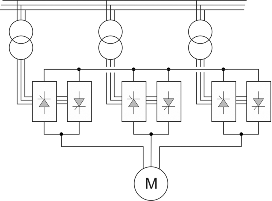
Previously the discussion focused on the mean or d.c. level of the output voltages, but here we want to provide a low-frequency (preferably sinusoidal) output voltage for an induction motor, and the means for doing this should now be becoming clear. Once we have a double thyristor converter, we can generate a low-frequency sinusoidal output voltage simply by varying the firing angle of the positive-current bridge so that its output voltage increases from zero in a sinusoidal manner with respect to time. Then, when we have completed the positive half-cycle and arrived back at zero voltage, we bring the negative bridge into play and use it to generate the negative half-cycle, and so on.
Hence the output voltage consists of chunks of the incoming supply voltage, and it offers a reasonable approximation to the fundamental-frequency sine wave shown by the dotted line in Fig. 2.28.
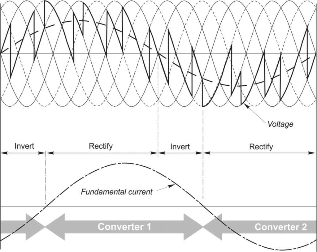
The output voltage waveform is not significantly worse than the voltage waveform from a d.c. link inverter, and as we saw in that context, the current waveform in the motor will be much smoother than the voltage, because of the filtering action of the motor self leakage inductance. The motor performance will therefore be acceptable, despite the extra losses, which arise from the unwanted harmonic components. We should note that because each phase is supplied from a double converter, the motor can regenerate when required (e.g. to restrain an overhauling load, or to return kinetic energy to the supply when the frequency is lowered to reduce speed).
2.5.2 The matrix converter
Much attention has been focused in technical journals on the matrix converter, the principle of which is shown in Fig. 2.29.
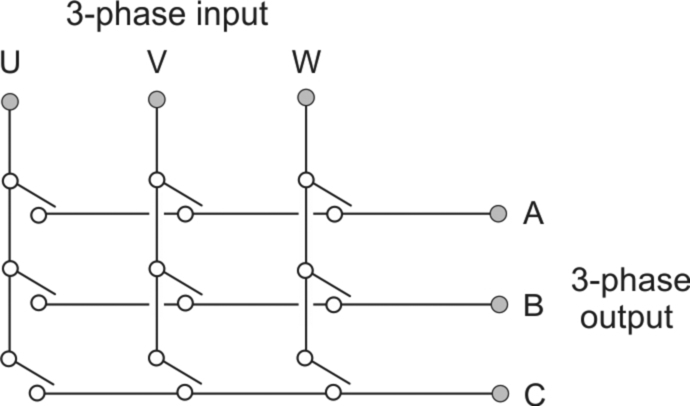
The matrix converter operates in much the same way as a cycloconverter. For example, if we assume that we wish to synthesise a 3-phase sinusoidal output of a known voltage and frequency, we know at every instant what voltage we want, say between the lines A and B, and we know what the voltages are between the three incoming lines. So we switch ON whichever pair of the A and B switches connects us to the two incoming lines whose voltage at the time is closest to the desired output line-to-line voltage, and we stay with it while ever it offers the best approximation to what we want. As soon as a different combination of switches would allow us to hook onto a more appropriate pair of input lines, the switching pattern changes.
Because there are only three different incoming line-to-line voltages to choose from, we cannot expect to synthesise a decent sinusoidal waveform with simple switching, so in order to obtain a better approximation to a sinusoidal waveform we must use chopping. This means that the switches have to be capable of switching OFF as well as ON and operating at much higher switching frequencies than the fundamental output frequency, so that switching loss becomes an important consideration.
Whilst the basic circuit is not new, recent advances in power devices offer the potential to overcome many of the drawbacks inherent in the early implementations that used discrete IGBT’s due to the lack of suitable packaged modules. On the other hand, the fact that the output voltage is limited to a maximum of 86% of the utility supply voltage (without over-modulation and subsequent loss of voltage waveform quality) means that applications in the industrial market, where standard motors predominate, remain largely problematic. However, there appear to be good prospects in some aerospace applications and possibly in some specific areas of the industrial drives market, notably integrated motors (where the drive is built into the motor, the windings of which can therefore be designed to suit the voltage available).
2.6 Inverter switching devices
As far as the user is concerned, it does not really matter what type of switching device is used inside the inverter, but it is probably helpful to mention the three most important3 families of devices in current use so that the terminology is familiar and the symbols used for each device can be recognised. The common feature of all three devices is that they can be switched ON and OFF by means of a low-power control signal, i.e. they are self-commutating. We have seen earlier that this ability to be turned ON or OFF on demand is essential in any inverter which feeds an active load, such as an induction motor.
Each device is discussed briefly below, with a broad indication of its most likely range of application. Because there is considerable overlap between competing devices, it is not possible to be dogmatic and specify which device is best, and the reader should not be surprised to find that one manufacturer may offer a 5 kW inverter which uses MOSFETs while another chooses to use IGBTs.
Power electronics is still subject to substantial innovation, and there are significant developments in the area of power semiconductor devices which are starting to impact drives. A lot of publicity and anticipation has surrounded the birth of Wide Band Gap (WBG) devices, such as Silicon Carbide and Gallium Nitride, which switch much more quickly than silicon-based devices and can operate at higher temperatures. This opens up opportunities for lower switching losses, significantly better power densities and allowing drive converters into environments which had hitherto been considered too hostile e.g. within motor windings or a jet engine. These devices therefore open up many new opportunities, but the fundamental principles of operation remain the same.
2.6.1 Bipolar junction transistor (BJT)
Historically the bipolar junction transistor was the first to be used for power switching. Of the two versions (npn and pnp) only the npn has been widely used in inverters for drives, mainly in applications ranging up to a few kW and several hundred volts.
The npn version is shown in Fig. 2.30: the main (load) current flows into the collector (C) and out of the emitter (E), as shown by the arrow on the device symbol. To switch the device ON (i.e. to make the resistance of the collector-emitter circuit low, so that load current can flow) a small current must be caused to flow from the base (B) to the emitter. When the base-emitter current is zero, the resistance of the collector-emitter circuit is very high, and the device is switched OFF.

The advantage of the bipolar transistor is that when it is turned ON, the collector-emitter voltage is low (see point b in Fig. 2.3) and hence the power dissipation is small in comparison with the load power, i.e. the device is an efficient power switch. The disadvantage is that although the power required in the base-emitter circuit is tiny in comparison with the load power, it is not insignificant and in the largest power transistors can amount to several tens of watts.
2.6.2 Metal oxide semiconductor field effect transistor (MOSFET)
Since the 1980s the power MOSFET has superseded the BJT in inverters for drives. Like the BJT, the MOSFET is a three-terminal device and is available in two versions, the n-channel and the p-channel. The n-channel is the most widely used, and is shown in Fig. 2.30. The main (load) current flows into the drain (D) and out of the source (S). (Confusingly, the load current in this case flows in the opposite direction to the arrow on the symbol.) Unlike the BJT, which is controlled by the base current, the MOSFET is controlled by the gate-source voltage.
To turn the device ON, the gate-source voltage must be comfortably above a threshold of a few volts. When the voltage is first applied to the gate, currents flow in the parasitic gate-source and gate-drain capacitances, but once these capacitances have been charged the input current to the gate is negligible, so the steady-state gate drive power is minimal. To turn the device OFF, the parasitic capacitances must be discharged and the gate-source voltage must be held below the threshold level.
The principal advantage of the MOSFET is that it is a voltage-controlled device which requires negligible power to hold it in the ON state. The gate drive circuitry is thus less complex and costly than the base drive circuitry of an equivalent bipolar device. The disadvantage of the MOSFET is that in the ON state the effective resistance of the drain-source is higher than an equivalent bipolar device, so the power dissipation is higher and the device is rather less efficient as a power switch. MOSFETs are used in low and medium power inverters up to a few kW, with voltages generally not exceeding 700 V.
2.6.3 Insulated gate bipolar transistor (IGBT)
The IGBT (Fig. 2.30) is a hybrid device which combines the best features of the MOSFET (i.e. ease of gate turn ON and turn OFF from low-power logic circuits) and the BJT (relatively low power dissipation in the main collector-emitter circuit). These obvious advantages give the IGBT the edge over the MOSFET and BJT, and account for their dominance in all but small drives. They are particularly well suited to the medium power, medium voltage range (up to several hundred kW). The path for the main (load) current is from collector to emitter, as in the npn bipolar device.
2.7 Converter waveforms, acoustic noise, and cooling
In common with most textbooks, the waveforms shown in this chapter (and later in the book) are what we would hope to see under ideal conditions. It makes sense to concentrate on these ideal waveforms from the point of view of gaining a basic understanding, but we ought to be warned that what we see on an oscilloscope may well look rather different, and is often not easy to interpret.
We have seen that the essence of power electronics is the switching process, so it should not come as much of a surprise to learn that in practice the switching is seldom achieved in such a clear-cut fashion as we have assumed. Usually, there will be some sort of high-frequency oscillation or ‘ringing’ evident, particularly on the voltage waveforms following each transition due to switching. This is due to the effects of stray capacitance and inductance: it will have been anticipated at the design stage, and steps will have been taken to minimise it by fitting ‘snubbing’ circuits at the appropriate places in the converter. However complete suppression of all these transient phenomena is seldom economically worthwhile so the user should not be too alarmed to see remnants of the transient phenomena in the output waveforms.
Acoustic noise is also a matter that can worry newcomers. Most power electronic converters emit whining or humming sounds at frequencies corresponding to the fundamental and harmonics of the switching frequency, though when the converter is used to feed a motor, the sound from the motor is usually a good deal louder than the sound from the converter itself. These sounds are difficult to describe in words, but typically range from a high-pitched hum through a whine to a piercing whistle. In a.c. drives it is often possible to vary the switching frequency, which may allow specific mechanical resonances to be avoided. If taken above the audible range (which is inversely proportional to age) the sound clearly disappears, but at the expense of increased switching losses, so a compromise has to be sought.
2.7.1 Cooling of switching devices—Thermal resistance
We have seen that by adopting a switching strategy the power loss in the switching devices is small in comparison with the power throughput, so the converter has a high efficiency. Nevertheless almost all the heat which is produced in the switching devices is released in the active region of the semiconductor, which is itself very small and will overheat and breakdown unless it is adequately cooled. It is therefore essential to ensure that even under the most onerous operating conditions, the temperature of the active switching junction inside the device does not exceed the safe value.
Consider what happens to the temperature of the junction region of the device when we start from cold (i.e. ambient) temperature and operate the device so that its average power dissipation remains constant. At first, the junction temperature begins to rise, so some of the heat generated is conducted to the metal case, which stores some heat as its temperature rises. Heat then flows into the heatsink (if fitted) which begins to warm up, and heat begins to flow to the surrounding air, at ambient temperature. The temperatures of the junction, case and heatsink continue to rise until eventually an equilibrium is reached when the total rate of loss of heat to ambient temperature is equal to the power dissipation inside the device.
The final steady-state junction temperature thus depends on how difficult it is for the heat to escape down the temperature gradient to ambient, or in other words on the total ‘thermal resistance’ between the junction inside the device and the surrounding medium (usually air). Thermal resistance is usually expressed in °C/W, which directly indicates how much temperature rise will occur in the steady state for every Watt of dissipated power. It follows that for a given power dissipation, the higher the thermal resistance, the higher the temperature rise, so in order to minimise the temperature rise of the device, the total thermal resistance between it and the surrounding air must be made as small as possible.
The device designer aims to minimise the thermal resistance between the semiconductor junction and the case of the device, and provides a large and flat metal mounting surface to minimise the thermal resistance between the case and the heatsink. The converter designer must ensure good thermal contact between the device and the heatsink, usually by a bolted joint smeared with heat-conducting compound to fill any microscopic voids, and must design the heatsink to minimise the thermal resistance to air. Heatsink design offers the only real scope for appreciably reducing the total resistance, and involves careful selection of the material, size, shape and orientation of the heatsink, and the associated air-moving system (see below).
In some applications, air cooled heatsinks are not the best choice, and alternatives such as liquid cooling (de-ionised water, glycol or oil) is used. An automotive application is a typical example of this, where a drive can be designed to take advantage of an existing liquid cooling system.
One drawback of the good thermal path between the semiconductor junction and the case of the device is that the metal mounting surface (or surfaces in the case of the popular high power hockey-puck package) can be electrically ‘live’. This poses a difficulty for the converter designer, because mounting the device directly on the heatsink causes the latter to be potentially dangerous. In addition, several separate isolated heatsinks may be required in order to avoid short-circuits. The alternative is for the devices to be electrically isolated from the heatsink using thin mica spacers, but then the thermal resistance is increased appreciably.
Increasingly devices come in packaged ‘modules’ with an electrically isolated metal interface to get round the ‘live’ problem. The packages contain combinations of transistors, diodes or thyristors, from which various converter circuits can be built up. Several modules can be mounted on a single heatsink, which does not have to be isolated from the enclosure or cabinet. They are available in ratings suitable for converters up to hundreds of kW, and the range is expanding.
2.7.2 Arrangement of heatsinks and forced-air cooling
The principal factors which govern the thermal resistance of a heatsink are the total surface area, the condition of the surface and the air flow. Many converters use extruded aluminium heatsinks, with multiple fins to increase the effective cooling surface area and lower the resistance, and with a machined face or faces for mounting the devices. Heatsinks are usually mounted vertically to improve natural air convection. Surface finish is important, with black anodised aluminium being typically 30% better than bright. The cooling performance of heatsinks is however a complex technical area, with turbulence being very beneficial in forced air-cooled heatsinks.
A typical layout for a medium-power (say 200 kW) converter is shown in Fig. 2.31. The fan(s) are positioned either at the top or bottom of the heatsink, and draw external air upwards, assisting natural convection. Even a modest airflow is very beneficial: with an air velocity of only 2 m/s, for example, the thermal resistance is halved as compared with the naturally-cooled set-up, which means that for a given temperature rise the heatsink can be half the size of the naturally-cooled one. However, large increases in the air velocity bring diminishing returns and also introduce additional noise.

2.8 Review questions
- (1) In the circuit of Fig. Q1 both voltage sources and the diodes can be treated as ideal, and the load is a resistor. (Note: this question is specifically aimed at reinforcing the understanding of how diodes behave: it is not representative of any practical circuit.)
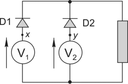
Fig. Q1
Sketch the voltage across the load under the following conditions:- (a) V1 is a sinusoid of amplitude 20 V, and V2 is a constant voltage of + 10 V;
- (b) V1 is a sinusoid of amplitude 20 V, and V2 is a constant voltage of − 10 V;
- (c) The same as (a), except that the diode D1 is placed below, rather above, V1.
- (2) What is the maximum d.c. voltage available from a fully-controlled bridge converter supplying a motor and operating from a low-impedance 230 V utility supply?
- (3) Estimate the firing angle required to produce a mean output voltage of 300 V from a fully-controlled three-phase converter supplied from stiff 415 V, 50 Hz utility supply. Assume that the load current is continuous. How would the firing angle have to change if the supply frequency was 60 Hz rather than 50 Hz?
- (4) Sketch the waveform of voltage across one of the thyristors in a fully-controlled single-phase converter with a firing angle delay of 60°. Assume that the d.c. load current is continuous. Fig. 2.10 may prove helpful.
- (5) Sketch the current waveform in the a.c. supply when a single-phase fully-controlled converter with α = 45° is supplying a highly inductive load which draws a smooth current of 25 A. If the a.c. supply is 240 V, 50 Hz, and losses in the devices are neglected, calculate the peak and average supply power per cycle.
- (6) A d.c. chopper circuit is often said to be like an a.c. transformer. Explain what this means by considering the input and output power relationships for a chopper-fed inductive motor load supplied with an average voltage of 20 V from a 100 V battery. Assume that the motor current remains constant throughout at 10 A.
- (7) A 5 kHz step-down transistor chopper operating from a 150 V battery supplies an R/L load which draws an almost-constant current of 5 A. The resistance of the load is 8 Ω.
Treating all devices as ideal, estimate:- (i) the mark:space ratio of the chopper;
- (ii) the average power in the load;
- (iii) the average power from the source.
- (8) This question relates to the switching circuit of Fig. Q8, and in particular to the function of the diode.
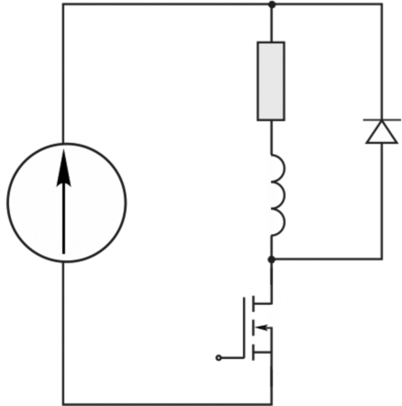
Fig. Q8
Some possible answers to the question ‘what is the purpose of the diode’ are given below:- • to prevent reverse current in the switch
- • to protect the inductor from high voltages
- • to limit the rate of change of current in the supply
- • to limit the voltage across the MOSFET
- • to dissipate the stored energy in the inductance
Discuss these answers and identify which one(s) are correct. - (9) In the circuit of Fig. Q8, assume that the supply voltage is 100 V, and that the forward volt-drop across the diode is 0.7 V. Some common answers to the question ‘when the current is freewheeling, what is the voltage across the MOSFET’ are given below:
- • 99.3 V
- • 0.7 V
- • zero
- • depends on the inductance
- • 100.7 V
Discuss these answers and identify which one is correct.
Answers to the review questions are given in the Appendix.