
Amplifiers
Abstract
Amplifiers turn a small signal into a larger, more powerful version of the same. Mastering amplification is useful in itself as well as an important exercise in circuit design. Amplifier characteristics include gain, noise, and bandwidth. This chapter concentrates on the design of MOSFET amplifiers. The basic characteristics of op amps are introduced and op amp topologies useful for amplification are described. Design examples include a two-stage amplifier for a low-impedance load and an op amp electret microphone amplifier.
Keywords
Amplifiers; MOSFET amplifiers; Op amps; Gain; Noise
4.1 Introduction
Amplifiers represent the simplest transformation we make on signals—we turn a small signal into a larger, more powerful version of the same. But this simple task involves many subtleties. Mastering amplification is useful in itself as well as an important exercise in circuit design.
Designing amplifiers requires us to understand transistors in more detail. Discrete transistors can be used to build a wide range of amplifiers. Fig. 4.1 shows two types of packages: TO-220 on the left and TO-92 on the right. We will also study integrated amplifiers in the form of op amps.

The next section introduces the basic specifications for amplifiers. Section 4.3 discusses analysis methods for circuits. Section 4.4 develops circuit models for the MOSFET. Section 4.5 introduces amplifier topologies. Section 4.6 designs an amplifier for a low-impedance load. Section 4.7 briefly introduces concepts in power amplifiers. Section 4.8 considers integrated amplifiers as useful components. Section 4.9 introduces the op amp, a versatile component. Section 4.10 considers noise, interference, and crosstalk. Section 4.11 looks at the design of an amplifier for a microphone.
4.2 Amplifier Specifications
We use amplifiers because they provide gain, represented by the variable A. We can talk about power, voltage, or current gain, depending on how we prefer to think about the signals. The most common form used in amplifier design is voltage gain:

A negative value for gain means that the output is 180 degrees out of phase with the input: when the input is high, the output is low; when the input is low, the output is high. Many amplifier topologies naturally produce inverted outputs and are characterized by negative gain.
We are particularly concerned with the load impedance that the amplifier is able to drive. The input characteristics of the amplifier are also of interest.
Since neither the devices nor circuits that make up the amplifier are ideal, we are also interested in specifying the tolerable level of variations from the ideal. When we compare the output of an amplifier to a known input, such as a sinusoid, we measure its distortion. Some forms of distortion are linear; they generate harmonic distortion. When we inject a sinusoidal signal PF at the fundamental frequency into the amplifier's input, harmonic distortion appears as a set of harmonic signals PH, i. We can define total harmonic distortion (THD) as

Nonharmonic distortions are known as intermodulation distortion (IM). When we inject two sinusoids that are not harmonically related into the amplifier's input, intermodulation generates signals at other frequencies. If the input signals are at frequencies f1, f2, f2 > f1, the intermodulation products include sums and products of multiples of the input frequencies:
The order of the harmonic is given by m + n. Intermodulation products that are near the frequency of interest are of particular concern. We generally measure the different intermodulation products individually and measure the ratio of the RMS intermodulation voltage to the fundamental RMS voltage.
Another important form of nonideality is noise. We specify amplifiers based on signal-to-noise ratio (SNR), or the ratio between the largest signal the amplifier can produce to the noise it produces; we also refer to this ratio as dynamic range. These values are often cited in decibels. We will discuss noise, interference, and crosstalk in Section 4.10.
4.3 Circuit Analysis Methods
Transistors are nonlinear, active elements that we can use to build linear circuits. Amplifiers are very useful in themselves; amplifier design also allows us to learn and practice a wide range of circuit analysis and design techniques.
Circuit designers often refer to DC and AC analysis. Since we can break down any signal into the sum of a constant value and a changing value, we can use this decomposition to help us understand circuits. DC analysis assumes no signals in the circuit change. We often want to place some terminals of a transistor at a given voltage known as a bias voltage. The device may require that some terminals are kept at a prescribed voltage: bipolar transistors require a voltage across their base-emitter junction to turn on the transistor; MOSFETs require their gate voltage to be above the threshold voltage. We may also want to put some terminals at a given voltage to ensure that signals, when they do change, can swing through their full range. DC analysis allows us to determine bias voltages and the operating point of the transistor. AC analysis can separately consider the effects of changing signals. We traditionally use capital letters for DC variables (I1, V1) and lowercase letters for AC variables (i2, v2).
Circuit designers also refer to small-signal and large-signal analysis. While transistors are nonlinear devices, we can approximate them with linear models over some of their operating range and under the assumption that signals are small. A small-signal model provides an equivalent circuit for a transistor under conditions that allow the transistor to be treated as a linear component. Under small-signal analysis, we replace the device with its small-signal model; we also replace DC voltage sources with short circuits and DC current sources with open circuits. We typically use small letters such as i1, v1 for small-signal values. However, small-signal assumptions do not hold in some circuits, with power amplifiers being a classic example. We use large-signal models in these cases. Typically, we use graphical methods to solve for the behavior of the transistor under large-signal assumptions: starting with the set of operating curves for the transistor, we draw additional lines that represent the constraints imposed on the transistor operation by other circuit components.
We will take advantage of schematic capture and simulation tools in this chapter. Circuit simulators, as described in Section 1.9, allow us to solve for the waveforms of complex circuits with nonlinear elements; they also provide other forms of analysis such as noise. Free versions of CAD tools are limited in capability relative to paid tools but still provide valuable capabilities.
4.4 MOSFET Transistor Models
We can model the MOSFET using both small-signal and large-signal models. For each model, we need to determine the model parameters from the given parameters of the particular transistor we want to use. Data sheets may or may not directly give us the required parameters; in such cases we need to derive the model parameters from the given values.
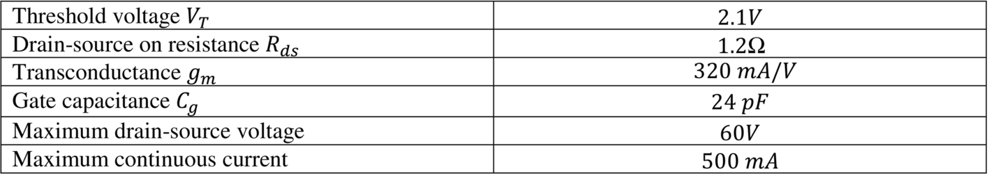
We will use as an example the Fairchild BS170 n-type MOSFET [18]. Fig. 4.2 gives some of this transistor's parameters.
4.4.1 Small-Signal Models
Figs. 4.3 and 4.4 show two small-signal models for a MOSFET: the pi model takes the form of the Greek letter; the t model uses a T-shaped circuit topology. These two models are equivalent; in any given situation, one may be more convenient than the other. The diamond-shaped current source represents a controlled source—the current depends on another circuit variable.

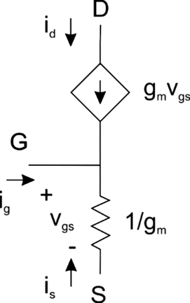
The transistor's transconductance gm relates input voltage to output current. The MOSFET gate's high capacitance gives an open circuit in this model. The resistance r0 models the resistance between the drain and source. In the t model form, the gate current is always zero.
4.4.2 Large-Signal Models
As we saw in Section 3.3, a MOSFET has a linear region corresponding to low drain-source voltages and a saturation region corresponding to high VDS. It also has a cutoff region when the gate voltage is below the device's threshold voltage, but that is not directly represented in the characteristic curves.
The large-signal model [57] reflects these three modes of operation. Fig. 4.5 shows a simple large-signal model for a MOSFET's saturation mode. The voltage across the gate capacitance controls the drain-source current source.

Vt is the threshold voltage below which the MOSFET drain-source region does not conduct. k′ is a parameter that depends on device physics. W/L gives the width/length ratio of the MOSFET channel, which scales the magnitude of the current; this parameter is of more interest to integrated circuit designers who can choose the sizes of their transistors. When using discrete MOSFETs we are generally given the drain current for a given gate voltage.
To properly simulate this transistor in PSpice, we need to set the MOSFET model parameter using the Model Editor shown in Fig. 4.6. The PSpice model was designed for integrated circuit design in which we know the width and length of the transistor channel. In this case, we set the transistor width and length to 1. We estimate ![]() .
.

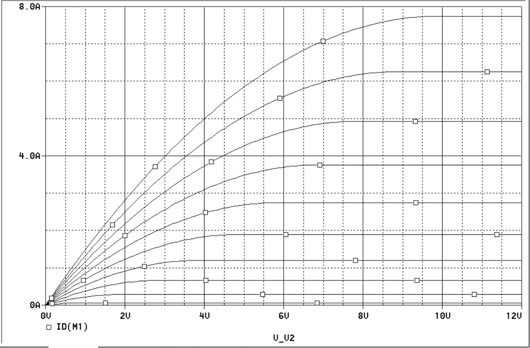
We can trace the characteristic curves of a MOSFET. Fig. 4.7 shows the setup. In this case, the gate is driven by a voltage source. We sweep both the drain-source voltage and the gate voltage. The results are shown in Fig. 4.8. These curves clearly show the linear and saturation regions of the transistor's operation.

4.5 MOSFET Amplifier Topologies
We can incorporate the MOSFET into amplifiers with several different topologies. Each has its own advantages and disadvantages.
4.5.1 Common Source Amplifier
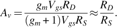
Fig. 4.9 shows a common source amplifier. This topology provides good voltage gain. The high gate impedance of the MOSFET gives this topology a high input impedance.
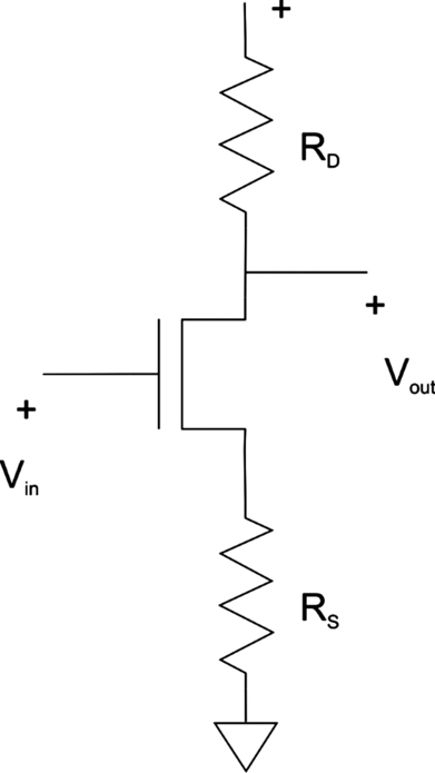
We can analyze the voltage gain of the common source amplifier using AC analysis and the MOSFET small-signal model of Fig. 4.10. The input source and power supply become shorts in AC analysis. The model circuit is shown in Fig. 4.10. If r0 ≫ RD, the output voltage is Vds = gmVgsRD; the input voltage is Vgs = (gm + 1)VgsRS. When we substitute these terms into the definition of voltage gain, we find

Large-signal analysis starts with a load line for the circuit—the load line describes the drain-source current over a range of drain-source voltages. Fig. 4.11 shows that in this case the load line is defined by VDD on one end and VDD/RL at the other end. We select a quiescent point or Q point that represents VDS when the input is zero; the Q point is typically put at the middle of the operating region of the load line.

4.5.2 Common Drain Amplifier
Fig. 4.12 shows the common drain or source follower configuration. This topology provides unity voltage gain and a relatively high output impedance that makes it useful for driving low-impedance loads. Once again, the MOSFET's gate impedance ensures high input impedance.

4.5.3 Common Gate Amplifier
Fig. 4.13 shows the common gate configuration. This configuration provides unity current gain and good voltage gain. Because the gate is not at the input, it has low input impedance. It provides a high output impedance making it useful for driving low-impedance loads.
4.5.4 Cascode Amplifier
We can also design a cascode amplifier using MOSFETs as shown in Fig. 4.14. M1 is configured as a common emitter while M2 is used as an emitter follower. The signal input is provided to the gate of M2.

4.5.5 Differential Amplifier
Fig. 4.15 shows the differential amplifier. This topology is widely used to compare two signals and amplify the difference between them. The currents of the two legs defined by M1, M2 are related to each other through the current source—the sum of the currents through the two legs is constant. Differences in the input voltages V+, V− result in amplified differences in the output voltages V1, V2.

4.5.6 Current Sources
The differential amplifier makes use of a current source as do many other circuits. An ideal current source produces a known current independent of load. We can build realistic current sources with various degrees of fidelity to that goal, each with its own advantages and disadvantages.
Fig. 4.16 shows a basic current source circuit. The voltage divider provides a gate voltage for the MOSFET that governs its drain-source current. This circuit is adequate for simple applications but is prone to several problems: variations in the power supply voltage will cause variations in the output current; temperature variations will cause the transistor gain to change, resulting in a change in the output current; inaccuracies in the resistor values will cause an unanticipated output current.

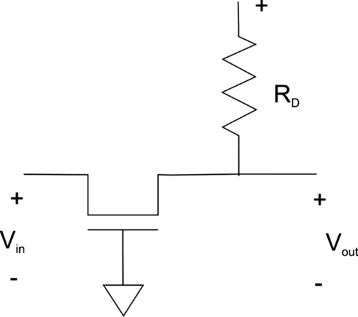
A current mirror is used to copy an input current to an output current while isolating the input from the output. Current mirrors are designed with low input impedance to minimize input voltage variations; they provide high output impedance to reduce variations caused by the load. Several current mirror circuits have been designed; one example is the Widlar current mirror of Fig. 4.17. Accurate current mirrors require matched transistors so building one out of discrete transistors may be counterproductive. Several integrated circuit current mirrors are available that take advantage of the good matching characteristics of ICs.
4.6 Example: Driving a Low-Impedance Load
We can use the basic amplifier circuits to build a two-stage amplifier designed to drive a low-impedance load using MOSFETs. Given a circuit topology for the amplifier, we can derive several models for different analytical purposes. For each stage, we establish some large-signal parameters and then use those values to determine the component values.
This example gives us the chance to consider some practicalities. While we may calculate particular values for our components, we can’t procure components with those exact values. Resistors, inductors, and capacitors all come in standard values. Those values are chosen to provide a good range of values and avoid gaps in coverage. Nonetheless, we must make use of the available values, which is one reason to design robust circuits that are tolerant of variations.
Beyond choosing fixed values, we must take into account the fact that passive components are manufactured to certain tolerances. For example, a 47 kΩ resistor with a tolerance of ± 10% could have an actual value ranging from 42.3 to 5.17 kΩ. Components are generally available in several different tolerances; tighter tolerances cost more money. Matching of component values is particularly important for symmetric circuits. For example, the difference in value of the two resistors on the legs of a differential amplifier has a greater effect on the performance of the amplifier than does their absolute values, at least within reasonable tolerances. Unmatched resistors in the two legs of the differential pair lead to different voltages and currents in the legs even when the input voltages are identical.
Passive components are also given maximum power ratings. A component should not be operated at a power level higher than its rating. In general, some amount of headroom should be left in the power rating. Given the variation of component values and other operating conditions, devices operating at close to their rated power level may occasionally exceed that level, causing reliability problems.
4.6.1 Amplifier Specifications and Topology
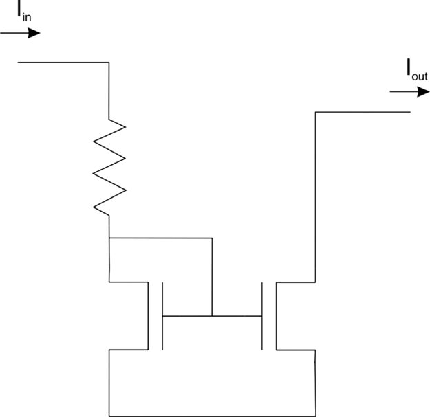
Fig. 4.18 shows the OrCAD schematic for the amplifier, which is organized into two stages. The first stage uses M1 in a common-source configuration; the second stage uses M2 as a source follower/common-drain.
The amplifier is designed around a 12 V power supply. Our specifications include a voltage gain Av = − 10 and the ability to drive an 8 Ω load, which is the typical impedance for a large speaker (smaller speakers generally have a 4 Ω impedance). The amplifier should work over the standard audio range of [fL, fH] = [100 Hz, 20 kHz]. We assume that the impedance of the source is 1 kΩ. We can choose the component values starting at the input and, for the most part, move through to the output. We will simulate the circuit using the transistor model we used in Section 4.4.1.
4.6.2 Input and First Stage
We will use the BS170 MOSFET for both stages [18]; it has a maximum voltage of 60 V and gm = 320 mS, k′ = 17 mS, VT = 2.1 V, ID,SAT = 0.5 A.
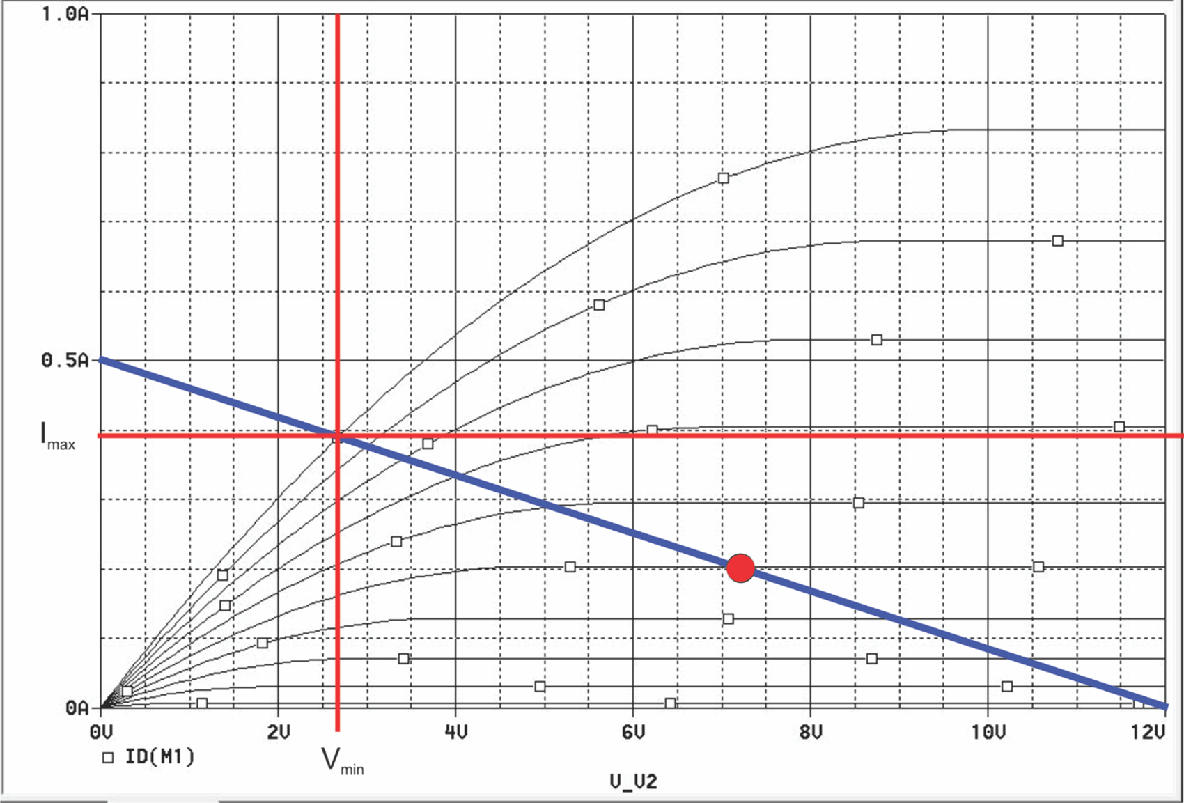
The first stage will supply all of the voltage gain for the amplifier. Given that we use the second stage for current amplification, we have some freedom in how we choose the maximum drain current, so we choose a value of Imax = 0.4 A which occurs at Vmin = 2.3 V. Fig. 4.19 shows the load line based on the transistor curves, the power supply voltage, and the chosen drain current. We choose VQ = 7.25 V as an quiescent point, the midpoint of the operating region of the load line.
We use the voltage gain and collector current to determine the values for RD and RS1. Within the desired frequency response of the amplifier, RS1 is shorted out by CS1. We can determine the value for RD by substituting the small-signal MOSFET model into a small-signal model of the amplifier. As shown in Fig. 4.20, the power supply appears as a short in the small-signal model, so RD is connected in parallel with the MOSFET's internal resistance ro. Since RD ≫ ro, we can approximate the gain as


Substituting our values for Av and gm, we find that RF = 33 Ω.
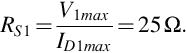
We choose RS1 to provide a reasonable voltage between the MOSFET's source and ground, one large enough to allow for the maximum output swing of the first stage. If we allow a maximum swing of V1max = 5 V at a current of ID1max = 0.2 A, then
The resistors R1 and R2 are the bias network for M1. They form a voltage divider to set the gate voltage for M1: their ratio determines the bias voltage while their sum determines the current running through the bias circuit. We have chosen a bias voltage for the gate of 6 V. Given the MOSFET's high impedance, we have a great deal of freedom in choosing the bias resistor values. A good approach is to choose large values that result in a small current in the bias network. We choose R1 = R2 = 1 MΩ.
We also need to find a value for the source bypass capacitor CS1. The parallel combination of RS1, CS1 should appear as a short within the operating frequency range of the amplifier. We achieve this by setting the − 3 dB point of CS, RS should be at fL = 100 Hz. We know from Section 1.4 that the − 3 dB point occurs at half power or ![]() voltage. This condition occurs when the resistance equals the capacitive reactance:
voltage. This condition occurs when the resistance equals the capacitive reactance:

We also need to find a value for the input coupling capacitor CS. This capacitor DC-decouples the input from the transistor's bias network. We substitute into Eq. (4.10) to find that CS = 63 μF which we round to CS = 66 μF.
Fig. 4.21 shows the output of the first stage. The measured gain is approximately 5, lower than the target value for the gain. The initial drift in voltage is due to the charging of the capacitors.

4.6.3 Second Stage and Output
The second stage does not need a bias network because the first stage output maintains a reasonable operating voltage for M2. This stage uses a common drain topology, also known as a source follower, to provide strong drive to the low-impedance output without increasing voltage gain. This topology means that there is no drain resistor.
We choose the source resistance RS2 to ensure that the worst-case voltage swing does not push the MOSFET's source voltage to the negative power supply:
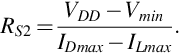
We choose a minimum source voltage of Vmin = 3 V and a maximum drain current of IDmax = 0.5 A. If we allow a maximum current to the load of ILmax = 0.05 A, then we find RS2 = 20 Ω which we approximate as RS2 = 25 Ω.
We set the value of C2 to provide an appropriate rolloff frequency given the load resistance of 8 Ω, giving us C2 = 199 μF which we approximate as C2 = 188 μF.
Fig. 4.22 shows output waveform for the amplifier's second stage as measured across RL.

4.7 Power Amplifiers
The amplifier techniques from Section 4.6 are not always suited to the design of large power amplifiers. We do not often need to build our own power amplifiers for computer interfaces but a brief discussion helps to highlight some interesting aspects of amplifier design.
Linear amplifiers generate higher-powered output signals that follow their lower-powered inputs. By biasing the amplifier in different ways, we can create different classes of amplifier with different characteristics.
A Class A amplifier is biased to the middle of its operating range, allowing symmetric input signal swings. The amplifiers of Section 4.small-signal-amp were designed for Class A operation. Class A amplifiers offer the least distortion but also the highest power consumption. When the input voltage is zero, the Class A amplifier produces a large output current and consuming power.
A Class B amplifier is biased so that it operates for only half of the waveform. Since we often want to amplify both sides of the input waveform, we can connect two Class B drivers in a push-pull configuration. One driver pulls up for positive outputs while the other driver pulls down for negative outputs. The Class B amplifier stages do not produce output currents when the input voltage is zero. The tradeoff for lower power consumption is somewhat higher distortion. We can build Class AB amplifiers by biasing the drivers so that each operates for more than half of the input cycle, somewhat reducing distortion.
A Class C amplifier amplifies for less than half of the input cycle.
Class D amplifiers are not linear. The D does not stand for digital, however. These amplifiers use pulse width modulation to modulate the power supplied to the output [29]. An output filter transforms the pulse-modulated train into the desired continuous signal. Class D amplifiers are extremely power efficient; they can be operated without heat sinks up to a surprisingly high output power level. Class D amplifiers for speakers, which present inductive loads, share some design issues with motor controllers; we will discuss motor controllers in more detail in Section 8.13.
Thermal dissipation is an important design consideration for power amplifiers. Most of the electrical energy put into the circuit comes out as heat. If the components become too hot, they will degrade and eventually fail. While all components are subject to heat problems, transistors are most critical to protect. When the interior of the transistor reaches the maximum junction temperature Tj = 85°C, the semiconductor junctions of the device are damaged. We use heat sinks to help dissipate the heat energy generated by transistors.
We can calculate the junction temperature using a steady-state model. Each component has a thermal resistance which describes the flow of heat. The transistor data sheet provides a thermal resistance from junction to case; in the case of our example transistor, RθJC = 83.3°C/W [20]. The heat sink has its own thermal resistance RθHS. For our simple model, we can consider these two thermal resistances to be in series, much as electrical resistances. Power dissipation in the heat equation is analogous to current in electrical circuits. The amplifier operates in an environment at an ambient temperature; the environment is analogous to ground in an electrical circuit. We can find the junction temperature as the increase in temperature above the ambient given the thermal resistance and power consumption:
4.8 Integrated Amplifiers
As much fun as it is to design and build your own transistor amplifiers, using an integrated amplifier often makes more sense. Integrated circuits provide much better matching of components and lower parasitic values, improving amplifier performance. Integrated amplifiers are also physically small.
The TPA6138A2 [64] is designed to drive headphones, providing 40 mW into 32 Ω. External resistors are used to set the amplifier gain. It includes circuitry to reduce clicks and pops caused by plugging and unplugging the headphones.
The LM380 [40] is a 2.5 W power amplifier for audio. It provides a fixed gain of 50 (34 dB) to reduce the cost of the circuit; volume control can be provided by preamplifier stages feeding the LM380.
The TPA6404-Q1 [69] is designed for automotive audio systems. At its core is a 50 W class D amplifier. It provides control and diagnostics using the I2C bus. Some amplifiers provide digital input. The TAS6424L-Q1 [68], for example, provides I2C input of the audio channels as well as control and diagnostics.
The WM9801 [13] combines a DAC with an amplifier. The chip provides both class AB and class D amplifier modes. Digital logic is used for filtering, volume control, parametric equalization, and dynamic range control.
The LM386 [70] is a widely used low-voltage audio power amplifier. It can operate on power supply voltages in the range 4–12 V with gains in the range 20–200. Its low power supply voltage and reasonable gain make it popular in small guitar amplifiers and portable consumer audio equipment.
4.9 Op Amps
Integrated audio amplifiers are designed for particular applications. The operational amplifier or op amp, in contrast, is designed as a general-purpose component used to build specific circuits. Op amps are used in all sorts of ways in circuit design. We will cover more sophisticated uses of op amps in more detail in Chapter 5; here we concentrate on their use as amplifiers.
The schematic symbol for an op amp is shown in Fig. 4.23. It has two inputs, + and −. The one output value is formed by the difference of the two inputs. An op amp requires a power source but we will typically omit their power connections in our illustrations. The 741 is a classic op amp but other designs provide a range of operating characteristics.

An ideal op amp has three basic characteristics:
- • Infinite input impedance.
- • Infinite gain.
- • Zero output impedance.
Real op amps cannot provide these superlative characteristics but reasonable circuits can provide very good approximations of them over a wide range of frequencies. A typical op amp circuit is built from two major blocks: a differential amplifier compares the two input voltages; a voltage amplifier is used to provide voltage gain for the differential amplifier's result. Op amps are mainstays for small-signal amplification. While op amps generally do not provide the drive capability required for large power amplifiers, they can be used as an input stage. Many power amplifiers also use differential input stages similar to those used in op amps.
An op amp without feedback will produce output voltages at one extreme or the other based on the polarity of V+ − V−. We generally use feedback circuits to control the op amp.
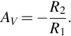
Fig. 4.24 shows a linear amplifier built from an op amp [41]. This is an inverting amplifier with voltage gain
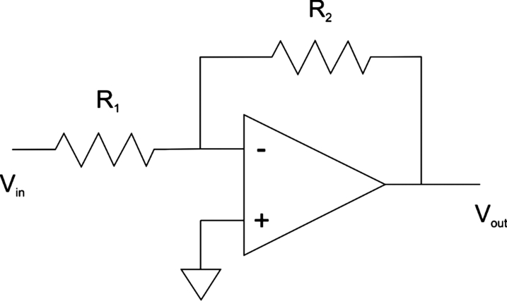
For example, R2 = 10 kΩ, R1 = 1 kΩ gives AV = 10. This formula is easy to derive. Since the input terminals have infinite impedance, no current flows into them so:
We can rearrange the terms and obtain the gain formula of Eq. (4.13).
Fig. 4.25 shows a noninverting topology for an amplifier. The gain in this case is
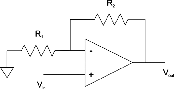
In the noninverting case, R2 = 10 kΩ, R1 = 1 kΩ gives AV = 11.
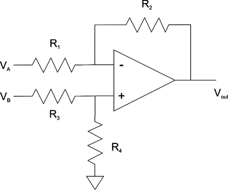
Fig. 4.26 shows an op amp used to generate the difference between the two inputs. When all four resistors have the same value, the output is VB − VA. We can generate weighted differences by changing the relative values of the resistors.
Real op amps have nonideal characteristics that will affect circuit design to some degree [32]. The most important is its finite bandwidth. We evaluate bandwidth using open loop gain. While an op amp has a very high (albeit finite) gain, that gain starts to roll off quickly: the − 3 dB point of the μA741 op amp is about 5 Hz [60]; other op amps may roll off at hundreds of hertz. The gain rolls off at 6 dB per decade. The unity gain point is the frequency at which the op amp's gain is 1. The μA741, for example, has a unity gain frequency of about 1 MHz. When we use the op amp in a closed-loop circuit, we want to be sure that the closed loop gain at the maximum required frequency is considerably larger than the op amp's open loop gain at that frequency. A good rule of thumb is that the op amp should have an open loop bandwidth of at least 10X the required closed-loop bandwidth [32].
Slew rate describes the large-signal behavior of the op amp; slew rate is also used to evaluate other types of amplifiers. Slew rate is defined as the ratio of change in output voltage per unit time:

Slew rate is limited by the amplifier's maximum output current. The μA741 has a slew rate at unity gain of 0.5 V/μs.
The noise of an op amp will limit the dynamic range through which it can be operated.
Common mode rejection ratio (CMRR) measures the response of the op amp to the same voltage on both its input terminals. The magnitude of CMRR is equal to the inverse of the ratio of the common mode output voltage to the common mode input.
In any feedback circuit we need to be concerned about stability. Parasitics internal to the op amp can create undesired feedback that results in instability. In some cases, we may need to add compensation capacitors to ensure the stability of the op amp.
4.10 Noise, Interference, and Crosstalk
Noise in its most general sense refers to any unwanted signal. Noise can come from many different sources, including from the components we use to build our electronic systems.
Statistical models help us to understand noise. Physical systems exhibit noise that can be classified under several different models. White noise is uncorrelated from moment to moment; as a result, it has a flat power spectrum with equal levels of power at all frequencies. We often use a Gaussian distribution to model the amplitude of a white noise signal:
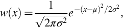
where μ, σ are the mean and variance, respectively. Shot noise is generated by the discrete nature of electrons. This form of noise is modeled as a Poisson distribution. 1/f noise or pink noise is widely observed in nature but its physical basis is poorly understood. As its name implies, its power spectral density is proportional to 1/f.
Thermal noise is inherent in physical systems. In electronic systems, this form of noise in conductors is known as Johnson noise or Johnson-Nyquist noise. This form of noise depends on the resistance of the component and is defined as a power spectral density per hertz of bandwidth:
where k is Boltzmann's constant, T is temperature in Kelvin, and R is resistance in Ohms. Since this formulation results in an infinite noise power level over an unbounded bandwidth, we define the noise relative to the bandwidth of interest in the circuit.
We sometimes want to generate noise. As one example, music synthesizers use random noise as input to synthesizer functions to create more natural sounds. We can generate noise either using analog or digital methods. In the case of digital methods, we often use pseudorandom algorithms that are deterministic but create sequences of outputs that obey a desired distribution. A common approach is to first generate a uniformly distributed sequence and then shape the sequence to the desired distribution.
We will use the term interference to refer to an unwanted signal that comes from outside of our circuit of interest. Interference may come from another part of our circuit or from a completely outside source. Designers have to worry both about generating interference and dealing with interference from other devices. Depending on their application, some circuits may require certification by the Federal Communications Commission (FCC) or other regulatory bodies.
Radio frequency interference (RFI) results in both digital and analog circuits. The wires and electrical leads in electronic systems act as antennas that can both emit radio signals caused by the signals that flow through them and can pick up signals emitted by other electronic systems. We are particularly concerned with RFI at higher frequencies. The optimum length of an antenna to receive a signal is inversely proportional to the frequency of the signal; as a result, short wires are better at transmitting and receiving high frequencies. Digital signals are prone to emitting RFI because logic transitions contain significant spectral components in the megahertz range. We can reduce RFI by shaping digital signals to reduce their rise/fall times. Analog circuits can also generate and receive RFI. Audio signals are at low frequencies that are less prone to interference but other types of analog circuits may operate in bands that allow them to create significant amounts of interference.
We can reduce both emissions and reception by adding shielding. A metal box provides radio frequency shielding; however, even relatively small gaps and holes in the box may leak noticeable amounts of RFI. If we can identify a part of the circuit that is receiving interfering signals, we can use a ferrite bead as a radio frequency choke to prevent the interfering signal from entering other parts of the circuit.
Crosstalk is interference between one part of a circuit and another. Crosstalk typically refers to signals carried by parasitic capacitance and inductance. The mutual capacitance between parallel wires, for example, can provide a path for significant crosstalk currents. We can use capacitance to ground to reduce the effects of crosstalk. Ground is a stable signal and a parasitic capacitance to ground can be used to overwhelm the effect of parasitics to other signals. We often construct a ground plane on circuit boards to help control crosstalk.
4.11 Example: Amplifying an Electret Microphone
Electret microphones [51] are widely used to pick up audio signals. The microphone itself uses permanently charged capacitor plates, one of which is flexible; audio waves that hit the microphone diaphragm cause the capacitor plate spacing to change, resulting in a change in capacitance that follows the sound pressure level.
A typical electret microphone is packaged with a transistor to provide gain as shown in Fig. 4.27. The transistor is configured in a common source configuration. However, the microphone needs external power to provide a useful signal.

Fig. 4.28 shows a simple amplifier for an electret microphone based on an op amp [12]. R1 provides the bias current required by the microphone package. C1 decouples the op amp input from the microphone at DC. R4, R5 form a voltage divider to provide a reference voltage for the op amp. R2 provides feedback across the op amp and its value determines the gain; C3 shorts at high frequencies, rolling off the op amp response. C3 decouples the op amp from the output while R5 discharges C3 to prevent charge buildup.

To choose the values, we need to know the current drawn by the microphone, both AC and DC. The data sheet for microphones typically quotes a sensitivity value in dbV, or the voltage generated at 1 Pascal of air pressure. From that value, we can find the current produced by the microphone given the impedance used to make the sensitivity measurement.
A typical value for the maximum AC microphone current Isp—the current generated by an audio input—is in the tens of microamps. A typical maximum output voltage level for input to audio equipment would be about 1.2 V. The value of R2 is

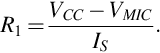
The value for R1 is set to provide the required DC bias current Imic to the microphone, as given in the data sheet. We also need to know the microphone operating voltage VMIC:
We want the R4, R5 voltage divider to produce an output in the middle of the power supply voltage range to provide equal sized swings in both directions. As a result, R4 = R5. This voltage divider does not need to draw large amounts of current so we can use large-valued resistors.
We can choose a value for C1 similar to the approach we used in Eq. (4.10), with the selected corner frequency that cuts off only very low frequencies, for example, fc < 10 Hz.
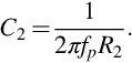
The feedback capacitor C2 helps to stabilize the op amp and forms an RC filter with R2. We want this filter to roll off at a frequency fp high enough to pass the desired audio band. Since R2 and C2 are in parallel, we can determine C2 based on R2 and the cutoff frequency:
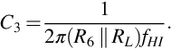
The coupling capacitor C3 is designed with a high cutoff frequency fHI to allow audio signals to pass through. It forms an RC filter with the parallel combination of R6 and the load impedance RL:
Further Reading
The ARRL Handbook [5]is a compendium of information on circuit design; the ARRL RFI Book [24] discusses radio frequency interference in detail. IC Op-Amp Cookbook [32] provides a comprehensive guide to op amp circuits. Prof. Marshall Leach of Georgia Tech was a highly regarded expert on analog and audio system design; his course Notes and papers can be found at https://leachlegacy.ece.gatech.edu.
Questions
- Q4.1 Show the boundary between the linear and saturation regions for this set of MOSFET characteristic curves.

- Q4.2 An amplifier input has a 100 Ω resistance in parallel with a capacitor C. What value for C gives the RC series a − 3 dB cutoff frequency of f = 20 Hz?
- Q4.3 Draw a schematic for a small-signal pi MOSFET model of a source follower amplifier.
- Q4.4 A MOSFET has
 . Find its small-signal gain when used in a common source configuration with RS = 1 kΩ, RD = 200 Ω.
 - Q4.5 An inverting opamp has a feedback resistor R2 = 5000 Ω. What value should the input resistor R1 have to give a gain of − 10?
- Q4.6 Prove that for equal resistor values R = R1 = R2 = R3 = R4, the output of the op amp difference amplifier is proportional to VB − VA.