
Logic
Abstract
Embedded system interfacing often requires us to mix and match components, exposing incompatibilities. In these cases, an understanding of the circuit characteristics of logic is essential to ensuring that the logic works as intended. This chapter reviews CMOS logic characteristics. Logic levels, current drive capability, and timing are critical requirements for interfacing logic. Design examples include open-collector and high-impedance interfaces and a shaft encoder.
Keywords
Digital logic; CMOS; MOSFET; LED; Logic levels
3.1 Introduction
Logic design is a critical component in embedded interfaces. When we design logic using components that have been designed to work together, we can concentrate on their logical function. But interfacing often requires us to mix and match components, exposing incompatibilities. In these cases, an understanding of the circuit characteristics of logic is essential to ensuring that the logic works as intended.
The next section discusses specifications for digital logic. Section 3.3 introduces CMOS logic, based on MOSFETs, and its circuit characteristics. Section 3.4 introduces the high-impedance output gate. Section 3.5 looks at two structures for busses: open drain and high impedance. Section 3.6 discusses registers used to hold state. Section 3.7 examines programmable logic devices. Section 3.8 looks at logic structures we use to connect to CPUs. Section 3.9 discusses steps we must take to protect logic circuits from both electrostatic discharge and noise. Section 3.10 discusses common auxiliary devices such as LEDs. Section 3.11 designs a simple shaft encoder.
3.2 Digital Logic Specifications
The most basic specification for a digital logic circuit is its logical function. Function is specified as Boolean formulas in the case of combinational circuits—logic with no internal state. A state transition diagram or register-transfers can be used to specify sequential machines.
However, a practical digital logic circuit must meet other specifications. Those nonfunctional specifications are the primary concern of this chapter.
Timing is a key parameter for interface logic—the interface may not produce the right functional result if its logic does not meet certain timing parameters. Timing parameters come in several forms:
- • Delay from a specified input to a specified output.
- • Relative timing from one signal event to another signal event.
Bus operations are often specified using timing diagrams as shown in Fig. 3.1. Signals in the timing diagram may be given either as absolute values or as stable/changing regions. The arrows in the timing diagram specify timing constraints—one event must occur before another. If an event is labeled with a time value, the second event must occur at least that period of time after the first event. We will study some important timing parameters for registers in Section 3.6.

Logic signal levels are also related to the proper functioning of logic. Some logic families define signal requirements relative to voltages, others to currents. If the input to a logic gate does not meet the required signal levels, the gate will not produce the correct logical output signal. We will study logic signal levels in Section 3.3.
Power consumption is often specified as a maximum value. The logic must live within the available power from the power supply.
3.3 CMOS Logic Circuits
A logic family is a circuit technology that can be used to create many different types of gates: inverter, NAND, NOR, etc. Most logic today is based on CMOS logic families based on MOSFETs.
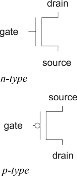
Fig. 3.2 shows two types of CMOS transistors. CMOS transistors are MOSFETs; the C stands for complementary. The two types of transistors provide opposite polarities: when a gate voltage is applied, it enables current to flow between the source and drain. The n-type transistor conducts when its gate voltage is positive while the p-type transistor conducts on a negative gate voltage. Both of these devices are known as enhancement mode because current increases with larger gate voltages. (Depletion mode transistors conduct less current as their gate voltage increases. Some logic families use depletion transistors but standard CMOS uses only enhancement devices.) The gate terminal is capacitive and has a high input impedance.
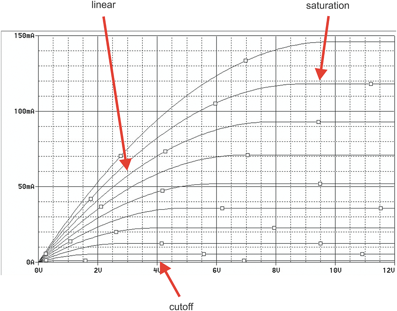
The characteristic curve plot of Fig. 3.3 shows the drain current as a function of drain-source voltage for several different gate-substrate voltages. At each gate voltage, no current flows below a threshold voltage. When the gate voltage crosses the threshold, the drain current increases in the linear region until it peaks in the saturation region. We will study MOSFET characteristics in more detail in Chapter 4.
Logic gates are amplifiers but highly nonlinear ones. We will discuss linear amplifiers in Chapter 4, which we use for amplifying signals while preserving their details. Logic gates are designed to provide reliable digital values by taking advantage of nonlinearity.
Fig. 3.4 shows the schematic for a CMOS inverter built from one n-type (the pulldown M2) and one p-type (the pullup, M1) transistor. The schematic also shows a capacitor connected to its output as a load. The input is connected to the gates of both transistors. (Unfortunately, we use gate to refer both to a logic gate and a transistor gate.) The source of each transistor is attached to a power supply terminal, VSS for the n-type and VDD for the p-type. The gate voltage is measured relative to that power supply level. When a high voltage is applied to the input, M2 is on (high Vgs) and the p-type is off (low Vgs). As a result, M2 discharges the load capacitor. If a low voltage is applied to the input, M2 is off and M1 is on, charging the load capacitor.

Given this basic understanding of how these logic families work, we can set up a scenario in which each logic families fail. CMOS is sensitive to fanout—the number of gates attached to the output of a driver gate. Fig. 3.5 shows a NAND gate whose output is connected to three other gates; this connection is sometimes called a fanout tree. The mechanisms by which they fail are different thanks to the different operating characteristics of the families. Fanin is the number of gates connected to the input of a given gate; some logic families are also sensitive to fanin constraints.

Capacitance is at the root of the fanout problem. In practice, the load capacitance is the gate capacitance of the transistors that form the next logic gate. As fanout increases, the capactive load increases. As shown in Fig. 3.6, we can model this situation with a current source for the driver gate's output and a capacitance for the load. One of the driver gate's transistors is on and operates in its saturation region. The input capacitances of the load gates are in parallel so we can add them to find the total load capacitance. The voltage across this capacitance is equal to the input voltage at each fanout gate; all fanout gates see the same input voltage. That voltage waveform is simple—a ramp until it reaches the power supply voltage, at which point the driver transistor turns off. The slope of the ramp depends on the ratio of the load capacitance and the driver current:

The output current is determined by the logic family. As the load capacitance increases, the slope decreases and the time required for the voltage to reach its final value increases. Interfaces have timing requirements—a maximum delay from the change of an input to the change at its output. If the slope of the voltage waveform is shallow enough, the logic fails to satisfy its timing requirement.
Given these illustrations of the importance of electrical specifications to the proper function of logic gates, we can now look at the specifications themselves. Most logic families represent logic values as voltages; a few logic families use currents to represent logical values. We talk informally about a high voltage representing a logic 1 and a low voltage representing a logic 0. In fact, a range of voltages can be used to represent logic values. Accepting a range of signal values protects the logic functions against noise, which is inevitable in real circuits. Intermediate values represent invalid logic values, which we often refer to as X. Leaving a gap between the valid logic 0 and logic 1 levels also contributes to noise immunity. Without an X value in between, a small amount of logic would flip the logical value. If noise pushes a valid logic value into the X range, we can at least detect that the value is invalid.
The data sheet for each component is a critical part of your design: without a data sheet, you don’t know the component's characteristics. The data sheet for a logic gate or family specifies characteristics of input and output signals: for input signals, the required voltages and currents to signal a valid logic value; for output signals, guarantees on the signals that the output generates. Fig. 3.7 illustrates the relationships between logic levels when one gate drives another. The highest voltage that represents a logic 0 is VOL; the lowest input voltage that represents a logic 0 is VIL. If VIL < VOL, we know that any valid logic 0 produced by the output gate will be interpreted as a logic 0 by the next gate. Similarly, if VOH > VIH, we are guaranteed that any logic 1 produced by the output gate will be treated as a logic 1 by the input gate. The high and low ranges do not have to be the same and the input and output ranges do not have to be equal.
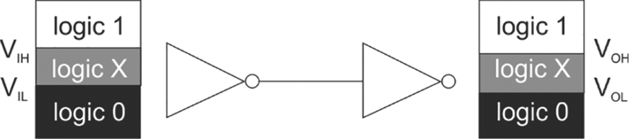
Fig. 3.8 shows some of the specifications from a data sheet for a CMOS NAND gate. CMOS logic can operate over a wide range of voltages. The input voltages VIL, VIH and the output currents IOL, IOH are both specified. CMOS output voltages asymptotically approach the power supply voltages so their worst-case levels do not need to be specified.

If we mix logic from two different logic families, we need to be careful to obey the input and output signal specifications. These specifications also limit our ability to connect logic gates to nonlogic circuits. For example, a logic gate may not be able to supply enough current to directly drive a speaker.
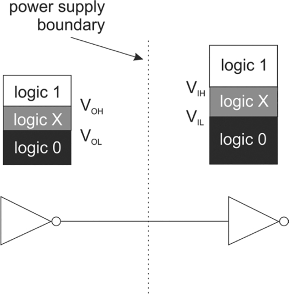
If we mix logic that operates at different power supply levels, we also need to be careful about signal levels. Many digital systems use multiple power supply voltages, which they use to trade off power consumption and performance. Since the range of valid logic 0 and 1 voltages depends on the power supply voltage, changing power supply levels leads to changing the range of valid logic values. As illustrated in Fig. 3.9, if we connect the output of a gate at a low power supply voltage to the input of another gate at a higher power supply voltage, a voltage produced by the first gate as a logic 1 may be too low to be interpreted as a 1 by the next gate; instead, it could be treated as a logic X.
3.4 High-Impedance and Open-Drain Outputs
Some logic gates offer another form of output, known as high impedance, three-stating, or tri-stating™. Three states are useful in connecting gates together to form a bus. Fig. 3.10 shows two three-state gates connected to a bus. Each gate has its data input as well as an enable input: if enable = 1, the gate's output is the inverse of the data input; if enable = 0, the gate's output is set to high impedance. We often refer to the high impedance output value as Z. We can select which gate writes its value on the bus by setting the values of the two enable inputs. Of course, if both gates are enabled, they will both be electrically connected, which is particularly bad when the data values are different. Not only can this cause a bad logical value to appear on the bus but it may damage the circuits due to large short circuit currents.

Fig. 3.11 shows a CMOS inverter with a three-state output. The inverter's output is guarded by n-type and p-type transistors M3, M4. When enable = 0 (and enable’ = 1), both of these transistors are off, defeating both M1 and M2. When enable = 1 and enable’ = 0, both transistors are on and the pullup and pulldown transistors can effectively determine the proper output value.

Some logic families do not include a pullup device or resistor. Instead, the bus or external connection is connected to a pullup resistor R1 as illustrated in Fig. 3.12. Pulldown transistors inside the gates will, when turned on, cause the bus voltage to go low. If no gate tries to pull the bus voltage down, the pullup maintains the bus at a high logic level. The MOS version of this circuit is known as open drain since the transistors’ drain connections are left unconnected.

In the case of TTL, this configuration is known as open collector. The maximum current supplied by the pullup resistor must be no larger than the maximum sink current of one gate and the current flowing from the inputs of the n fanout gates [58]:

3.5 Example: Open-Drain and High-Impedance Busses
Busses are common connections that are used for data communication between various combinations of devices. Only one device at a time may write the bus. The destination for the data may be one or several devices. We can use two different circuit families to design busses with different characteristics.
We can use pullup resistors to build busses that allow easy connection and disconnection of devices. If the transistors used on the bus are bipolar, we refer to the bus as open collector; if the transistors are MOSFETs, the bus is open drain. A classic example of the open-drain/open-collector bus is I2C, which we discussed in Section 2.3.
Fig. 3.13 shows an open-drain bus circuit. The bus is a wire connected to pullup resistor Rpu. Each module on the bus has a pulldown transistor M1, M2, etc. If any of the devices turns on its pulldown transistor, the bus voltage is pulled to a low voltage. If no modules are on, the bus is kept at a high voltage thanks to the pullup resistor. If two modules turn on their pulldown transistors, the bus continues to operate normally. Open-collector and open-drain busses are robust because they are insensitive to multiple devices writing on the bus. However, the pullup transistor causes the bus to be relatively slow.
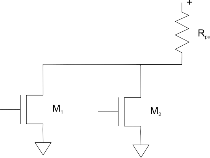
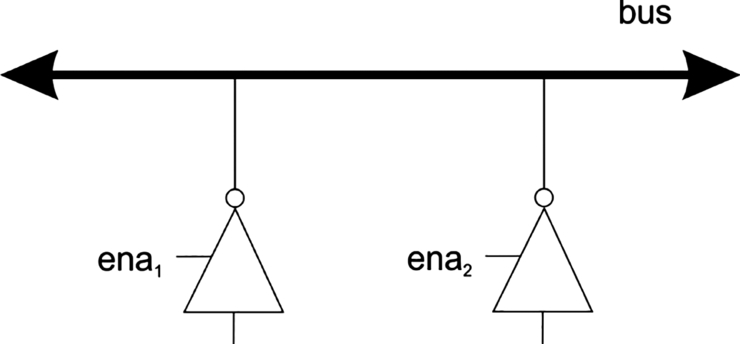
Fig. 3.14 shows a high-impedance bus. Consider first a bus that is only a wire without a pullup resistor. Each module uses a three-state gate to connect to the bus. (We use inverting gates here but the polarity of the bus logic is not important to its circuit characteristics.) If one three-state gate is enabled, it controls the value on the bus. If two three-state gates are enabled and they output the same value, the bus continues to operate. If the two gates have opposite values, they will fight each other, resulting in at least a bad logic value on the bus and perhaps damage to the circuits. If no three-state gate is enabled, the bus is floating and does not have a reliable digital value. We can use a weak pullup to keep the bus at a valid logic value; the pullup is chosen to provide a small enough current that if a three-state gate can overcome it and determine the bus value.
3.6 Registers
We use the term register for any type of circuit used to locally store a bit value.
The simplest type of register is the SR latch, shown in Fig. 3.15. This latch does not have a clock input. Instead, its internal value is determined by the values of the set (S) and reset (R) inputs. SR latches are not widely used today because they may not reliably capture the intended value. SR latches made by hand from a pair of NOR or NAND gates are particularly unreliable—the parasitics of wiring affect the behavior of the latch too much.
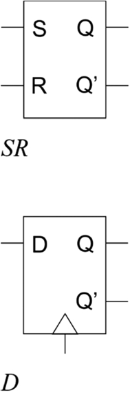
Clocked registers are more reliable: a clock input determines when the data input value is read. The D register, also shown in Fig. 3.15, is one form of this type of register; other options also exist. Two major variants on the relationship between the clock and the internal state exist. A level-sensitive register, which we refer to as a latch, reads the data input into the register state so long as the clock signal is enabled. Once the clock signal is disabled, the internal state conforms to the last state on the data input. We call this form of register transparent. An edge-triggered register, which we refer to as a flip-flop, loads the register value only in a narrow interval around a clock edge.
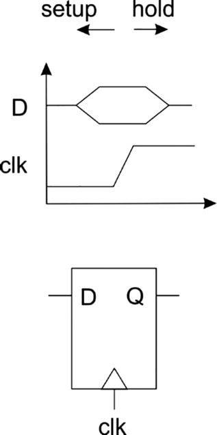
Both types of registers must obey two timing constraints setup and hold times. Fig. 3.16 shows these timing requirements for the case of a positive edge-triggered registered. The setup time ts is the time before the clock edge during which the data input must be stable. The hold time th is the time after the clock edge during which the data input must remain stable. In the case of a level-sensitive register, these times would be measured relative to the end of the active clock. If the data signal does not obey the setup and hold times, the register may store the wrong value. These times are often quoted as a combined setup-and-hold time.
A register's performance is given by its propagation delay from input to output: tPLH for low-to-high transitions and tPHL for high-to-low transitions.
Setup-and-hold time is an important design constraint because all registers can suffer from metastability. If the data value changes around the clock event, then the register may store an intermediate X state. As shown in Fig. 3.17, the register will eventually settle to a valid logic value but the time to do so is random and can be extremely long. When it does settle, it may settle on the wrong value. This phenomenon is often compared to a ball poised at the top of a hill; it may sit at the top for quite some time before a random wind blows it to one side of the hill or the other. We cannot eliminate metastability, we can only minimize it. Metastability is a particular concern when a register connects two regions that operate on different clocks—in this situation, some fraction of the inputs will inevitably fall in the metastability danger window.

We compute the probability of a metastable output based on a settling time S. The register has a time constant τ and setup/hold time tSH. We also need to know the clock period. The probability of a metastable output failure at the end of the settling time is
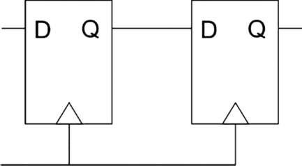
The double-register structure of Fig. 3.18 is often used to minimize the effect of metastability. The logic must be designed to take into account the extra clock cycle of delay. The two levels of register give the signal extra time to settle. The signal may settle to the wrong value, and there is still a chance that the second register may end up with an X. Occasionally, three levels of register are used to further reduce the chance of saving a metastable value.
3.7 Programmable Logic
We often need to design glue logic to perform basic operations in the interface. While small-scale integrated (SSI) circuits may be useful in some situations, chips that can implement more logic are often useful. Complex programmable logic devices (CPLDs).
A field-programmable gate array (FPGA) can implement multilevel logic—logical functions of varying depth. The two basic elements in an FPGA are programmable logic and programmable interconnect. A programmable logic element can be configured to represent a given logical function; typically an element has a limit on the number of inputs it can handle but can compute any logical function within that range of inputs. Programmable logic elements also include registers to store values. Programmable interconnect can be configured to make connections from the output of one logical element to the input of another. The most common means of configuring an FPGA uses static RAM (SRAM). Since SRAM loses its values when the power supply is removed, the FPGA must be configured whenever it is powered up. A configuration file is loaded into the FPGA to set the configuration of the logic elements and interconnect; specialized memories can be used to automatically load the configuration into the FPGA. We often refer to the configuration process as programming but this process is very different from programming a computer—an FPGA does not fetch and execute instructions.
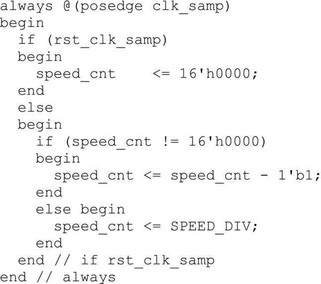
We create a configuration file using computer-aided design (CAD) tools and hardware description languages (HDLs). Fig. 3.19 shows a simple HDL description in the Verilog language; VHDL is the other major hardware description language. CAD tools first optimize the logic design, then determine where to place functions into logic elements and how to route elements between the logic elements. The result is a configuration file.
Programmable logic demands programmable I/O pins. FPGA and CPLD pins can be configured as input, output, or high impedance. Other aspects of the pin may also be configured. A common example is slew rate—the speed at which the output changes from 0 to 1 or 1 to 0. Fast signals demand high slew rates but signals that do not need to be fast can use a slow rate to reduce power consumption and electromagnetic interference.
Many advanced FPGAs are organized as a system-on-chip (SoC). In addition to a fabric of programmable logic elements and interconnect, they provide embedded memory, multipliers, one or several CPUs, and specialized I/O subsystems such as Ethernet.
3.8 CPU Interface Structures
CPUs may provide any of several different types of logic structures as interfaces to the CPU itself.
General-purpose I/O (GPIO) is a set of pins that are uncommitted to a particular purpose. GPIO pins can usually be configured to be either an input or an output.
Some microprocessors expose a bus to system designers, either their main bus or a bus specifically designed for I/O. The bus operates a protocol that determines what actions are taken by each device on the bus. The bus has a master that initiates operations. By default, the CPU is the master. The bus may provide a bus request signal to allow another device to temporarily become bus master.
Busses require different devices to drive some signals at different times—the CPU and memory, for example, may each write data onto the bus at different times. High-impedance or common drain/emitter circuits are often used at bus interfaces.
A simple example is shown in Fig. 3.20, which gives a timing diagram for a bus read operation. (Read/write directions are relative to the CPU when describing CPU busses.) The bus master presents an address on adrs and asserts address ena; the signals are timed to be valid before the rising clk edge. When the device is ready, it asserts data and data ready. In this simple protocol, the data is asserted for one clock cycle; some protocols may use a signal for the CPU to assert when it has captured the data.
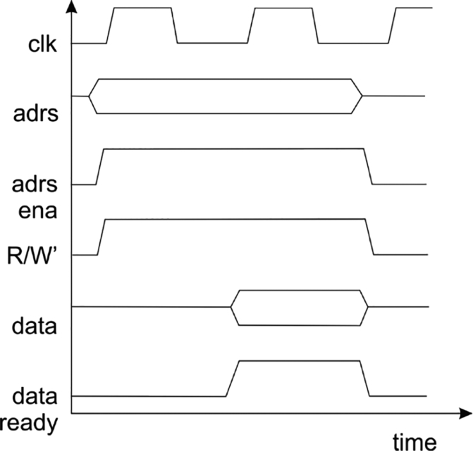
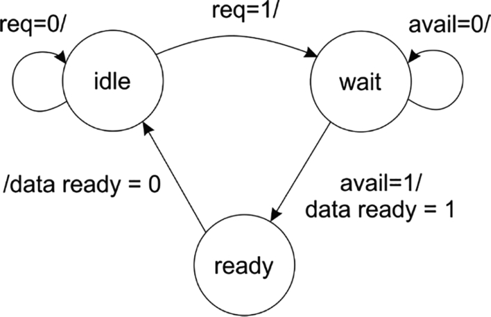
Fig. 3.21 shows a logic schematic that provides the device's responsibilities for this protocol. The interface is designed to wait for the data to arrive from the interior of the device as signaled by avail. The cmp block compares the adrs value to the device's value. A protocol FSM controls the operation of the bus-side logic.

Fig. 3.22 shows the state transition diagram for the protocol FSM. When req is asserted, the FSM waits for a data input from the remainder of the device. When that data is ready, the machine asserts data ready for one clock cycle to signal the bus master.
3.9 Logic Protection and Noise
Logic requires two types of protection from the outside world and from itself: static electricity and electromagnetic interference (EMI).
CMOS logic is particularly sensitive to static electrical discharge. The gate oxide of a MOSFET is necessarily thin. Large voltages from static discharge can breakdown the MOSFET, rendering the circuit inoperative. When working on circuits, we should connect ourselves to ground using a ground strap.
The electrical signals on any wire generate electromagnetic fields. Wires also act as antennas that can receive the electromagnetic signals around them. We need to take steps to minimize both the EMI generated by circuits and the effect of EMI on our circuits. Reducing the slew rate of signals is an example of an active method of EMI minimization. Shielding—putting circuits in a metal box—both prevents generated EMI from being transmitted to the environment and protecting the circuits from external sources of EMI. We will discuss noise in more detail in Section 4.10.
Power supplies are an important source of noise for digital circuits. We have seen that our circuit models for logic gates depend on power supply voltages. Violating the power supply requirements will inevitably cause problems. We can reduce power supply noise, often called power supply ripple, using decoupling capacitors that is placed between the VDD and VSS power supply connections. Each decoupling capacitor serves a particular set of logic. As shown in Fig. 3.23, we may place decoupling capacitors at several points in the circuit. In many cases, we add a separate decoupling capacitor at each significant integrated circuit. The decoupling capacitor acts as a low-pass filter on the power supply; we can also view it as a charge reservoir for short-term use when the logic's current draw becomes too high for the power supply. Given logic current for n gates of nImax and a maximum power supply ripple of △ V over an interval tmax, the required decoupling capacitance is [74]:

3.10 Auxiliary Devices and Circuits
The light-emitting diode (LED) is a common and very useful output device. Not only is an LED a useful indicator for the end user, but it can also be used during debugging to indicate signal state. Wiring an LED to a logic signal is straightforward but requires a little care. As shown in Fig. 3.24, the LED is connected in series with a resistor. The LED's orientation allows current to flow from the positive supply to ground. We can control the LED with the logic signal by using the logic signal as the positive terminal for the LED/resistor assembly. The current supplied by the driving logic gate determines the brightness of the LED. The resistor's role is to regulate current and provide a voltage drop. The LED's voltage is 0.7 V when it is on. The remaining voltage drop between the power supply terminals occurs over the resistor. We choose the value for the resistor based on the desired voltage drop and the current available from the driving gate:

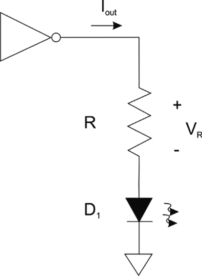
Unless we need a particularly bright LED, we probably want to use a value for Iout lower than the data sheet maximum in order to avoid overstressing the driving gate.
The optoisolator combines an LED and a photosensitive transistor (in this case, a bipolar transistor) to create a logical signal path with no direct electrical connection. Fig. 3.25 shows the schematic symbol for an optoisolator. The output transistor's base acts as an optical detector; light from the input LED determines the output transistor's emitter-collector current. Optoisolators can be used to provide separate power supply circuits for different parts of the circuit, isolating one from the noise in the other circuit. As we will see in Section 3.11, we can use an optoisolator as a detector.

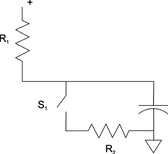
Switches are often used for input. We have to take the mechanical characteristics of the switch into account within the interface. When a switch is closed—the contacts are pushed together to make a connection—the metal contacts bounce several times. As shown in Fig. 3.26, the switch will open and close many times in a short interval before it settles to its stable, closed value. We do not want to send all these events as a string of 1s and 0s to the CPU. Instead, we want to debounce the switch—temporarily force it to a single value until it settles. Of course, we want the user to be able to open the switch and turn off the connection. Given the short time scale of switch bouncing, the user does not observe any delay in being able to reopen the switch. We can any of several techniques to debounce a switch. We can do so in software using a CPU timer. At the other end of the spectrum, we can use the circuit in Fig. 3.27. When switch S1 is open, R1 charges C1, providing a stable value logic 1 on the output. When the switch is closed, C1 is drained through R2, bringing the output voltage to a low level. We can easily manage the sense of the switch (logic 1 means open switch) in software.

A third option is a debouncer based on an integrated circuit known as a one-shot. The one-shot, also known as a monostable multivibrator, responds to a transition on its input by setting its output high for a given amount of time. At the end of the pulse, the one-shot’s output returns to its original state. The length of the pulse is determined by a capacitor. By ORing (or NORing) together the raw switch signal with the one-shot pulse, we can smooth over the switch bounces. We will discuss one-shots in more detail in Section 5.10.
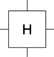
A Hall effect sensor uses the interaction of magnetic fields and electric currents to detect the position of a magnet. Fig. 3.28 shows the schematic symbol for a Hall effect sensor. S magnetic field H imposes a force on an electric current I. The force causes the current t deflected, changing the voltage across the sensor. The Hall effect produces a linear variation in voltage from the magnetic field which we can use either for fine position of a magnet or as a nonlinear detector. For example, Hall effect sensors are commonly used to detect whether car doors are open or closed: a permanent magnet is placed on the door and the sensor body is placed in the door frame. The sensor reading indicates whether the magnet is next to the sensor—the door is closed—or whether the magnet is away from the sensor—the door is open. Hall effect sensors are also used in brushless DC motors to detect the position of the motor shaft.
3.11 Example: Shaft Encoder
We often need to detect the movement of a shaft: knobs on equipment turn shafts that are intended to control the equipment's operation; the position of a servo motor needs to be determined as an input to control. The optical shaft encoder is widely used thanks to its superior characteristics compared to mechanical or electromechanical alternatives: it provides low noise and low friction at a low cost.
Fig. 3.29 shows a simple shaft encoder. The shaft, made in this case from a paperclip, is fitted with a target of alternating white and black areas. That target is positioned in the middle of a variation of an optoisolator known as an optical detector or a reflective optical switch. This device points its LED output outward and provides a lens to capture reflected light. The target modulates the light that is reflected from the LED to the photodetector. The white and black areas of the target reflect different amounts of light depending on the position of the shaft. The output of the photodetector produces a signal that indicates when the target has been rotated from one area to the next. Optical detectors come in several configurations of the emitter and detector: parallel to each other, pointed at each other, and in this case reflected at an angle. These different arrangements are suited to different physical environments.
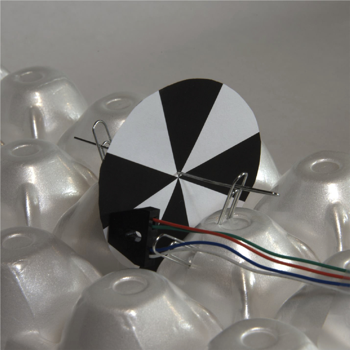
Fig. 3.30 shows a simple pattern for the target. The alternating black and white regions allow the detector to determine when the shaft has moved from one region to another; we can increase the resolution of the encoder by dividing the target into narrower slices. However, this target pattern gives us only a relative position for the shaft. The pattern of Fig. 3.31 encodes a three-bit position over the radius of the target (the white spacers between the target patterns were inserted for clarity and are not strictly necessary). We can use three optical detectors to read the three bits of the position. Those bits give us enough information to determine which direction the shaft has turned and its absolute position to within 45 degrees. More tracks to the pattern and more detectors allow us to measure position more precisely. We can also add a separate track with a fiducial mark at a fixed position to provide a reference. This target uses a standard binary up-down code; a Gray code provides protection against mis-reads and glitches.


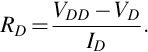
Our setup uses the OPB703WZ detector [72]. Fig. 3.32 shows the schematic for the detector circuits with the colors of the leads from the detectors as shown. We need to choose the values of the two resistors: RD determines the amount of light produced by the LED; RT determines the output current of the photodetector for a given amount of light. If the LED produces too much light for the photodetector, the detector's output will always be on; if the LED produces too little light for the photodetector, the detector will always be off. The two resistor values are related: the ratio RD/RT determines the relationship between LED output and photodetector sensitivity. The data sheet gives us some guidance to the proper resistor values.
- • The LED forward DC current is ID = 40 mA at a forward voltage of VD = 1.7 V.
- • The phototransistor collector DC current is 3.5 mA at an emitter-collector voltage of 5 V.
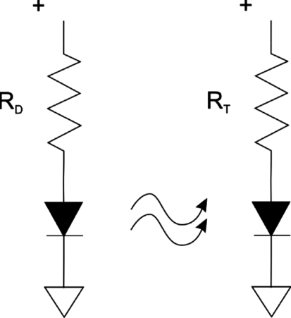
Once we choose the power supply voltage, we can find
On the output side, we need to check two conditions: the logic 0 output value produced by the photodetector is compatible with the next stage of logic; and that the on current produced by the photodetector is sufficient to drive the next stage.
Further Reading
Wakerly [73] provides a thorough introduction to logic design.
Questions
- Q3.1 A CMOS gate has a maximum current of 4 mA at a power supply voltage of 5 V. Given an LED on voltage of 0.7 V, what value of resistor should be used if we want to draw half the maximum allowable current to light the LED?
- Q3.2 An LED is driven by an inverter to display a logic value. The inverter can supply a maximum output current of 2.5 mA. The power supply voltage is 3.3 V. What value of resistor should be used to draw an on current of half the inverter's maximum rating?
- Q3.3 An LED is driven by a series 5 kΩ resistor. Given a power supply voltage of 3.3 V, what is the diode current?
- Q3.4 What conditions govern the value of a pullup resistor for an open-drain connection?
- Q3.5 A CMOS gate operates at VCC = 3.3 V, VIH = 3.15 V, VIL = 1.35 V. How much drive current must the gate provide on a 1 → 0 transition to a gate with input capacitance of 15 pF to achieve a delay of 10 ns?
- Q3.6 A CMOS gate rising input follows an exponential curve with time constant τ = 3 ns. The gate operates on a power supply of 3.3 V. If the logic levels are VIH = 3.15 V, VIL = 1.35 V, how long is the gate input in the unknown region?
- Q3.7 A CMOS logic family has an input capacitance of 15 pF and an output current of 20 mA. It operates at a power supply voltage of 3.3 V. What is the maximum fanout to ensure transition times less than 15 ns?
- Q3.8 Draw a timing diagram for the operation of a D register. The timing diagram should include a setup time of 20 ns and hold time of 7 ns.
- Q3.9 A register has a time constant of τ = 3 ns, a setup/hold time of tSH = 27 ns. Its input clock has a period of 50 ns. How long must it be given to settle to ensure a metastability probability below 10− 20?
- Q3.10 A CMOS logic family draws current of 10 mA at a power supply voltage of 3 V. You are given a block of logic with 20 gates. How much decoupling capacitance is required to ensure a maximum power supply drop of 10% over 5 ns?
- Q3.11 Design a modified form of the bus interface of Section 3.8 that allows for variable timing of the register read.
- (a) Modify the timing diagram to use a data ack signal to acknowledge the read by the CPU.
- (b) Draw a state transition diagram for the FSM.