
Filters, Signal Generators, and Detectors
Abstract
Filters allow us to select and transform signals using linear operations. Detectors perform nonlinear operations to identify events on signals. Signal generators create useful signals. Filters can be built both as passive RLC filters and op amp-based active filters. Signals can be generated using analog or digital methods. Small analog circuits can be used to perform a range of useful detection functions. Design examples include a bass boost filter, arbitrary waveform generator, and headphone jack detector.
Keywords
Passive filters; RLC filters; Active filters; Op amp filters; Digital filters; Pulse and timing circuits; Signal generators; Signal detectors
5.1 Introduction
Circuits operate on signals. We use circuits to generate useful signals, manipulate the signals, and interesting properties. Filters perform linear functions on signal and, for example, allow us to select ranges of frequencies in a signal. Detectors perform nonlinear operators. We will consider passive R, L, and C components; active circuits built from op amps; and digital methods.
The next section introduces the basic forms of specification for filters. Section 5.3 introduces the tank circuit and its properties. Section 5.4 discusses transfer functions; Section 5.5 considers the relationships between filter specifications and transfer functions. Section 5.6 introduces active filters using op amps. We then pause to consider a bass boost filter as an example in Section 5.7. Section 5.8 looks at advanced types of filters. Section 5.9 introduces digital filter structures. Section 5.10 considers pulse and timing circuits. Section 5.11 looks at methods to generate waveforms. Section 5.12 designs a digital arbitrary waveform generator. Section 5.13 introduces some useful detectors. Section 5.14 uses a comparator to determine when a headphone jack is inserted into a connector.
5.2 Filter Specifications
While we can specify and design all sorts of filters, four categories account for many of the filters of practical use:
- • A low-pass filter passes low frequencies and attenuates high frequencies.
- • A high-pass filter passes high frequencies and attenuates low frequencies.
- • A band-pass filter passes intermediate frequencies and attenuates low and high frequencies.
- • A band-reject filter attenuates at intermediate frequencies and passes at low and high frequencies.
In each case, we need to specify two types of regions:
- • The passband is the band in which the filter passes signals.
- • The stopband is the band in which the filter attenuates signals.
The transition band falls between the passband and stopband. We do not explicitly specify the transition band; its characteristics are inferred.
The most basic specification for a filter is a filter specification diagram which is used to describe its amplitude characteristics. An example is shown in Fig. 5.1. This example shows a low-pass filter. The y-axis represents loss—large values mean low output levels. The white areas of the plot are the allowable range for filter response while the gray regions are forbidden regions. The passband is specified by two parameters: Amax is the passband attenuation; ωp is the maximum frequency in the passband. Similarly, the stopband is specified by Amin and ωs. The region in between the passband and stopband is the transition band.

Any particular filter can be plotted on these axes as a line showing that filter's loss versus frequency response. As shown in Fig. 5.2, any response curve that falls in the white area meets the specification; any filter whose response curve enters the shaded areas does not meet the specification.
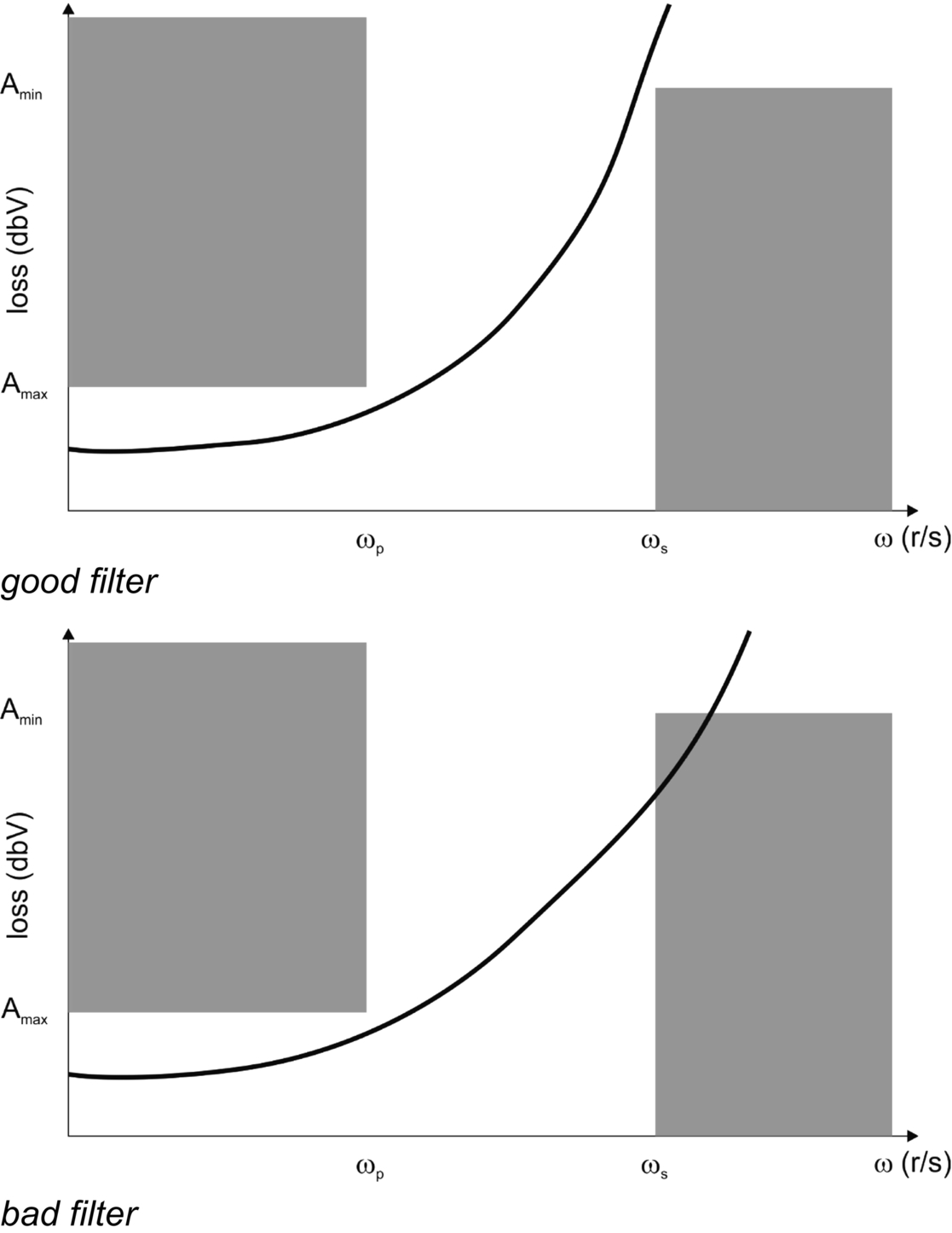
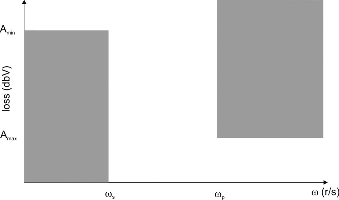
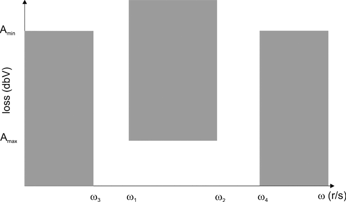
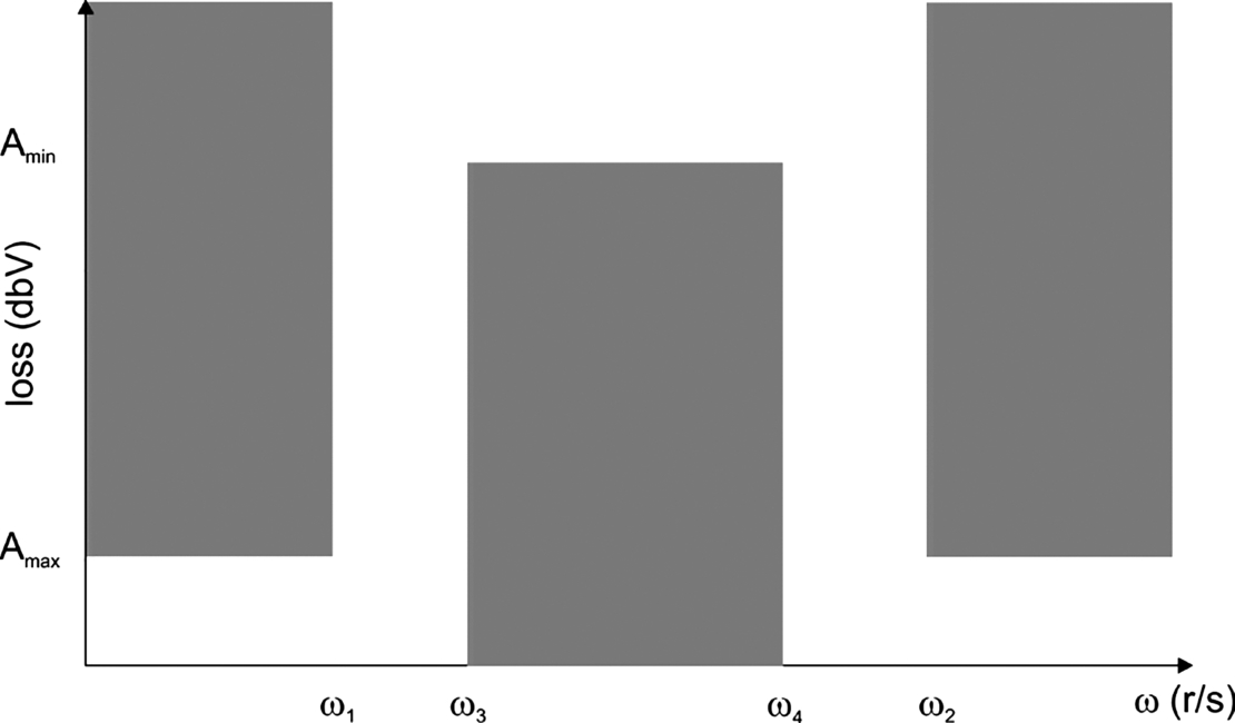
Fig. 5.3 shows an example diagram for a high-pass filter. In this case, ωs < ωp. Fig. 5.4 shows a band-pass filter diagram: the passband frequency range is [ω1, ω2], the lower passband stops at ωe, and the upper passband starts at ω4. Fig. 5.5 shows a band-reject diagram.
Audio applications vary in their application characteristics. High-fidelity audio corresponds to a bandwidth of 20 Hz to 20 kHz. Voice-quality audio corresponds to a frequency range of 20 Hz to 4 kHz.
We may also want to specify the filter's ripple in the stopband, passband, or both. Some filter structures result in a ripped rather than smooth characteristic. Some applications are not particularly sensitive to ripple but in some cases we may want to specify a maximum ripple.
In some cases we may also specify phase delays at various frequencies. Audio applications are generally less sensitive to phase but digital signals can be easily distorted by phase delays.
5.3 The RLC Tank Circuit
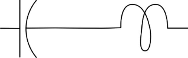
The RLC oscillator, known as the tank circuit, is an important type of passive circuit. Not only is it useful in itself but its characteristics provide us with some characteristics we can use to describe filters.
Fig. 5.6 shows an ideal tank circuit consisting of an inductor and a capacitor with no resistor. The figure shows a series form of the LC tank; we can also build a parallel form. If we provide the circuit with energy—for example, by sending a pulse—the voltages and currents in the inductor and capacitor will oscillate. Because the circuit has no resistance, it does not dissipate energy and the tank circuit oscillates forever.
The formal name for a tank circuit is a resonant circuit. The frequency at which the circuit oscillates is known as its resonant frequency. The resonant frequency in radians per second is

The LC circuit has infinite impedance at its resonant frequency. It appears as an open circuit at that frequency.
Fig. 5.7 shows parallel and series version of the RLC tank. Even if we do not add a discrete resistor to the circuit, capacitors and inductors have parasitic resistances; inductors are particularly prone to parasitic resistance given that they are built from coiled wires.

Fig. 5.8 shows the current and voltage waveforms for the inductor in a parallel RLC circuit. The circuit's resonant frequency is ωr = 6282 r/s or fr = 1 kHz. The waveforms show the largest current at the resonant frequency and lower current values both below and above.

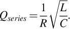
The RLC circuit's resistance does not change its resonant frequency but it does spread out it frequency response. The width of that curve is a measure of the circuit's Q or quality. The Q of a series RLC circuit is
The Q of a parallel RLC circuit is

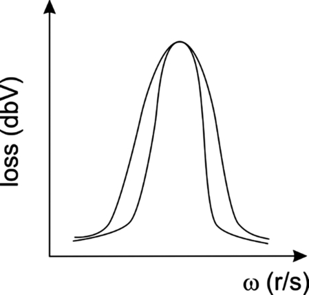
As shown in Fig. 5.9, high-Q circuits have narrow bandwidth curves while low-Q circuits have a wide bandwidth curve. High-Q circuits are very frequency selective while low-Q circuits are less selective. If we think of the tank circuit as a band-pass filter, the high-Q circuit has a narrow passband.
The resonant circuit bandwidth Δ ω is a more direct measure of the width of the frequency response:
As shown in Fig. 5.10, Δ ω measures the separation between the − 3 dB points on the frequency response.

5.4 Transfer Functions
As we saw in Chapter 1, the transfer function is a complete description of a filter's characteristics. We write the transfer function in the s domain. We can define four different transfer functions depending on what we measure at the input and output:
- • The voltage-to-voltage transfer function Vout(s)/Vin(s).
- • The current-to-current transfer function Iout(s)/Iin(s).
- • The transimpedance transfer function Vout(s)/Iin(s).
- • The transadmittance transfer function Iout(s)/Vin(s).
Which transfer function is most appropriate depends on the nature of the source and sink attached to this circuit—whether each is best thought of in terms of voltages or currents.
Our transfer functions will be the ratio of two polynomials:

We can factor the numerator and denominator polynomials to rewrite the transfer function:

This form exposes important structure in the transfer function. The roots of the numerator are known as zeroes because an s-domain frequency equal to one of the root results in a zero value for the transfer function. The roots of the denominator are known as poles because the transfer function becomes infinitely large at those values.
The values of the poles and zeroes determine the shape of the filter in the frequency domain. We place poles to create the passband and zeroes to create the stopband.
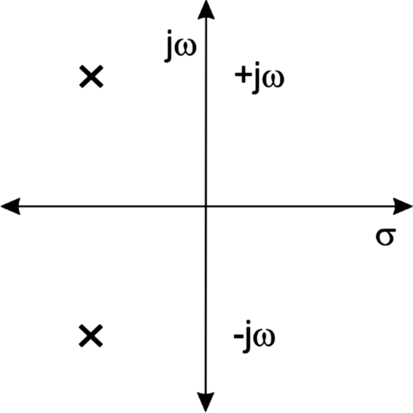
We can draw the poles and zeroes on the complex plane as illustrated in Fig. 5.11. Poles or zeroes on the real axis represent purely exponential behavior; poles and zeroes on the imaginary plane represent purely sinusoidal behavior; poles and zeroes elsewhere represent the product of exponentials and sinusoids. Imaginary poles come in symmetric pairs at ± jω values.
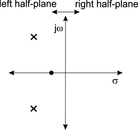
We require that the poles be on the right half-plane—their real component must be < 0. If their real component were greater than zero, the exponential part of their behavior would have a positive coefficient, which in turn means that the function grows with time. Poles in the right half-plane correspond to negative exponentials which tend toward zero at t = ∞. We have no limitation on the position of zeroes—a zero can be in either the left or right half-plane.
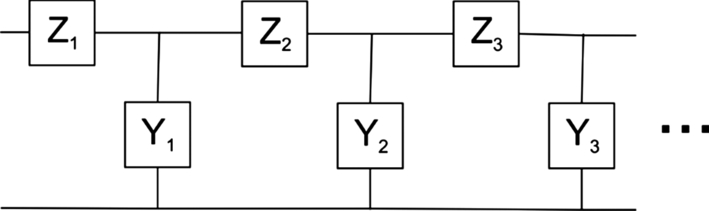
Poles and zeroes have a natural relationship to the physical behavior of the circuit. That relationship is particularly easy to see in a ladder network, shown in Fig. 5.12. A ladder network is built from a cascade of L-shaped elements. It is convenient to think of each element i as being made of one series impedance Zi and a parallel admittance Yi. If the impedance has an infinite value at some frequency ωi then no current flows and the ladder network has a zero at that frequency. Similarly, if the admittance Yi is infinite at some frequency, it shorts the ladder, forming a zero. Conversely, if Zi is zero at some frequency, it forms a pole at that frequency; if Yi is zero at some frequency, it is an open circuit that forms a pole.
While we can create an exact plot of the transfer function, in either magnitude or phase, as a function of frequency, a simple approximation of the transfer function is often enough for many purposes. The Bode plot method, which we introduced in Section 1.4, tells us how to create an asymptotic plot from the transfer function. The form of the body plot also gives us clues as to how to describe the transfer function.
Fig. 5.13 shows magnitude and phase Bode plots for the transfer function


We can construct the asymptotic lines for the plots directly from this factored form, which has a zero at 10 rad/s and poles at 100 rad/s, 10,000 rad/s. The initial term determines the magnitude of the response. Each pole or zero forms an asymptotic line in the Bode plot: a zero forms an ascending line in magnitude and phase; a pole forms a descending line in both magnitude and phase. We create the plot by taking the poles and zeros in order of frequency and building their asymptotes. The slope of each asymptote is 20 dB per decade in magnitude, 45 degrees per decade in phase. If n poles happen to be at the same location, these values are multiplied by n. As we construct the asymptotes from left to right, zeroes and poles change the slope of the asymptotic bound.
When we compare the asymptotes to the exact transfer function, we see that the actual magnitude response is 3 dB below the corner between the two asymptotic lines. If we had multiple poles or zeroes at a given frequency, the response change is multiplied by the number of poles/zeroes. Given the corner frequencies, we can quickly find the points of the frequency response at those points. From there, we can quickly sketch a more accurate representation of the frequency response. On the phase response, the transfer function goes through the asymptote at the pole/zero frequency.
The case of a pair of resonant poles is handled somewhat differently. The pair of complex poles formed by the quadratic s2 + as + b can be formed, for example, by a tank circuit. A shown in Fig. 5.14, the magnitude plot forms a peak at the resonant frequency
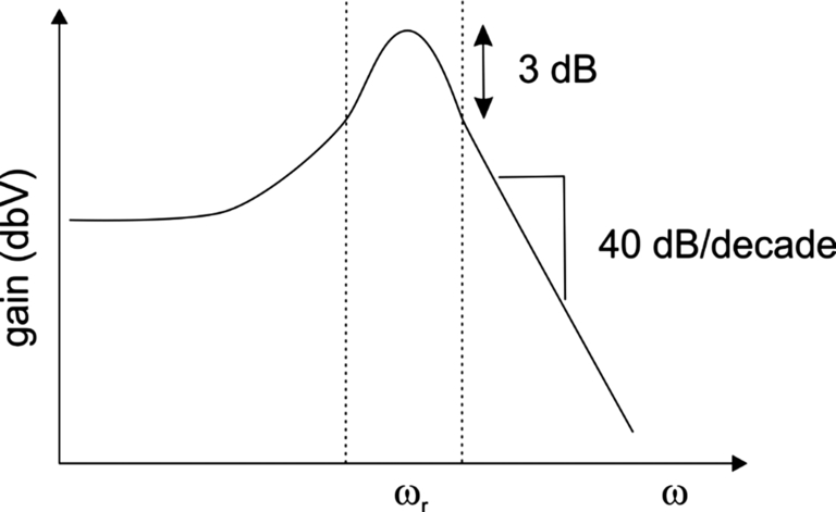
We know from the resonant bandwidth frequency of Eq. (5.4) that the − 3 dB points of the resonant response are related to Q. Those points are located at
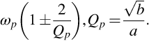
Fig. 5.15 shows the resonant poles on the s plane. Their position on the vertical axis is determined by their frequency with higher frequency poles located farther from the origin. Their distance from the origin on the horizontal axis is related to the degree of damping with lower Q corresponding to a distance farther from the origin.
5.5 From Filter Specification to Transfer Function
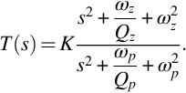
Given a filter's specifications for passband and stopband, we can directly write the transfer function [17].
We will start with basic filters in biquadratic or biquad form to provide the form of the transfer function:

We can recast this in transfer function in terms of the filter specification parameters:
![]() was defined in Eq. (5.9); Qz has a similar form with
was defined in Eq. (5.9); Qz has a similar form with ![]() .
.
Depending on the attenuation requirements, we may need to add poles to provide steeper filter characteristics in the transition band.
We can tailor the biquad formula to create the four basic filter types: low-pass, high-pass, band-pass, and band-reject.
In the case of the low-pass filter with passband frequency ωp, we can write the transfer function as

The high-pass transfer function has the form

For both the low-pass and high-pass filters, the slope of the magnitude function from the passband to the stopband is 40 dB/decade. If we need a steeper slope to meet the stopband attenuation specification, we can add poles to increase the slope.
The band-pass transfer function has the form

The band-reject transfer function has the form

where ωz = ωp. Each of these filter types uses a pair of complex poles to shape the filter response. The different positions of their zeroes form the shape of the filter response.
In the case of the band-pass and band-reject filters, the slope between passbands and stopbands is 20 dB/decade on each side. We can add poles to increase the slope to meet the stopband attenuation requirement.
5.6 Op Amp Filters
We can build op amp filters in several forms, all of which use feedback. We can use the noninverting and inverting forms of op amp amplifiers from Section 4.9 to build filters by using complex impedances rather than simple resistances. We can also build filters using other topologies.
Integration and differentiation are two useful functions that illustrate the use of op amp filters. Fig. 5.16 shows an integrator circuit. The feedback resistor Rf is used to prevent the DC gain from becoming infinite, given that the capacitor is an open at DC. We set R2 = R1 to correct for input bias current. The feedback impedance is


We know from EQ 4.14 that the transfer function of the filter is
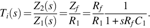
An integrator is a low-pass filter, which is consistent with this transfer function. The integrator rolls off at a frequency of 1/2πRfC1.
Fig. 5.17 shows the Pspice simulation results for an op amp integrator with R1 = 10 kΩ, R2 = 1 kΩ, Rf = 10 kΩ, C1 = 1 nF. The figure shows both the magnitude and phase response. These plots are in the form of a Bode plot with frequency on the x-axis and log voltage output or phase on the y-axis.
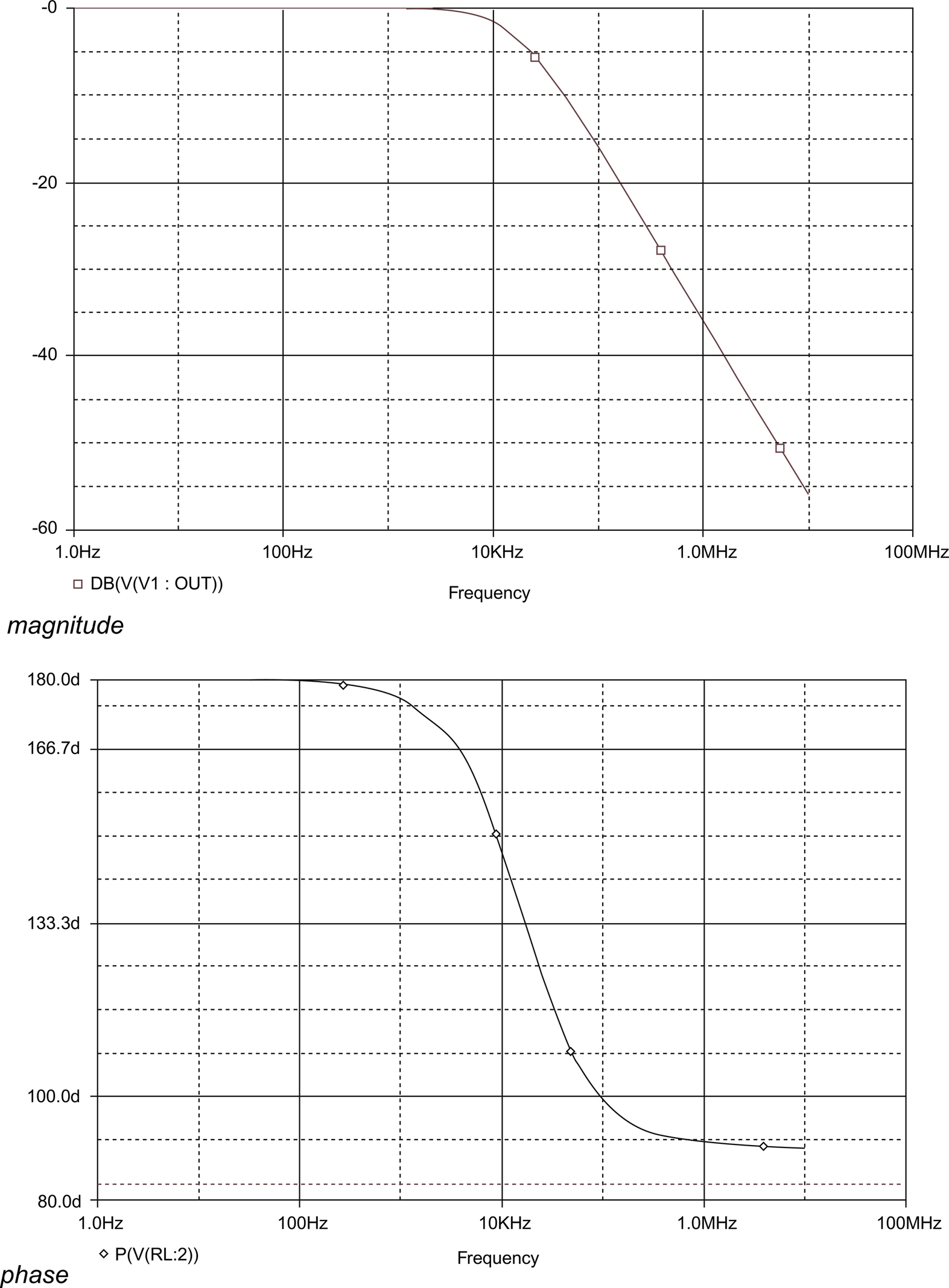
The phase response of a filter can be an important aspect of its operation; we will see a simple example of the importance of phase in Section 5.7. At low frequencies, the integrator introduces a 180° phase shift; at high frequencies, it introduces less of a phase shift. The transition between these two regions is centered on the corner frequency of the filter, 10 kHz in this case.
A differentiator is a high-pass filter. Fig. 5.18 shows a differentiator circuit [41]. The basic differentiation function is provided by C1, R2. Both legs of the filter are built as RC sections to create a band-pass filter. Its transfer function is

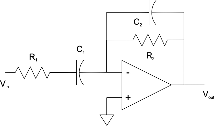
The low-frequency rolloff occurs at 1/2πR2C1. The filter has two high-frequency rolloff points. We can increase the sharpness of the cutoff by choosing the component values such that

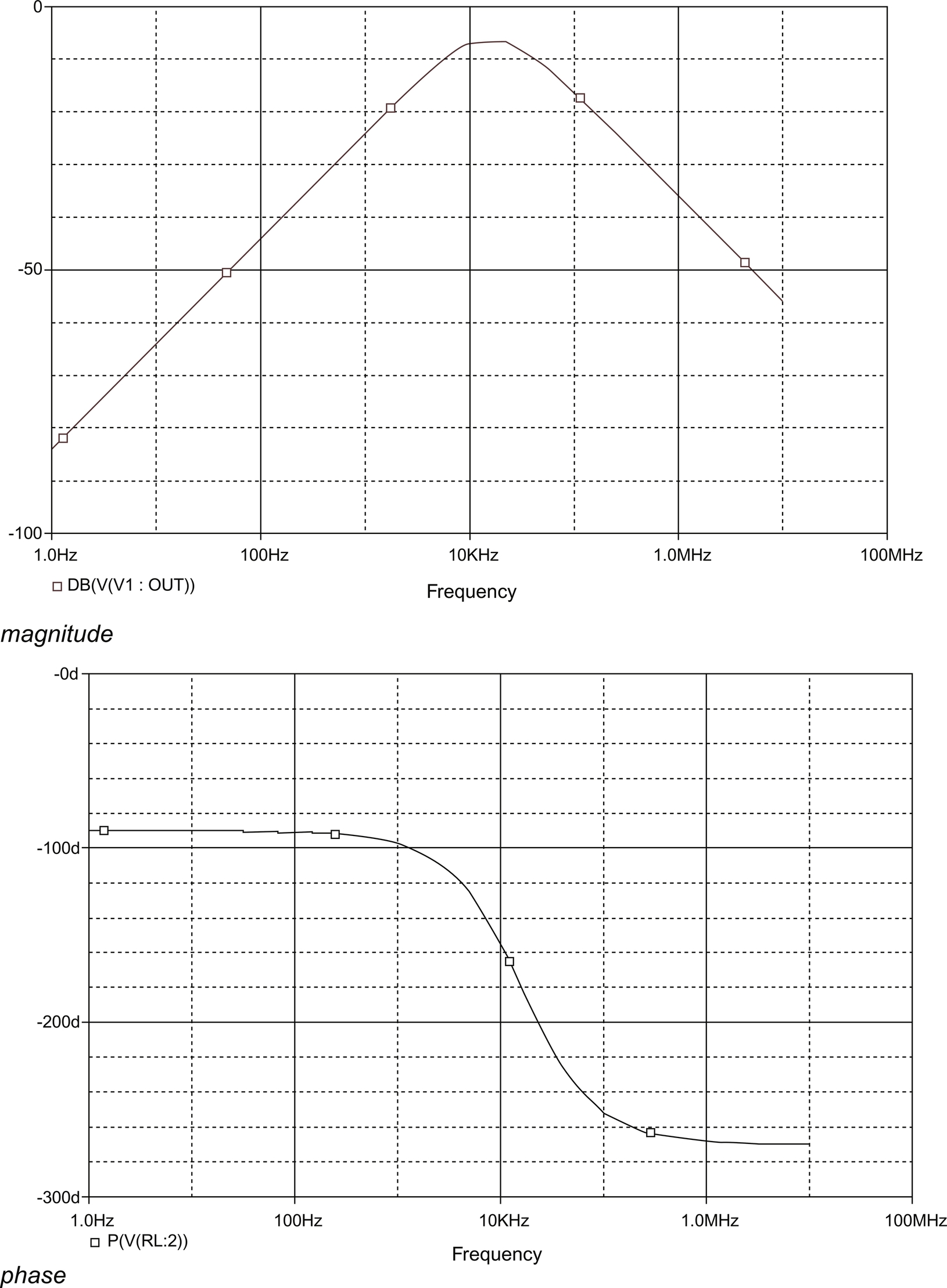
Fig. 5.19 shows the Pspice simulation output of an op amp differentiator with R1 = 10 kΩ, , C1 = 1 nF, Rf = 10 kΩ, C2 = 1 nF. The output magnitude goes up with frequency, indicating that it sees more change on the input, then rolls off thanks to the feedback capacitor. The phase response has a shape similar to that of Fig. 5.17 but with different absolute values.
5.7 Example: Bass Boost Filter
Bass boost filters are commonly used to emphasize bass for audio systems. Fig. 5.20 shows the schematic for a simple bass booster that operates in two phases. The input signal goes directly to the second stage in one fork; in the other fork, it goes to a low-pass filter. As we will see shortly, we should pay attention to the phase of the low-pass filter's output. The second stage is a summing circuit that adds together the two signals.

Fig. 5.21 shows the Pspice schematic for the complete bass boost filter. The first stage is a low-pass filter with a corner frequency of 1/Rf ∙ C1 = 20 Hz. This op amp is configured as a noninverting amplifier so its output is in phase with its input—the output is shifted in phase but is still close in phase to the input. We want the phases of the two signals to be similar so that they do not subtract when combined. We use a summing amplifier as the final stage to combine the bass signal with the input signal; we use a fixed resistor here for simplicity.

Fig. 5.22 shows the frequency response of the bass boost filter. This simulation uses the AC sweep mode of Pspice: the input source V1 is a voltage source whose frequency is swept over a specified range; the output shows the dB voltage levels over that frequency range. The result is similar to a Bode plot but shows measured values rather than asymptotes. In this case, the bottom curve is the response of the first stage and the top curve is the final output. The bass boost output shows the contribution of the low-pass filter.

The second stage uses an inverting topology. The resistor tree at the negative input delivers a voltage to the negative terminal determined by the sum of the signals into the two branches of the tree. If we use equal-valued resistors in the tree and the feedback circuit, the sum is equally weighted. If we use a potentiometer at the branch fed by the low-pass filter, we can vary the amount of bass boost.
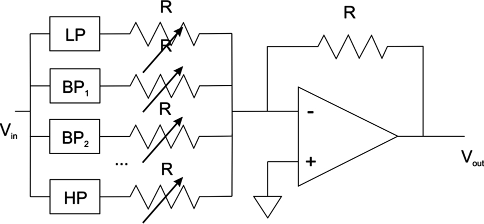
We can generalize the structure of the bass boost to create an audio equalizer as shown in Fig. 5.23. An equalizer divides the audio range into bands and provides adjustable levels in each band. This example uses three bands but more are possible. Each band has its own filter. We choose the passband frequencies for adjacent filters at the same point to provide reasonably flat coverage—the − 3 dB points at the passband edge add together. We use potentiometers in the resistor tree at the final stage to control the level of each stage.
5.8 Advanced Filter Types
If we are willing to move beyond the biquadratic form and allow for a larger number of poles and zeroes, we can create several different types of filters that provide more dramatic response curves. These different types of filters each has its own advantages and disadvantages. We refer to the different filter configurations as approximations because they approximate the characteristics of a perfect brick-wall filter. For all these filters, we can choose the order of the filter: higher order means stronger filter behavior but also more expensive implementation. Each of these approximations is formulated in terms of a low-pass filter. If we want a filter of another type, we can apply transformations from the low-pass form to the desired form.
The Butterworth approximation distributed the zeroes of the transfer function equally around a circle on the s plane. This results in a transfer function whose slope is maximally flat at DC. The transfer function rolls at a rate proportional to the number of zeroes. The result can be a strong drop-off from DC to the edge of the passband.
The Chebyshev approximation uses ripple in the passband to achieve maximal flatness. The ripple means that the filter gain alternates between decreasing and increasing with frequency through the passband. The number of ripples is equal to the order of the filter. This configuration provides higher stopband loss than is possible with the smoother Butterworth filter. The Chebyshev zeroes are distributed along an ellipse.
The elliptic approximation uses a combination of poles and zeroes in the stopband to provide a maximally flat stopband. As a result, the stopband loss is closer to the specified loss, unlike the Chebyshev filter which gives greater than required stopband attenuation. The elliptic filter is widely used due to its efficiency satisfaction of the filter specification.
Although audio applications are generally insensitive to phase, digital signals require careful control of phase characteristics. The Bessel approximation is used to provide a flat passband and good control of phase characteristics in the passband.
5.9 Digital Filters
Digital filters do not suffer from parasitic or temperature variations that affect analog filters. As we will see in Chapter 6, digital waveforms do suffer from sampling limitations; we must also consider numerical effects. We often use a combination of analog and digital filtering.
Digital filters can be designed in either of two forms: finite impulse response (FIR) or infinite impulse response (IIR). IIR filters are smaller but also suffer from more numerical issues. Both are synchronous systems that operate under the control of a clock. We can build digital filters in software or directly in logic; we concentrate here on logic implementations.
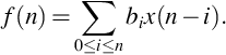
Fig. 5.24 shows the structure of an FIR filter. The z− 1 operators are unit delay operators that are implemented as registers. Coefficients bi are multiplied along some some paths. The products are added together to produce the filter output. The structure can be written as
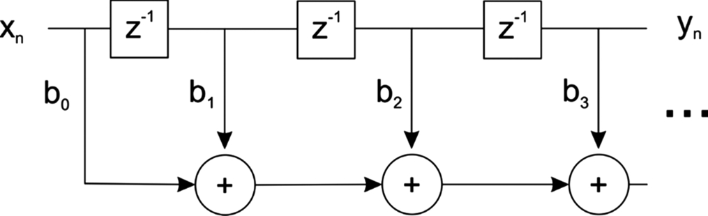
The order of the filter is equal to n. An FIR filter has no feedback. As a result, its impulse response is finite—if we put a unit impulse into the filter's input, the filter's output will return to zero after n cycles. The lack of feedback also means that the maximum value of a signal is limited.
Several different algorithms can be used to design the coefficients of an FIR filter from its specification including the window method and the Parks–McClellan algorithm.
Fig. 5.25 shows one type of structure that can be used for an IIR filter; other types of structures can also be used. The IIR filter includes feedback which results in the potentially time-unbounded response of the filter. IIR filters generally require less hardware than do equivalent filters. The coefficients of an IIR filter are generally found by transformation from an analog transfer function, for example, an elliptical approximation.

Digital filters operate on finite-sized words. We must choose word size to allow for the range of values that can be computed. The dynamic range of the filter depends not only on that of the input signal but also the coefficients in the filter. The dynamic range of the input signal can be represented as
The most extreme values that can be generated in an FIR filter are

IIR filters require more care since feedback means that the signal can grow to unbounded levels.
Digital filters can be built using word-parallel or word-serial arithmetic. Word-serial structures introduce latency since a single word operation takes several clock cycles. But word-serial structures can be built.
Many FPGAs include hardware multipliers in their logic elements. The combination of native multipliers and a large number of registers makes FPGAs well suited to digital filtering.
5.10 Pulse and Timing Circuits
The LM555 timer [19, 66], generally known as the 555 timer, is a popular IC thanks to its versatility. It can generate pulses over as many as seven orders of magnitude of time. It can generate either a single pulse or a pulse train. It operates over a wide range of voltages and is designed to provide stable timing over a large temperature range.
Fig. 5.26 shows a schematic for the 555. The trigger input greater than VCC/3 causes a pulse to be generated: the flip-flop state is set; the flip-flop drives an output stage to provide a large current to the output. When the threshold voltage reaches 2VCC/3, the flip-flop is reset. This causes the discharge transistor to be turned on—it can sink a large current. The flip-flop can also be reset with a negative pulse. A control voltage can be used to adjust the threshold.
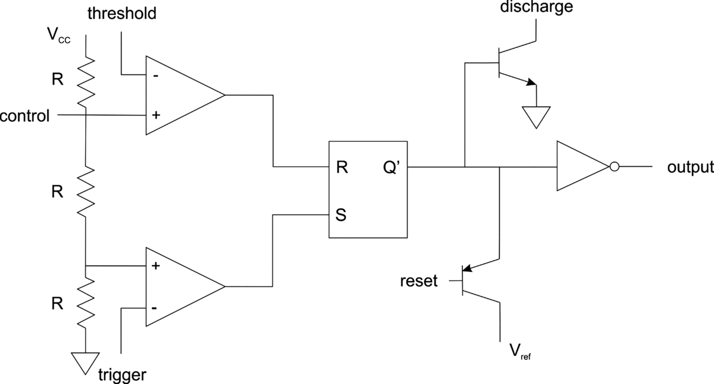
Fig. 5.27 shows a 555 timer configured to operate as a one shot, also known as a monostable multivibrator. A trigger input causes an output pulse of a known length to be generated. One shot is widely used to condition short pulses and ensure that be sure that they satisfy a known duration. The duration of the pulse is determined by the value of capacitor C1. A pulse causes the output to be driven high, providing a current to charge C1. When the output voltage reaches 2VCC/3, it sets off the threshold comparator. As a result, the internal flip-flop is reset, the output drive stops, and the discharge transistor is turned on to discharge C1. The control input is not used here; its value is maintained at C2.

Fig. 5.28 shows the relationship between time delay and the values of C1 and RA. A wide range of time delays can be implemented using various combinations of component values.

5.11 Signal Generators
Fig. 5.29 shows a 555 timer configured as an astable or multistable multivibrator [66]. This circuit generates a stable train of pulses. It does so thanks to feedback—the timing capacitor is connected to the trigger. A trigger input causes C1 to start to charge through RA + RB; when it reaches 2VCC/3, it triggers a discharge through RB, which continues until the voltage reaches VCC/3. Since the trigger is negative, this low voltage causes a trigger that starts another cycle. The period of the pulse is given by the sum of the charge and discharge times:
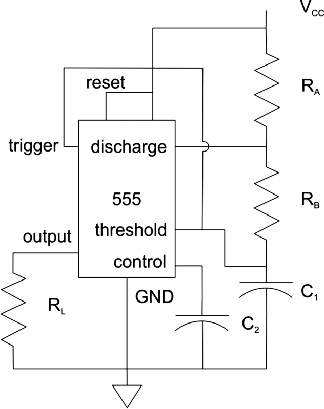
The control input can be used to modify the duty cycle of the pulse. Changing the control voltage modifies the threshold voltage that determines when a pulse is triggered.
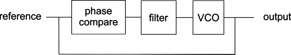
We sometimes want to generate a pulse train at a higher frequency relative to an input pulse train, for example, when we translate a low-frequency reference signal into a high frequency clock. The phase-locked loop (PLL) can be used to generate signals at multiples of an input frequency. As shown in Fig. 5.30, the phase-locked loop is a closed-loop control system which compares the difference in phase between the reference signal and output signal; that error signal is used to adjust the frequency of a voltage controlled oscillator (VCO). PLLs must be carefully designed to provide required accuracies but integrated PLL generators are widely available.
Triangle waves and sawtooth waves have a variety of uses. Triangle waves are sometimes used as substitutes for sine waves as driving waveforms. An accurate triangle wave is easier to generate than a high-quality sine wave. As shown in Fig. 5.31, a triangle waveform has approximately equal upward and downward slopes while a sawtooth has one side of the tooth much steeper than the other. Some authors treat the two terms as synonymous but maintaining a distinction between the two types of waveforms is useful.

We can build a sawtooth or triangle waveform generator based on the astable multivibrator. Feeding the pulse train into an op amp integrator results in a sawtooth waveform whose up and down slopes depend on the duty cycle of the pulse.
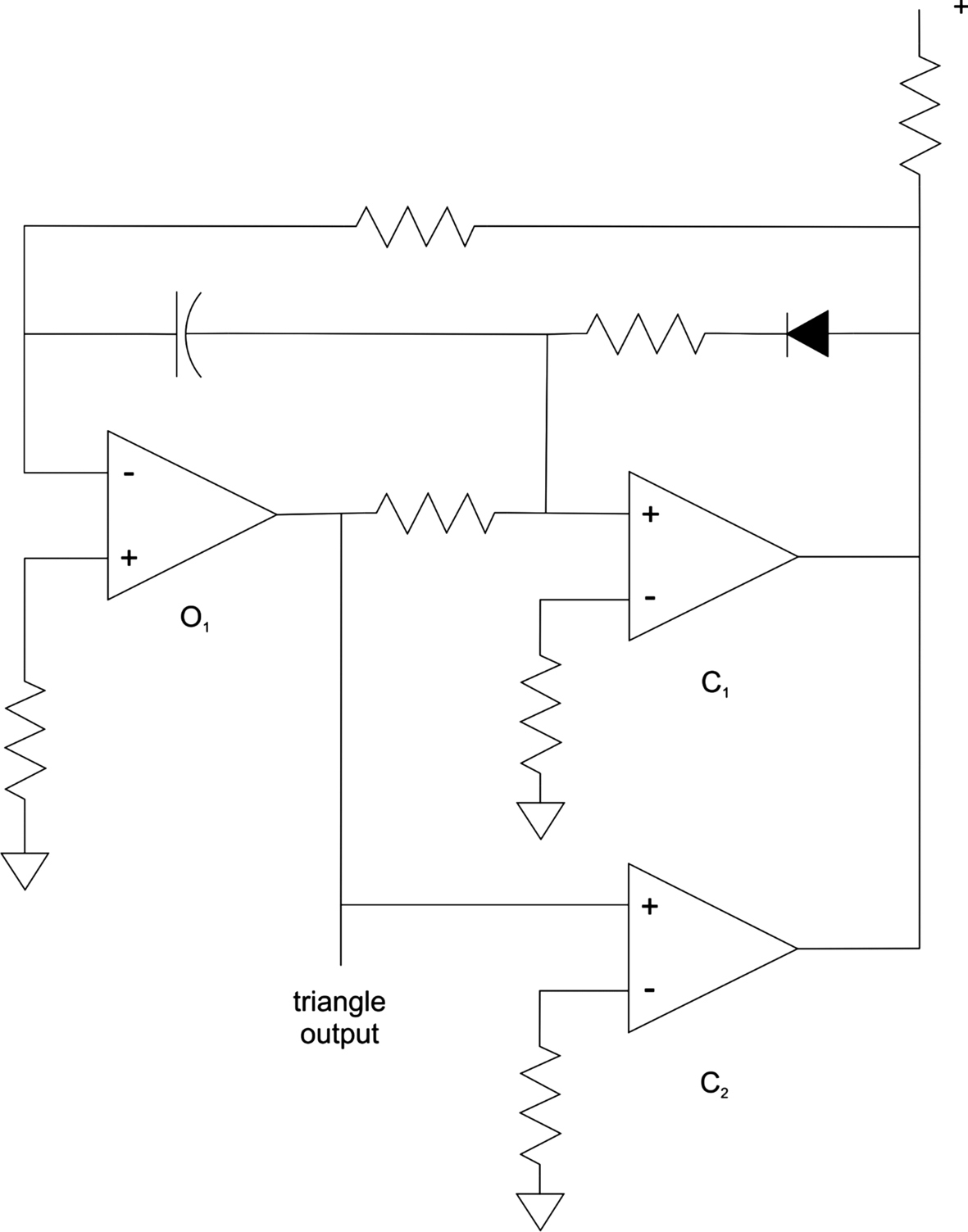
We can also generate a triangle waveform using the circuit of Fig. 5.32 [59]. The op amp O1 is configured as an integrator and generates the triangle waveform. The two comparators C1, C2 determine when O1 switches between positive and negative slope segments: C2 causes the switch from negative to positive slope; C1 causes the transition from positive to negative slope. The diode in the C1 feedback loop allows it to latch its state.
We can use diodes to build circuits that generate piecewise linear approximations of waveforms. Fig. 5.33 shows a waveform and its piecewise linear approximation. Each linear segment has a characteristic slope that we will trace by changing the gain of the output amplifier. The breakpoints are represented by voltages.

Fig. 5.34 shows the waveshaper circuit [63]; additional breakpoints can be added with more diodes and resistors. The input to the circuit is a simpler waveform such as a triangle. The diodes are used to enable and disable resistors on the input leg to the op amp; by changing the input leg resistance, we modulate the gain of the op amp and change the slope of the output. We solve equations for the slopes of the curves and breakpoint values to find the values of the resistors.
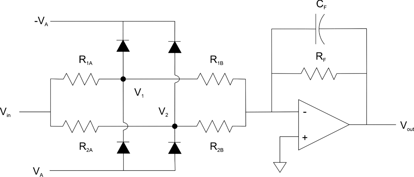
The slopes of the piecewise linear segments are determined by the op amp gain. Since Av = − RF/RD where RD is the resistance of the input leg resistor network, enabling and disabling different resistors in the network changes the slope of the output waveform. The feedback capacitor provides a small amount of smoothing for the waveform.
The breakpoint values are determined by the voltage dividers formed by the AB pairs of resistors. At low values of Vin, both diodes are off and the input leg resistance is
Let the voltage divider ratio D2 = R2B/(R2A + R2B). When V2 = VinD2 = VA − 0.7V, the right-hand control diodes turn on and shorts out R2B, resulting in a change in the input leg resistance to the op amp. Similarly, when V1 = VinD1 = VA − 0.7V, the left-hand control diodes turn on, shorts out R2B, and once again changes the op amp's input leg resistance.
The standard method to build an accurate frequency reference, short of an atomic clock, is a crystal oscillator. Crystals exhibit the piezoelectric effect which trades mechanical stress and electrical oscillation: put a crystal under mechanical stress and it causes an electrical signal through it to oscillate; put an oscillatory signal into the crystal and it produces a small mechanical deformation. Crystals have two important properties that make them excellent frequency references. First, they provide a very accurate frequency that is determined by the properties of the crystal and how it is cut. Second, the crystal's behavior is stable under a broad range of environmental and operating conditions. Crystals also have very high Q.
Fig. 5.35 shows an equivalent circuit for a simple model of a crystal [5]. The crystal operates at a base frequency modeled by C0 while the series RLC stage models harmonic imperfections. (A more accurate model would also include additional RLC stages for higher-order harmonics, which occur at odd multiples.) Overall, the impedance of the crystal falls with increasing frequency. The crystal exhibits two resonant frequencies that are close together: one results in a low reactance while the other results in a high reactance.

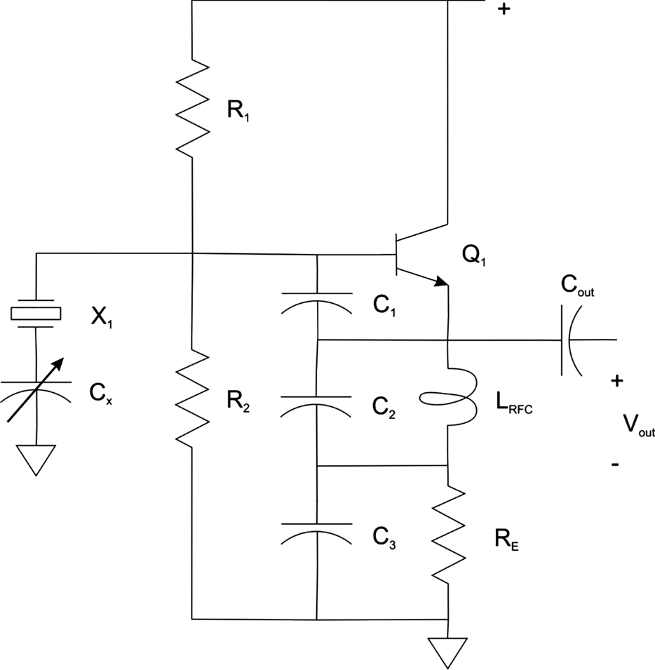
Fig. 5.36 shows a crystal Colpitts oscillator [5]. The crystal provides an oscillatory input. The tank circuit consists of a radio frequency inductor and a pair of capacitors connected in a voltage divider.
5.12 Example: Arbitrary Waveform Generator
A digital block provides a good way to build an arbitrary waveform generator. This device periodically generates samples from a table; changing the table contents changes the output waveform. We will concentrate here on the digital design; the samples can be sent to an analog/digital converter for conversion to an analog waveform.
As shown in Fig. 5.37, the samples are stored in an SRAM. To simplify the design, we use it strictly as a ROM; its contents are initialized by the FPGA configuration. We could add an interface to the waveform generator to allow new sample values to be downloaded while the FPGA is powered on. The sample controller maintains a counter to cycle through the samples in the SRAM. The speed at which it generates the waveform is controlled by the clock input. A separate counter is used to provide a multiplication factor for sample generation. Given a multiplication factor of M, the sample controller waits M clock cycles between samples. The waveform generator module instantiates these two components, wires them together, and wires them to the clock and reset inputs.

5.13 Signal Detectors
A comparator IC [61] is used to generate a discrete signal based on the difference of its two inputs V+, V−. A comparator uses a differential pair at its input, much like an op amp, but its output stage is designed to produce a discrete output, not a linear one. Unfortunately, we use the same schematic symbol for a comparator and an op amp.
We can also use op amps to compare two voltages. We are not in these cases using the linear characteristics of the op amp, but rather saturating its outputs to one or the other power supply rail. While an op amp is not specifically designed to drive logic gates, their voltage levels and current output are more than enough to provide valid signals for many logic families. A comparator provides a good way to make a decision in the analog domain and translate the result to a digital value.
Fig. 5.38 shows an op amp comparator. The V+ input is fed by a voltage divider that provides the reference voltage to which Vin is compared. R3 is a pullup resistor that ensures the output goes to VCC when the output is supposed to be high.

Amplitude modulation (AM) is used in broadcast radio and other forms of communication. As shown in Fig. 5.39, the amplitude of a carrier signal at a higher frequency is modulated using another signal. The peak-to-peak smoothed version of the modulated signal, known as the envelope, traces the modulating signal. AM is used in radio because audio frequencies cannot be efficiently transmitted; the carrier signal allows for propagation at higher frequencies.
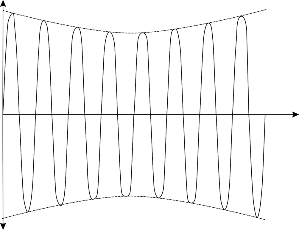
Fig. 5.40 shows an AM detector circuit, also known as an envelope detector. The diode provides the nonlinear element required for detection; the RC filter smooths the waveform. This circuit is very similar to the rectifier circuit we will see in Chapter 7 for AC-DC power conversion.

With the proper selection of time constants, we can use this detector to measure the envelope of other types of waveforms. Envelope values can be used, for example, as level controls. Thresholding the envelope can also provide a signal to initiate some other action.
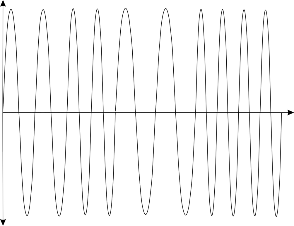
Frequency modulation, shown in Fig. 5.41, modifies the frequency of the carrier rather than its amplitude. FM provides higher signal-noise ratios since physical noise sources tend not to disrupt the frequency modulation effect.
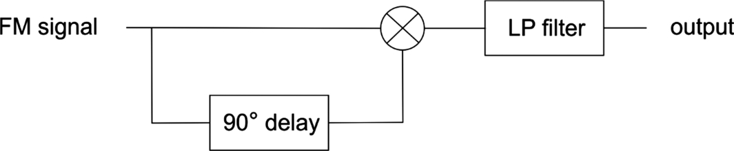
FM detection requires more sophisticated circuits and several different types of detectors have been invented. Fig. 5.42 shows a quadrature detector: it mixes the signal with a version of the signal that is delayed 90 degrees relative to the carrier frequency. The mixer produces several products. A low-pass filter is used to select a version of the baseband signal.
5.14 Example: Headphone Jack Detector
Comparing to a reference voltage allows us to detect events such as plugging in or unplugging a signal. A very common example is detecting when a headset has been plugged into an audio device.
Fig. 5.43 shows a circuit used to detect when external devices are plugged into a headphone port [1]. The V− input is connected to a voltage divider formed by R1, R2 that generates a reference voltage; capacitor C1 shorts out AC signals. The V+ input has its own voltage divider formed by resistors 212 and 214; it also has a shunt capacitor to filter out transients. The R3, R4 voltage divider is used not only to test whether something is plugged into the port, but also with C2 shorting out AC signals. If nothing is plugged into the port, the R3, R4 voltage divider directly determines the V+ voltage.

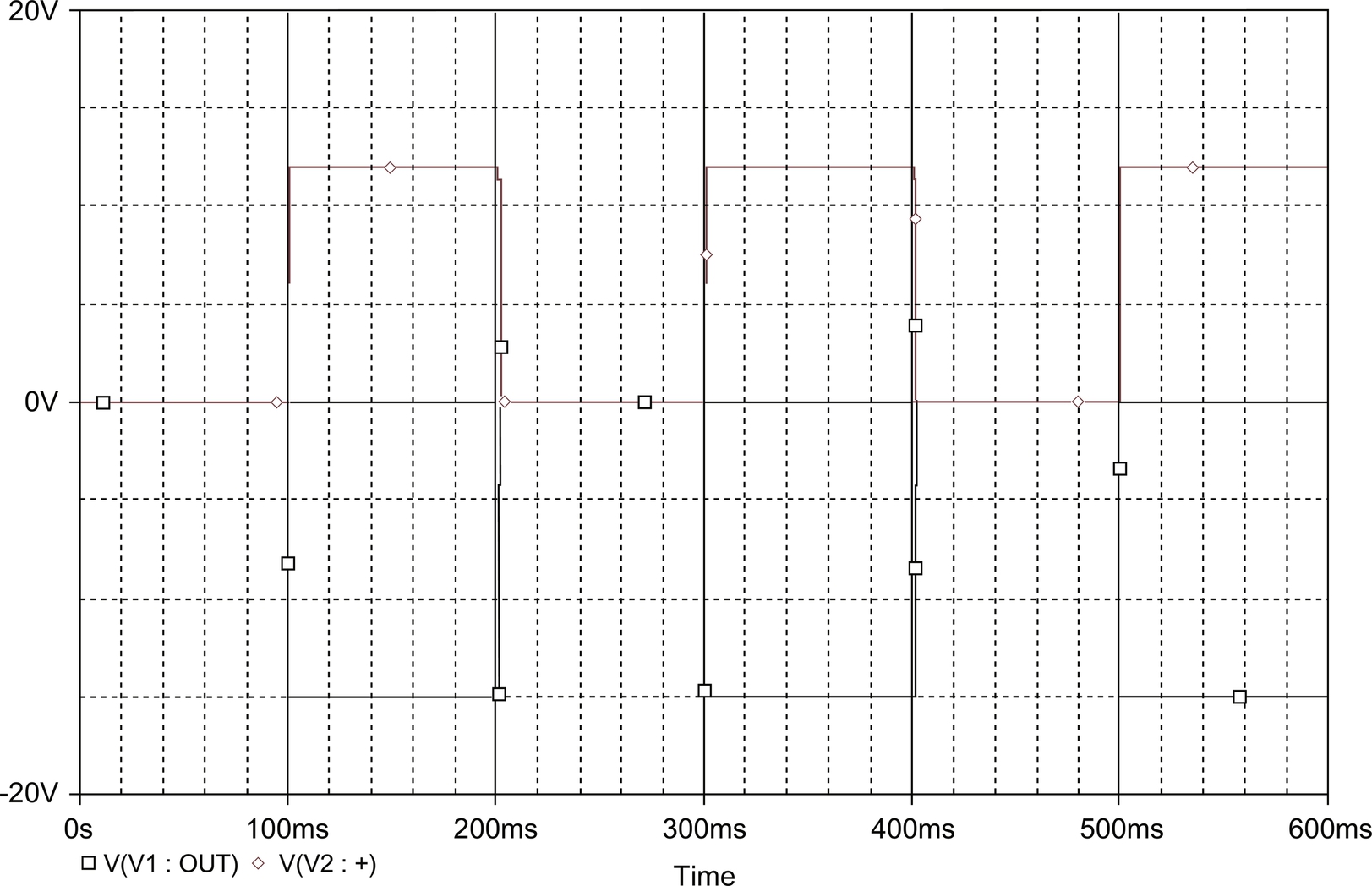
The voltage dividers are used to define a known voltage. The comparator compares that known voltage to the voltage at the jack—if the jack voltage is higher than the reference, nothing is plugged in. We can choose the relative values of the two voltage dividers to ensure that the op amp's output will be high. If we plug a speaker into the port, its low impedance, along with the current-limiting transistor R5, will be in parallel with R4. As a result, the V+ will go down to a low enough value to be below the V− level, causing the op amp's output to switch to the opposite value. The output of the detector can, for example, be connected to one of the CPU's interrupt signals. Detecting a plug event can then signal the driver to perform the required housekeeping operations to respond to the signal.
Fig. 5.44 shows the Pspice schematic for the jack detection circuit. A MOSFET is used to model the connection and disconnection of the 8Ω speaker; a voltage pulse circuit is used to drive the MOSFET's gate and turn the transistor on and off. Fig. 5.45 shows the behavior of the circuit—when the MOSFET is on and the speaker resistance is connected to the input, the op amp output goes negative, indicating a connection.

We can build several detectors with different thresholds to detect which of several different devices has been plugged in, assuming that the different devices have sufficiently different impedances that we can reliably distinguish between them.
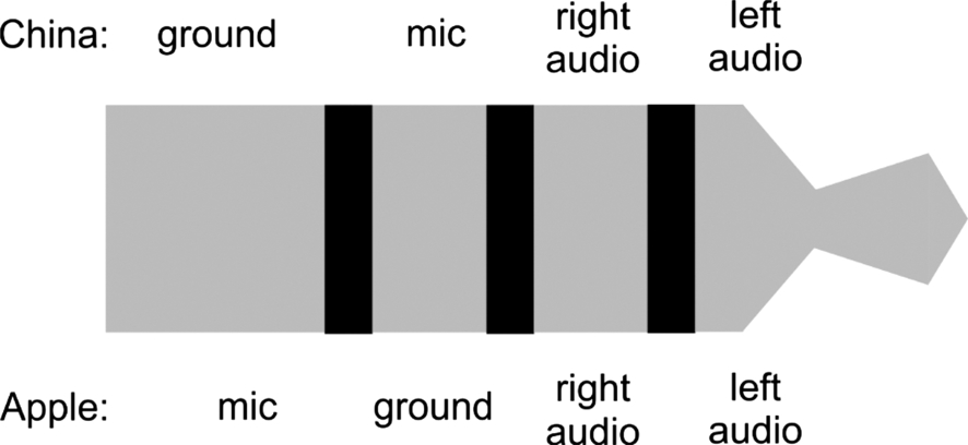
An example 3.5 mm headphone jack is shown in Fig. 5.46. The jack is divided into four different conducting areas separated by insulators. This arrangement, known as a TRRS jack for tip/ring/ring/sleeve, allows for three different signals and a ground/signal return. The ability to detect multiple devices is particularly useful with modern headsets that include both microphone and speakers. First, we need to be able to distinguish between a headset that has only stereo speakers versus one that includes a microphone as well as speakers. Second, two different configurations of the four-conductor speakers-plus-microphone arrangement exist. As shown in Fig. 5.47, headphones differ as to where they put the signal return relative to the other signals. One configuration is known as the China headset configuration while the other is known as the Apple configuration. Neither configuration provides a functional advantage; the two configurations exist simply because no industry standard was developed. Since both types of headsets are in common usage, audio devices must first detect a jack insertion, then test the terminals to see which configuration is in use, then connect their internal circuits to the proper sections of the jack. The combination of connections can be sequenced using either a digital finite-state machine or a software controller.

The TPA6166A2 [65] is an audio amplifier chip that also detects when accessories are connected and their TRRS configuration. When a jack is detected as having been insertion, the chip runs an algorithm to determine its TRRS configuration; it requires two consecutive configuration operations to determine the same type for it to consider the result reliable.
Further Reading
Lancaster's Active Filter Cookbook [33] provides a thorough introduction to active filters. Jung [32] discusses a wide variety of precision op amp circuits. Daryanani [17] describes the design of op amp filters in detail. McClellan et al. [39] describe digital filters in detail.
Questions
- Q5.1 Draw a filter specification diagram for a low-pass filter with ωp = 4k, ωs = 5k, Amax = 3 dB, Amin = 50 dB.
- Q5.2 Draw a filter specification diagram for a high-pass filter with ωp = 10 k, ωs = 8 k, Amax = 1 dB, Amin = 60 dB.
- Q5.3 Draw a filter specification diagram for a band-pass filter with [ω1, ω2] = [1k, 4k], [ω3, ω4] = [500, 5k], Amax = 3 dB, Amin = 50 dB.
- Q5.4 Draw a filter specification diagram for a band-reject filter [ω1, ω2] = [2k, 10k], [ω3, ω4] = [1.5k, 10k], Amax = 1 dB, Amin = 50 dB.
- Q5.5 Draw a Bode plot for a low-pass filter with a gain of 20 dB at ω = 0 and one pole at ω = 2kr/s.
- Q5.6 Draw a Bode plot for a high-pass filter with a pole at ω = 0, gain of zero at ω = 0, and one pole at ω = 2kr/s.
- Q5.7 A series RLC circuit has R = 1 kΩ, L = 1 μH, C = 1 μF.
- (a) What is its resonant frequency ωr?
- (b) What is its Q?
- Q5.8 Give a biquadratic transfer function for a low-pass filter with ωp = 4k, Qp = 25.
- Q5.9 Give a biquadratic transfer function for a high-pass filter with ωp = 10k, Qp = 50.
- Q5.10 Find feedback component values for an active RC low-pass filter with R1 = Rf = 1 kΩ, fp = 5 kHz.