
Power
Abstract
The quality of power delivered to circuits can profoundly influence the proper operation of those circuits. Power supplies must deliver a required output voltage and current; voltage ripple is another important metric. An understanding of power supply design helps us to choose the proper power supply. AC-to-DC supplies convert alternating current to direct current. Power converters transform DC to DC. Batteries have several important characteristics that influence system design. Many embedded computers use power management hardware and software to manage their power consumption. A simple linear regulated power supply is used as an example.
Keywords
Power supply; Power supply voltage; Maximum output current; Output voltage ripple; AC-to-DC power supply; Power converter; Batteries; Power management
7.1 Introduction
The power supply is the unheralded hero of circuit design. The importance of a high-quality power supply becomes apparent only when we try to use a bad power supply. We sometimes build our own power supply. As with most types of circuits, a solid understanding of their design helps us to choose the proper power supply even when we use a prebuilt supply.
The next section considers the specifications for a power supply. Section 7.3 analyzes the design of AC-to-DC power supplies. Section 7.4 looks at the design of DC-DC power converters. Section 7.5 discusses batteries as power supplies. Section 7.6 designs a simple AC-to-DC power supply using discrete components. Section 7.7 considers thermal characteristics of electronics and heat dissipation. Fig. 7.8 discusses power management.
7.2 Power Supply Specifications
The most basic specification of a DC power supply is its output voltage and maximum output current. The maximum output current is typically specified relative to a load impedance. Many power supplies provide several different output voltages all derived from a common core.
Output voltage ripple is a very important specification for digital and particularly for analog circuits. Ripple does not have to be periodic; in this case, it refers to any variation in the output voltage. While digital circuits tend to be relatively insensitive to power supply voltage, large amounts of ripple may cause errors. Analog circuits are particularly sensitive to power supply ripple. Since output voltages are produced relative to the power supply, variations in the power supply result in variations in those outputs.
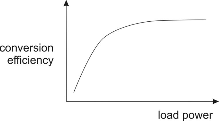
Conversion efficiency measures the ratio of power delivered to the load to the total power consumed by the power supply. As shown in Fig. 7.1, efficiency varies with the power delivered to the load. Most power supplies are less efficient at low loads—the overhead power consumption of the supply generally does not scale well with load power.
Heat dissipation is an important metric that may determine the case used for the system or whether it needs some form of active cooling such as a fan. Power supplies do not always directly specify their heat output. However, we do know that for a given power output, more efficient power supplies will produce less heat.
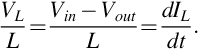
The ground voltage is often used as a reference voltage throughout the circuit. The term ground is not chosen arbitrarily. A true earthed ground is directly connected to the Earth through a low-resistance connection. The voltage of the Earth is very difficult to change—Gauss’s Law tells us that any charge sent to the earthed ground will be equally distributed across the surface of the Earth. Since a great deal of charge is required to noticeably change the voltage of the Earth, it provides a very good reference voltage.
Power supplies for mixed-signal systems generally provide a separate analog ground that is distinct from the digital ground. Digital signals can generate large swings that produce variations from the nominal ground voltage. Since analog signals are particularly sensitive to power supply noise, we want to isolate the analog circuits from noise created by the digital circuits.
Safety is a critical requirement for power supplies. Shocks from AC utility lines can be fatal. Improper design of power supplies can lead to fires. Even low voltages can damage other devices. We must carefully design power supplies to minimize their risk of dangerous operation and failure.
Batteries require some specialized specifications; we will defer their discussion to Section 7.5.
7.3 AC-to-DC Power Supplies
As shown in Fig. 7.2, an AC-to-DC power supply operates in four stages. The transformer stage transforms AC from one voltage to another. The rectifier stage converts the AC voltage from voltages both above and below ground to a waveform that is always nonnegative. The filter stage filters the rectified waveform into a DC waveform with ripple. The regulator stage reduces the ripple of the waveform.

A transformer is a pair of coupled conductors. The transformer windings are generally made around a metal core to increase their efficiency. The two windings are known as the primary winding at the input and the secondary winding at the output. The secondary voltage is determined by the ratio of primary to secondary windings:

We can rectify the AC waveform using either half-wave or full-wave rectification. Fig. 7.3 shows examples of each: The half-wave rectified waveform includes only half of each sinusoid; the full-wave rectified version flips the lower half of each sinusoid.

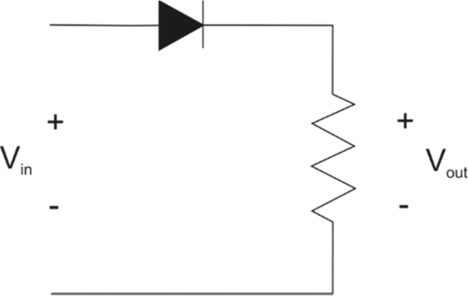
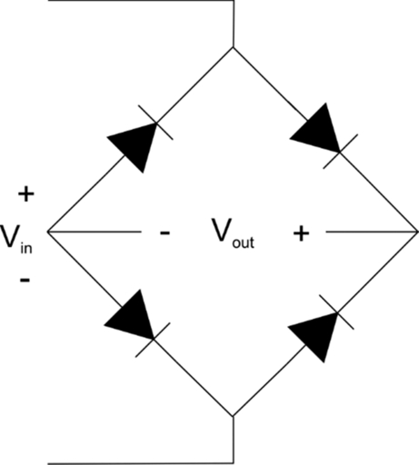
As shown in Fig. 7.4, a diode is sufficient for half-wave rectification. The lower half of the waveform is cut off by the diode when it is in its reverse bias region. In the forward bias region, it conducts the AC waveform. Full-wave rectification makes use of a diode bridge shown in Fig. 7.5. The output of the rectifier is taken from its two interior terminals. On the positive side of the input waveform, one pair of diodes conducts; on the negative side, the other diode pair conducts. This clever configuration flips the negative half of the waveform to create the full-wave rectified waveform. A full-wave rectifier is much more efficient than the half-wave version because the half-wave rectifier throws away half of the waveform.
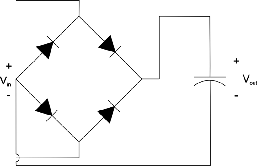
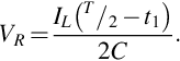
One or more capacitors are used to filter the rectified waveform as shown in Fig. 7.6. The capacitor acts as a low-pass filter on the rectified waveform. The larger the capacitor, the lower the ripple. After the rectified waveform reaches its maximum value, the filter capacitor is discharged at a constant rate by the load current as shown in Fig. 7.7.

We can find the ripple at the filter output for a given load current IL. As shown in Fig. 7.8, the voltage moves between VH and VL with 2VR = VH − VL. The ripple waveform has a period equal to half of the sinusoid period:
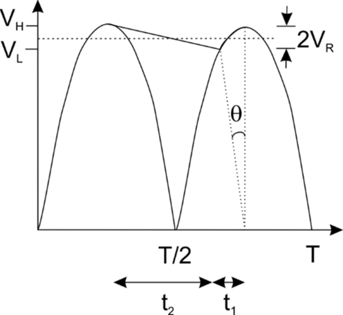
A simple estimate for the ripple voltage is given by the capacitor law:


A more accurate estimate comes from finding the intercept between the current discharge ramp and the sinusoid:

Since

we find
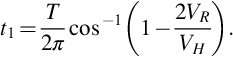
We can use this value for t1 to find an improved value for VR:
Power supply filter capacitors must be rated to withstand high voltages. Electrolytic capacitors are generally used for the filter stage. We generally connect bleeder resistors across the filter capacitors to bleed off current when the power supply is off; the bleeder resistors have high resistance values to avoid draining too much current during operation.
We can use either linear or switching regulators to reduce the ripple produced at the final output. A simple linear regulator is shown in Fig. 7.9. This circuit uses a Darlington pair as a series regulation transistor Q1.

A Zener diode is often used to create the reference voltage source. A Zener diode is designed to be operated in reverse bias; unlike standard diodes, they do not break down due to reverse bias current. The reverse bias voltage can be controlled by manufacturing, which allows Zener diodes to be manufactured in a wide range of stock reference voltages.
A voltage divider is used to measure the output voltage that is compared to the reference voltage. The voltage divider resistors are chosen based on the Zener diode reference voltage chosen. The Zener diode controls the regulation transistor. When the output is below the reference voltage, the regulation transistor supplies current proportional to the difference between the output and reference voltage. When the output is above the reference voltage, the regulation transistor is off, allowing the power supply output to droop as it supplies current to the load.
We can also build switching regulators that perform on-off control of the output voltage. A comparator is used to compare the output voltage to a reference value. The regulation transistor is used in switching mode rather than linear mode. Switching regulators provide higher efficiency than do linear regulators. But switching regulators must be carefully designed to avoid oscillation.
Many power supplies make use of integrated regulators, which provide good power quality as well as protection and other features. The LM340 [40] is a common three-terminal power regulator. It can be used as a fixed regulator by connecting capacitors to its input and output. The output voltage can be adjusted by replacing the output capacitor with a voltage divider. It can be used as a current regulator by using a resistor to turn the output current into a voltage for regulation. The LTC 3780 [34] combines buck and boost converters to provide DC-DC conversion at voltages both below and above the input voltage.
7.4 Power Converters
Power converters are used to convert one DC voltage level to another; the term is also used for DC-to-AC converters. While a power supply may be designed to supply several different voltage levels, we often make use of voltage converters to supply a specialized voltage for part of the circuit rather than find a power supply that provides all the required voltages.
Three common types of switching power converters are the buck converter (which converts a higher voltage to a lower one) and the boost converter (which converts a lower voltage into a higher one) and the flyback converter (which can be designed to supply multiple voltages). All these converters are nonlinear regulators; they are very efficient but also require careful design to avoid feedback-induced instability.
Fig. 7.10 shows a buck converter circuit [36]. We close the switch during the on portion of the duty cycle ton, 0 ≤ D = ton/(ton + toff) ≤ 1. When the switch is closed, the inductor is energized with current. The charging current through the inductor increases with time as given by the inductor law:
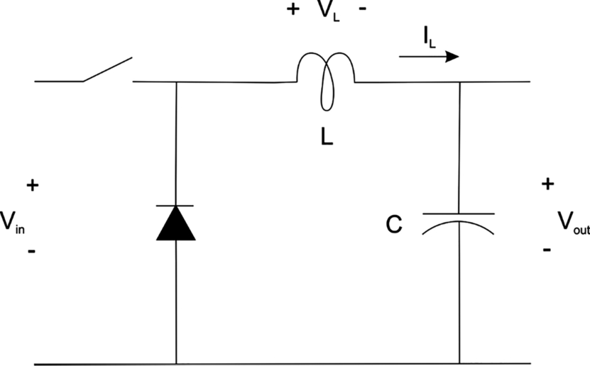
The current waveform is a ramp whose maximum value is
When the switch is turned off, the inductor current discharges into the capacitor. The diode provides current continuity. The current decreases at a rate
The inductor current goes to zero when the voltage across the inductor reaches zero. The net change in voltage across the inductor over the duty cycle is zero. While the slopes of the charge and discharge waveforms may differ, we know that the charge and discharge phases balance:
Rewriting,

The analysis of the boost converter, shown in Fig. 7.11, is similar, but in that case Vin ton = Vout toff.

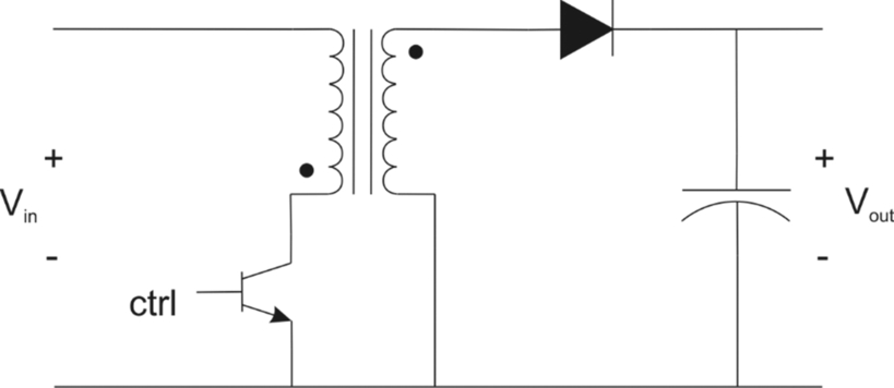
As shown in Fig. 7.12, a flyback regulator makes use of a transformer. (The term flyback transformer comes from the cathode ray tubes used in early television, where it was used to generate the sawtooth waveform used to return the cathode ray across the screen.) The winding ratio of the transformer determines the relationship between the input and output voltage. The dots on the transformer indicate that its windings provide opposite polarities. The ctrl input is a pulse width modulated signal that switches the transformer primary on and off. When the primary is on, the diode prevents secondary current from charging the capacitor. When the primary is off, the energy stored in the secondary is used to charge the output capacitor. We can provide several different power supplies using a transformer with multiple secondary windings, each with its own winding ratio and connected to its own diode and capacitor.
7.5 Batteries
An electrochemical cell can provide electrical energy to a circuit. A battery is a group of electrically connected cells, but we often use the term battery to describe any electrochemical storage device.
The most basic characteristic of a battery is its capacity, measured in Amp-hours. The battery's C rate is equal in value to its capacity; designers sometimes scale charge and discharge currents by C. The energy density of a battery describes its capacity per unit weight.
Fig. 7.13 shows a typical battery discharge curve [53] which we can use to understand some other battery specifications. As the battery is used to supply power, its voltage drops slowly. The midpoint voltage VMP is at the middle of the battery's operating region and is used to characterize the battery. The slope of the discharge region varies considerably for different types of batteries. As the battery nears its discharge limits, its voltage drops much more quickly. The end-of-discharge voltage VEOD, also known as the end-of-life voltage, marks the point at which the battery ends its useful discharge.

A battery has an equivalent series resistance that limits its peak current. The self-discharge rate of the battery determines the length of time over which it will hold a charge.
The details of battery specifications vary widely with the battery chemistry. A number of different chemistries have been developed over a period of several centuries. Alkaline batteries, for example, are commonly used in devices that make use of replaceable batteries. The most common chemistries for rechargeable batteries in electronics are nickel-cadmium (NiCD), nickel-metal hydride (NiMH), and lithium ion (LiIon).
When discharging a battery, we can monitor voltage to determine when the battery is about to reach its end-of-discharge voltage. Many battery management ICs provide signals that indicate when the battery has reached the dropout voltage at which the battery is no longer useful without recharging.
Recharge schemes can be classified into three categories [75]:
- • Trickle charging provides a low discharge current.
- • Constant voltage charging operates at a constant battery voltage.
- • Constant current charging provides a constant charge current.
The exact type of recharge cycle required for a battery depends on its chemistry. A LiIon charging cycle starts with a precharge trickle charging phase, followed by constant current fast charging, and finally a constant voltage taper charge [2]. Fast charging—charging at high C values—can damage a battery by generating excessive heat. Fast chargers must sense when the battery is fully charged and switch to a slow charging mode to avoid damage to the battery; the end of the charging cycle is often determined by a combination of voltage and temperature [54]. Fast charging rates can also cause the battery to charge less fully as the chemical processes for charging vary with charge rate.
7.6 Example: Linear Regulated Power Supply
An AC-to-DC power supply designed to regulate 120 V introduces notable safety risks. We can safely explore power supply circuits using Pspice. We will build up a linear regulated supply in stages.
Fig. 7.14 shows the schematic of a simple circuit with a transformer and full-wave rectifier. The transformer is specified with a 1:10 ratio of primary to secondary windings to reduce the 120 V input to 12 V. The transformer secondary is connected to the full-wave rectifier. Fig. 7.15 shows the rectified output across a 1 kΩ load resistor.

Fig. 7.16 shows the Pspice schematic for an unregulated supply, which adds an output capacitor in parallel with the load resistor. The value of the capacitor was chosen for this example to give a noticeable ripple. Fig. 7.17 shows the unregulated output.


Fig. 7.18 shows the regulated power supply. This circuit uses a Zener diode as the voltage reference; its breakdown voltage is 5.1 V. The resistor feeding the Zener diode is chosen to give a 20 mA current. The R1, R3 voltage divider is designed to divide the desired output voltage of 10 V to a level equal to the Zener reference voltage; their series resistance is chosen to be a high value to minimize their current draw on the power supply output. Fig. 7.19 shows that the regulated output is very smooth without the need for an additional capacitor across the load. The plot also shows the op amp output that controls the regulator transistor.


7.7 Thermal Characteristics and Heat Dissipation
We need to control the temperature of electronics for several reasons: circuit characteristics may vary significantly over wide temperature ranges, high temperatures cause components to fail more rapidly, and very high temperatures may pose a fire hazard.
A critical thermal parameter for semiconductors is maximum junction temperature Tj, max. Junction temperature refers to the semiconductor junctions; if these junctions go above a specified temperature, either the device quickly destroys itself or its thermal protection circuits shut down the device. A value of Tj, max = 150°C is common for digital VLSI while power semiconductors may see ratings of Tj, max = 85°C. We maintain all the semiconductors below Tj, max using a combination of low-power design to reduce the heat generated and heat dissipation to efficiently remove heat from the devices.
The TO-220 heat sink, shown in Fig. 7.20 , is designed to be mechanically compatible with the TO-220 package, used by a number of electronic components. The component can be bolted onto the heat sink. The thermal connection to the heat sink allows for improved heat dissipation.

Fan vs. fanless design is an important design decision in many systems. Fans greatly improve cooling but introduce acoustic noise. If fans are used to reduce component temperatures, the enclosure must be properly designed to allow for airflow into and out of the cooling region.
We can analyze the temperature of components using a thermal resistance model [74]. In this model, thermal resistance is analogous to electrical resistance, heat is analogous to current, and temperature is analogous to voltage. The ambient temperature—the temperature of the surroundings—can be treated as analogous to electrical ground if the circuit cannot generate enough heat to substantially increase the ambient temperature.
Many components are rated with a thermal resistance by manufacturers. When a component is connected to a heat sink, the system has a lower thermal resistance. We can also use various thermal compounds between the component and the heat sink to reduce the thermal resistance from the core device to the ambient.
Fig. 7.21 shows the circuit model for a simple thermal dissipation problem: the component dissipates power P and has a thermal resistance θ to the ambient. The ambient is shown as a ground but it has a nonzero reference value TA. The temperature difference T from the component temperature TC to the ambient TA is

Our goal for semiconductor cooling is to ensure that TC < Tj, max.
When a device is not mounted on a heat sink, we use the junction-ambient thermal resistance θJA. This value is given by the manufacturer in many cases.1 In the case of the LM340 voltage regulator in a TO-220 package, θJA = 54°C/W [40]. At a power dissipation of 5 W and an ambient temperature of 25°C, the LM340’s junction temperature is 295°C, clearly too high.
When we connect the device to a heat sink, we just compute the thermal resistance of the assembly [3]:
where θJC is the junction-to-case thermal resistance, θCS is the case-to-heat sink thermal resistance determined by the thermal paste applied between the device and heat sink, and θSA is the heat sink-to-ambient thermal resistance. In the case of the LM340 and TO-220 package, θJC = 4°C/W. We can use a typical value of θCS = 0.1°C/W. The TO-220 heat sink data sheet quotes θSA = 12°C/W for no airflow [30]. This gives θJA = 16.1°C/W and TJ = 105.5°C, well within the safe zone for this device.
Active cooling using fans makes a big difference in junction temperatures. If we provide an airflow of 5m/s, θSA = 4°C/W and TJ = 65.5°C.
Heat causes electrical and electronic components to age and fail faster. Aging mechanisms can be traced back to chemical and physical processes. The Arrhenius equation describes the relationship between the rate of a physical mechanism and temperature [52]; it has been shown to apply to a wide variety of processes related to aging. The equation has the form
where r is the rate of the process, A is the Arrhenius prefactor for a given physical mechanism, and Ea is the activation energy. The exponential dependence of rate on temperature means that rate doubles for a 10°C temperature rise.
The aging of electrolytic capacitors is an example of the application of the Arrhenius equation [49]. The lifetime of an electrolytic capacitor as a function of operating and ambient temperature is
where L0 is the capacitor's specified lifetime, Tmax is the maximum temperature, and Ta is the ambient temperature.
Aluminum electrolytic capacitor has higher losses than do some types of capacitors. As a result, ripple currents generate heat. The ripple current at an arbitrary frequency is referenced to a standard frequency by the formula

where Ix is the actual ripple frequency and k is a coefficient specified for the part. The increase in temperature at the surface of the capacitor caused by ripple current is

where I is the ripple current, R is the equivalent series resistance of the capacitor, and S is the capacitor's surface area, and
The temperature increase at the capacitor's core is

where I0 is the rated ripple current of the capacitor.
7.8 Power Management
Most computer systems make use of power management implemented through a combination of hardware and software. The system may turn off units that are not currently in use; it may also run some units at lower voltages and clock speeds to conserve power.
An interface may need to accept power management signals and shut off some circuits. Power-up is often the trickiest part of power management. Any state that was held in dynamic devices must be restored from a nonvolatile memory; in some cases it can be recomputed by running the system. Analog circuits may display transients as the circuits power up or down—the click of an audio system during power up/down or when headphones are connected or disconnected are a classic example of annoying transients.
Further Reading
Sauvageau [50] describes testing procedures for USB power adapters and the design characteristics that affect both power performance and safety. Battery Reference Book [15] describes a broad range of battery chemistries.
Questions


- (a) Which diodes are on in region a?
- (b) Which diodes are on in region b?
- Q7.2 A 12 V, 60 Hz power supply includes an output-stage capacitor of 50 μF. What is the maximum allowable load current to keep the ripple within 2%?
- Q7.3 Draw the waveforms for the operation of a buck converter, including the switch, VC, and IL.
- Q7.4 Draw the waveforms for the operation of a boost converter, including the switch, VC, and IL.
- Q7.5 An IC dissipates 10 W and has a maximum junction temperature Tj, max = 150°C. The ambient temperature is 20°C.
If the device is exposed directly to the ambient without a heat sink, what is the required thermal resistance of the package to keep the device's junction temperature below the specified maximum?
What must the package's thermal resistance if it is used with a heat sink with thermal resistance θSA = 12°C/W and θCS = 0.1°C/W?