
Interface Design
Abstract
An embedded system interface is itself a part of a larger embedded system and the interface design process is one part of the overall embedded system design. Interface design selects two important boundaries: between CPU software and digital interface logic; and between the digital and analog sides of the interface. Use cases for embedded systems help us understand interface requirements. Interface design methodologies provide a structured approach to the design of interfaces that meet performance, power, and cost goals. Design examples include a clap detector and motor controller.
Keywords
Interface design methodology; Computing platform; Device driver; Hardware/software boundary; Analog/digital boundary
8.1 Introduction
We now have a toolbox of techniques, both analog and digital, for interface design. It is time to put these techniques together to design complete interfaces. The interface is itself a part of a larger embedded system and the interface design process is one part of the overall embedded system design.
The design of an embedded system interface can be seen as the placement of two boundaries:
- • The boundary between the software on the CPU and the interface's digital hardware.
- • The boundary between the interface's digital hardware and its analog hardware.
Section 8.2 develops characteristics of common use cases for embedded devices. Section 8.3 looks at requirements on interfaces. Section 8.4 introduces the architecture of an embedded system interface. Section 8.5 considers how to choose a good computing platform. Fig. 8.6 discusses circuit construction technologies. Section 8.7 considers closed-loop control systems. Section 8.8 examines the hardware/software boundary. Section 8.9 develops a simple driver. Section 8.10 looks at the digital/analog boundary. Section 8.11 puts together these concepts as part of the interface design methodology. We then develop two examples: a clap detector in Section 8.12 and a simple motor controller in Section 8.13.
8.2 Embedded System Use Cases
Understanding the characteristics of use cases for embedded systems helps us to identify the important characteristics of their interfaces.
We can infer some basic requirements on the processor and interfaces based on characteristics of the application:
- • CPU performance is a key driver of software development; the class of CPU required to meet performance requirements also constraints the available microcontroller or system-on-chip platforms and their associated interfaces.
- • Sample rate is related to the software load but also to the performance requirements on the interfaces.
- • Network bandwidth requirements to the outside world may constrain the interconnection bandwidth available within the embedded platform.
Table 8.1 estimates these requirements for several common embedded applications: audio-rate signal processing, in the range of several kilohertz, could be applied to applications other than audio; closed-loop control uses a microcontroller to provide commands to a machine to perform in a specified manner; event processing generates data when a specified change in the environment is registered.

8.3 Interface Specifications
We can identify two types of specifications on interfaces: requirements on the interface characteristics and properties of the design process.
Given that interfaces process signals, we are certainly interested in the requirements on that signal processing as determined by the application. Signal processing requirements may relate to both time and resolution.
The data rate or sample rate limits the frequency characteristics of our signal. The latency of processing is often critical; analog/digital and hardware/software design choices may be determined by how long we have to process a signal.
The precision and dynamic range of a signal reflect the required resolution of the signal. Interface design needs to preserve enough dynamic range of the signal to allow the required processing to be completed.
Power consumption is a key parameter for many designs. Battery-operated devices should be designed to maximize battery life. High power consumption may also lead to excessive heat dissipation.
The design process must consider both the manufacturing cost and the design time of the interface. Both are important and the two may be at odds with each other. The cost of the interface depends on the components selected as well as the costs of fabricating the associated circuit board. Design time is itself a cost; design time may also delay deployment of the product. Interfaces that are simpler to design may increase manufacturing cost; they could also increase the development cost of the system software. Conversely, a more sophisticated design that requires greater design effort may lower manufacturing costs.
8.4 Interface Architecture
Fig. 8.1 shows an architecture template that describes a wide range of interfaces. The bus connects to data and status registers that provide the software interface to the application. A mode FSM controls the operation of the interface. Digital and analog subsystems perform processing on plant signals from the physical world. User controls provide users with means to control the interface separate from the CPU.
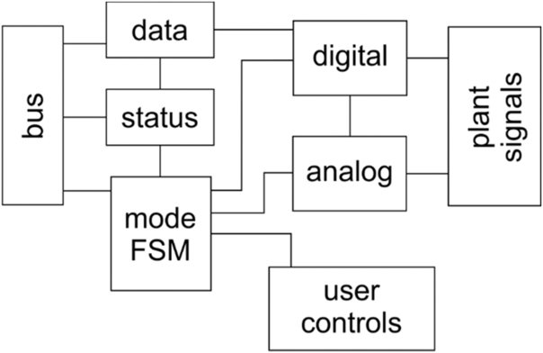
The interface registers provide the only visible state shared by the microcontroller and the interface device. Any software control of the interface must be done by manipulating the registers. We can typically divide interface registers into mode and data categories, with mode registers controlling operation while data registers provide the values. Some registers may be read-only while others will be read/write.
The interface operation can be viewed as a finite-state machine. The mode FSM may be an explicit state machine implemented as logic and registers; it may also be implicit in the operation of the interface circuits. The interface goes into modes based on its own activity; the microcontroller checks status, manipulates data, and may change the mode register to cause the interface FSM to change state. A very simple interface FSM is shown in Fig. 8.2. The idle state may occur when the device has completed an operation. By changing the mode register, the microcontroller can signal the interface to move to the ready state and perform another operation.

8.5 Choosing the Right Platform
The interface designer doesn’t always have the ability to choose the computing platform on the other side of the interface. We sometimes have to live with the characteristics of a microcontroller or SoC which was chosen for reasons beyond the characteristics of the embedded interface. No matter who chooses the platform, its characteristics shape the design of the interface.
The hardware platform includes several related components:
- • The processor or, in the case of high-performance systems, several processors. Some of the processors may provide only limited programmability, as is the case for many video accelerators.
- • The set of I/O devices provided by the platform.
- • The bus interface.
- • The software development environment.
The software platform includes:
- • A hardware abstraction layer (HAL), board support package (BSP), or basic input/output system (BIOS).
- • Device drivers.
- • An executive or operating system.
If our platform is built from several chips, we may be able to separate these choices to some degree. However, modern platforms often take the form of a single-chip microcontroller or system-on-chip. In these cases, the platform selection process must balance these potentially competing factors.
CPU performance determines what part of the system functionality can be put in software. CPU performance may enforce absolute limits—it may not run fast enough to perform, for example, digital filtering operations. But performance can also be evaluated relative to the rest of the application. A system with a large software load may leave few cycles for interface-oriented operations, no matter how much performance it provides.
We should keep in mind that CPU performance depends on a number of factors. There is no one best choice for a CPU instruction set or microarchitecture. A CPU that works well for one workload may perform poorly for another workload. CPU performance should be evaluated not on the basis of generic workloads but by using workloads that reflect the characteristics of the target application.
CPU utilization is a key metric for real-time embedded systems. Utilization is defined as the fractional amount of CPU execution time of a set of tasks Ci over a given interval T:
We often express utilization as a percentage. Utilization may vary over the course of operation as the workload varies. We are generally interested in worst-case utilization over any interval. We cannot exceed 100% utilization that would require more CPU time than is available. The maximum available utilization of the CPU depends in part on the real-time scheduling algorithm used.
Interrupt latency is a critical design parameter for high-speed I/O processing. CPUs themselves can introduce dozens of clock cycles of processing time into the interrupt; the interrupt driver itself adds more overhead as it saves and restores registers.
The arithmetic precision required for I/O processing is affected by the choice of CPU. We can always combine smaller words to perform wider integer operations or to perform floating-point operations in software, but software-implemented extended arithmetic requires additional CPU time.
The platform comes with some set of I/O devices and interfaces. Any devices or interfaces that are required for the project but not part of the basic platform must be designed into the interface. Relatively few modern chips directly expose the CPU bus. General-purpose I/O (GPIO) pins are a common form of interface; these pins are easy to use but provide only modest speeds. Some chips may provide an external DRAM interface that could also be used for other devices; such interfaces are much faster but also much more challenging design targets.
Bus performance of the I/O system. The bus throughput is proportional to the product of bus width and bus clock cycle time. CPU busses come at many different design points providing different cost/performance trade-offs. While high-performance busses provide faster I/O, they also require more complex interface designs for the peripherals attached to them.
The software development environment (SDE) will influence the overall development process. Not only do the features of the SDE determine how code will be developed, but its debugging capabilities will influence how much of the interface debugging can be accomplished from the software side vs. using test instruments such as logic analyzers. An integrated development environment (IDE) provides a graphical user interface for the tools in the software development environment.
On the software side of the platform, we can identify several basic components, some of which may be supplied with the CPU or board while others may be acquired separately. Most systems use low-level routines to provide basic functions: boot, real time clock, etc. This low-level software can be called any of several names: hardware abstraction layer, board support package, or BIOS (a term from the IBM Personal Computer).
Fig. 8.3 shows a layer diagram for the software organization of the embedded system. The hardware platform is at the bottom layer. The hardware abstraction layer provides basic software functions. Drivers may work through HAL functions or directly on the software. The executive or operating system controls the operations of tasks that perform the application-level functions.
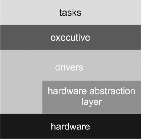
While the hardware abstraction layer may provide some drivers for standard functions such as USB, the designer may need to provide other drivers. A driver for the interface must be designed. The details of driver design depend on the type of operating system or executive used. We will discuss driver design in more detail in Sections 8.8 and 8.9.
The term executive is an early term for a simple operating system. A real-time operating system is designed specifically to provide real-time responsiveness for both I/O and process execution. Linux is widely used in embedded devices; not all versions of Linux are designed to provide highly responsive performance for I/O and real-time operation.
We will refer to the top-level software units as tasks, each of which is a single thread of execution that is guaranteed to terminate in a finite amount of time. A task may run more than once, either sporadically or periodically. A complete application may be composed of several tasks.
A system with a small number of tasks may use interrupts to manage task execution. Periodic tasks can be controlled by a timer. Sporadic events can also be used to trigger interrupts. Given that microprocessors have a limited number of interrupt lines, this approach does not scale to large number of tasks.
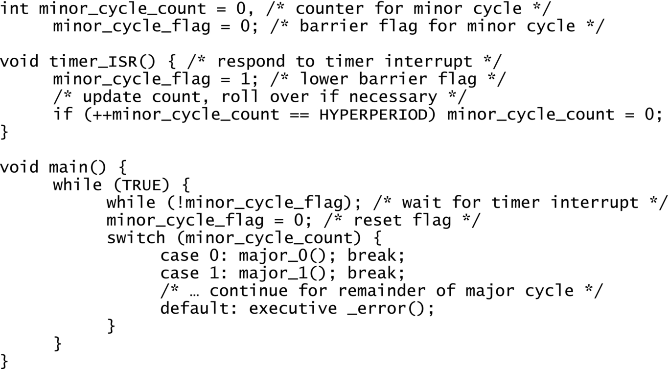
A cyclic executive [6] can be used to provide predictable timing behavior for periodic tasks in a simple real-time system. If each task has its own period, the pattern of task activations is equal in length to the least-common multiple—also known as the hyperperiod—of the task periods. The hyperperiod defines a major cycle for the operation of the executive. The schedule is the order of execution of the tasks in the major cycle. The minor cycle must be at least as small as the shortest period of any task. The executive is called or enabled once per minor cycle by an interrupt. It keeps track of its progress through the major cycle to control what tasks are performed.
Fig. 8.4 gives pseudo-code for a simple cyclic executive. The executive is contained inside a while (TRUE) loop. The timer interrupt causes its handler timer_ISR() to set a flag minor_cycle_flag that is visible by the main routine and to update a counter minor_cycle_count that gives the value of the current minor cycle. The executive proceeds only when the flag is set, indicating that another minor cycle has been completed; it resets the flag to prepare for the next minor cycle. It then uses a counter to determine which part of the major cycle should be executed next. A task is implemented as a function. Each task must terminate in a finite amount of time. Once the function returns, the executive returns to wait for the next minor cycle to finish.
A real-time operating system (RTOS) uses preemptive multitasking. A timer is used to call the operating system once per time quantum. At each time quantum, the current state of the executing task is saved; the RTOS determines what thread should run next; it then restores the state of the selected task. RTOSs typically support a priority-driven scheduling policy—the highest-priority ready task runs.
8.6 Construction Technologies
Some electronics construction technologies are designed for one-off prototyping; others were created to manufacture multiple units.
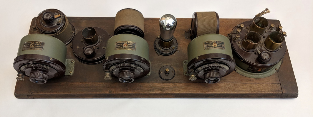
Fig. 8.5 shows a radio manufactured by the Atwater Kent Manufacturing Company in Philadelphia in the early 1920s. Thanks to the opening of KDKA in Pittsburgh and the birth of commercial radio broadcasting, radios changed in a matter of months from esoteric experimental equipment to a centerpiece for homes of the well-to-do. Atwater Kent made several radio models built on boards such as this one. These radios came to be known as breadboards after the boards used to cut bread in kitchens of the day. The company advertised the breadboard construction as a means to display the high quality of their components; it is equally likely that the style was dictated by the breathtaking speed with which the radio market expanded. Breadboard later came to mean a prototype circuit built on a board with point-to-point hand wiring even though the original term referred to an expensive manufactured device.
The prototyping module of Fig. 1.16 allows easy construction of certain classes of circuits, namely, dual inline packages and components with extended leads. Protoboards cannot connect to surface mount devices without adapters. Protoboards are prone to large parasitic values due both to loose wiring and the connections themselves.
Early printed circuit board manufacturing relied on through-hole connections between a component and the board. As shown in Fig. 8.6, a hole was drilled through the PCB and plated with copper. The component lead was inserted in the hole, which was then filled with solder. Modern PCBs primarily use surface mount connections that solder the lead to a copper pad on the surface of the board. Some chips provide solder bump connections in an array across the bottom of the chip.
8.7 Control and Closed-Loop Systems
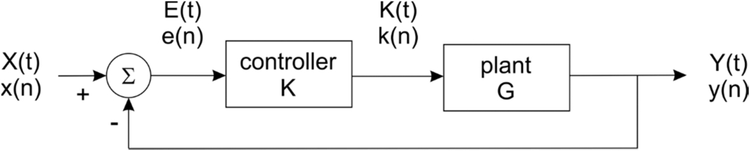
Feedback control is a fundamental engineering technique for controlling all sorts of physical plants: mechanical, electrical, chemical. The feedback controller generates an error signal as the difference between the actual output of the plant and the desired output. The control law defines the controller response which commands the plant to change its state closer to produce an output closer to the desired value. A block diagram for a feedback control system is shown in Fig. 8.7. The command is X(t) in the continuous time case or x(n) in the discrete time case; the error signal is E(t) or e(n); the controller output is K(t) or k(n); the system response is Y(t) or y(n).
We typically specify the control system based on its step response, which represents its response to an instantaneous change in the command. Three characteristics are used to describe the step response:
- • Rise time is the time from the command to the first time at which the response reaches a specified value, typically 90% of the asymptotic response.
- • Overshoot is the maximum value of the response.
- • Settling time is the time at which the response is bounded within some amount of the asymptotic response, with ± 1% a typical value.
A classical approach models both the plant and controller as linear systems. A typical second-order transfer function for a physical plant is

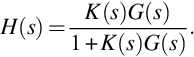
If the controller response is K(s), the closed-loop transfer function is
A proportional-integral-derivative (PID) control law [22] provides a blend of desirable characteristics and is widely used. As the name implies, this control law includes proportional, integral, and derivative terms, each with its own weight. The proportional component provides the basic response to a command input. The integral component ensures that the controller has zero asymptotic error. The derivative component can be tuned to provide fast response to new commands.
Here is the continuous version of a PID control law:
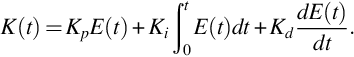
The controller gains Kp, Ki, Kd determine the relative weight given to each component of the control law. The continuous form can be translated to a discrete form:
A modified form differentiates on the control output y rather than the error signal e to avoid a sharp change in the command producing a large derivative term in the control law:
A PID controller is a second-order system:

Its response can take the form of the sum of two exponentials or of a damped sinusoid.
The response of the closed-loop system depends on the plant. For example, consider a first-order plant:

This plant has an exponential response which only asymptotically approaches a final value. When we wrap a PID controller around the plant, the system response becomes

The PID-controlled system has a second-order response which, with proper tuning of the controller gains, can provide a much more responsive system.
In theory, we should know the parameters of the plant transfer function, from which we can determine the controller gains based on the rise and settling times. In practice, we do not always know the plant parameters. In that case, we can experiment with the system to empirically determine the controller gains.
Complex control systems may change their response depending on some condition: user input, changes to the load presented, etc. Hybrid control specifies modes as states that can specify parameters for the controller. Hybrid control design checks that the system response at mode changes meets characteristics such as smoothness.
We need to choose a sample rate for a digital controller. We want the control sample rate to be considerably higher than the highest frequency pole of the control transfer function.
8.8 The Hardware/Software Boundary
The partition between software running on the CPU and interface hardware is the basic decision in interface design. We can expand on our requirements to identify several factors that influence the decision.
Algorithmic complexity. Some algorithms may be hard to implement as analog or digital circuits due to their size or the nature of the operations they perform.
Flexibility. Flexibility comes in several forms. A software routine may be changed after installation of the system. The software may also provide parameters that adjust its operation without changing the code itself. Updates are definitely easier for software than for hardware interfaces. The more parameters for a given function, the more expensive and difficult is the application of those parameters to a hardware implementation.
CPU utilization. An interface can be used to offload some processing from the CPU. High data rates are particularly taxing for software. The cost of a faster CPU must be balanced against the cost of a more sophisticated hardware interface.
Sample rate. CPUs have some basic limits on the rate at which they can process data. Interrupt handling, RTOS overhead, and software performance all limit the speed with which the CPU can perform a computation. An interface can be used to recognize events or to downsample the signals.
Numerical precision and dynamic range. The range between minimum and maximum values on a signal determines both the number of bits required to represent the signal as well as whether that representation is fixed point or floating point. While floating-point units can be built in hardware, such designs are relatively complex. Number representations with larger bit widths increase the size of hardware data paths. In contrast, software number representations may take up more memory but CPU mechanisms exist for several different number representations of varying accuracy.
Latency. Software processing adds latency for interrupt processing and RTOS mechanisms; individual operations may require multiple instructions. Digital interfaces may provide low latency and analog interfaces can be highly responsive.
Many devices will make use of the microcontroller's interrupt interface. The interrupt system allows devices to change the flow of execution in the CPU to an interrupt handler, also known as the interrupt service routine (ISR). Operations in the ISR are performed at the hardware priority level defined by the interrupt—the operating system has no control over those priorities. Hardware interrupts will block other software tasks, including the operating system. As a result, the real-time properties of the system may be violated. The ISR should perform the minimum operations required to service the interrupt; other tasks can be performed in a software task that is under control of the operating system.
As shown in Fig. 8.8, several different software objects are involved in the processing flow of data as it moves from input to output. Interrupt service routines handle the input and output tasks themselves. A software task performs processing. The data flowing into the task goes through one buffer while another buffer handles the flow of data out of the task. Fig. 8.9 shows a UML sequence diagram for the flow of data.


Fig. 8.10 shows a UML state diagram for a driver. Upon entry, the driver typically checks the status of the device to understand what type of service needs to be performed. It may manipulate data, either reading or writing. It then updates the status of the device, for example, to enable its next operation.

8.9 Example: A Simple Driver
We can better understand driver design through a simple character string output interface. While the device itself is of limited practical use, it illustrates basic concepts in drivers without unnecessary complexity. The device is used to output a string of characters, one character at a time.
Fig. 8.11 shows a block diagram for the character interface. The device includes three registers, two one-bit and one eight-bit. The character task writes a character into the char register, then sets ready to 1. The external system sets ack to 1 when it has processed the character. The ack register's output is connected directly to the interrupt logic while ready and char are connected to address logic that maps them into the CPU memory space.
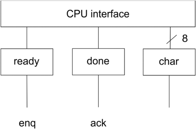
Fig. 8.12 shows the state transition diagram for the mode FSM. The device is normally at idle. When activated by ready, it starts to output the current character. It enters the done state when it receives an acknowledgment. When the task resets the done bit, the interface returns to the idle state. This design is an example of an implicit mode FSM. The interface states are defined by combinations of the status bits; state transitions are caused in this case entirely by external inputs with no additional logic. Table 8.2 presents the mapping of status bits to state names; the code 01 is not used.
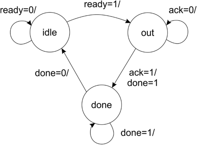
Table 8.2
| State | Code (Ready, Done) |
|---|---|
| idle | 00 |
| out | 10 |
| done | 11 |
This design could be extended to use DMA—the DMA controller would interact directly with the hardware to output the character string. The device state machine may need to be adjusted to be compatible with the DMA protocol. Given that DMA imposes regular timing on the character stream, the other side of the interface may drop some characters.
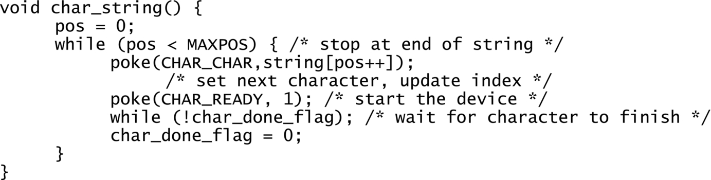
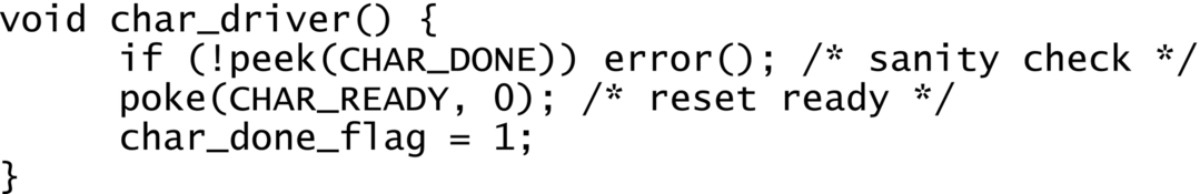
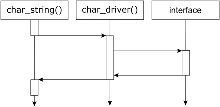
Figs. 8.13 and 8.14 show the character output task and the interface driver, respectively. Fig. 8.15 gives a UML sequence diagram for an output sequence. The task starts a character output by loading the character and setting ready. When the interface receives an ack signal, it raises an interrupt that activates the driver. The driver, in turn, sets char_done_flag to tell the task that the character output is complete.
8.10 The Analog/Digital Boundary
The analog/digital boundary within the interface determines some important characteristics of the interface. Of course, some signals present themselves as analog. However, we often have some choice as to how much processing to perform on the signals in analog form before converting them to digital form.
Signal characteristics. Some signals may be electrically unsuitable for digital logic. Either very small or very large voltages or currents may require conditioning before being handed off to digital logic.
Dynamic range. Processing on a signal may affect its dynamic range.
Temperature sensitivity. Analog circuits are more sensitive to temperature. Component values vary with temperature, resulting in varying circuit characteristics. While analog circuits can be designed to be resistant to temperature variations, digital logic is much more tolerant of temperature variation.
Power consumption. Analog circuits often consume less power to perform a given function than is the case for an equivalent digital logic circuit.
Cost. Some important operations can be performed by very simple analog circuits with a very small number of components. The equivalent digital design may be more expensive.
Latency. The small number of components in an analog circuit often translates to very low latency.
8.11 Interface Design Methodologies
Interface design is one phase of embedded system design. As with any subsystem, we want to separate its detailed design from the rest of the system to the extent possible. But we need to inform the interface design process from the system design: requirements, specification, architecture, and testing.
System requirements and specification include requirements on the signals that will be processed by the interface:
- • Input and output signals.
- • Analog vs. digital values.
- • For analog signals, signal levels and dynamic range.
- • For digital values, logic levels and timing parameters.
Requirements and specification also capture the processing to be performed on those signals:
- • Sample rate.
- • Algorithm.
- • Latency.
The requirements phase also captures the economic factors of design effort and manufacturing cost.
Based on these requirements, the architecture phase sets the software/hardware boundary. This design partitioning process determines what part of the processing will be performed in the CPU versus the interface. This hardware/software boundary is determined in part by technical factors such as sample rate and algorithmic complexity. These factors define a design space which describes the set of feasible designs. Economic factors further constrain the feasible design space.
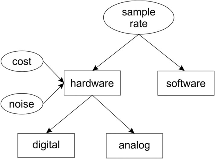
Fig. 8.16 illustrates a decision process for design partitioning. The sample rate for the signal is a key factor in determining what can be done using software on the CPU versus what needs to be done in the interface hardware. Once we have decided what part of the system will reside in hardware, component cost and noise are two important factors that help to determine what functions should be built with digital logic or analog circuits.
Component selection is a critical part of the design process. While some components can be selected later, the selection of major components is part of the architecture phase—the characteristics of some analog and digital components will shape the design of the rest of the interface. Components are selected from catalogs, usually online but occasionally on paper. A catalog may come from a manufacturer and describe the range of components they make. A catalog may also come from a supplier who carries the products of several manufacturers. Search tools are a valuable aid in narrowing down the set of possible components. Many Web sites allow you to enter one or more specifications that are used to narrow the search. Typically entering a few parameters narrows the set of components down to a handful. If a given search results in no results, you need to rethink those parameters and find a set value that is inhabited by a suitable component. Schematic capture tools also provide databases of components and their parameters; these databases allow you to experiment with components before you order.
At this point, design on the interface can proceed relatively independently. Some aspects of the design may be performed relatively independently of the processor platform. Analog design can proceed using a combination of simulators and breadboard circuits. Digital computation units can be designed using standard HDL techniques. However, design of the processor interface may require a prototype. Manufacturers do not often provide HDL models for the CPU bus interface. While a model can be constructed as part of the design process, running the interface against a working bus helps to build confidence in the design.
Interface testing introduces several complexities beyond software testing. First, as we just saw, we may not have an executable or simulatable model of the CPU bus interface. The only way to test the bus interface may be to plug it into the system; this step will also require software scaffolding. Second, analog test signals cannot be captured as data files, as can digital test sequences. Documentation should carefully describe the analog test setup: what signals are generated, the equipment used to generate those signals, and the tests performed on the analog circuits to verify their behavior.
8.12 Example: Clap Detector
A clap detector is a good example of filtering and detection. We can design the clap detector with any of several different hardware/software partitions. We can build a clap detector entirely using analog circuits. However, a purely analog detector would be hard to adjust for clap detection parameters. We may want to adjust level based on the audio environment. The transition and duration may need to be adjusted depending on the amount of echo.
As shown in Fig. 8.17, a clap produces an audio signal in the classic form of a damped exponential. The clap's large damping results in its sharp sound. This waveform suggests a detector architecture that allows us to substantially reduce the CPU's sampling rate. We are not concerned with all the details of the audio signal—the envelope of the clap is sufficient. We can use an envelope detector similar to those we saw in Section 5.13 to rectify and filter the waveform. A low-pass op amp filter can provide a signal to the ADC that is substantially smoother than the original audio filter. We can use a software correlator to compare the input waveform to an exponential model to detect the waveform.
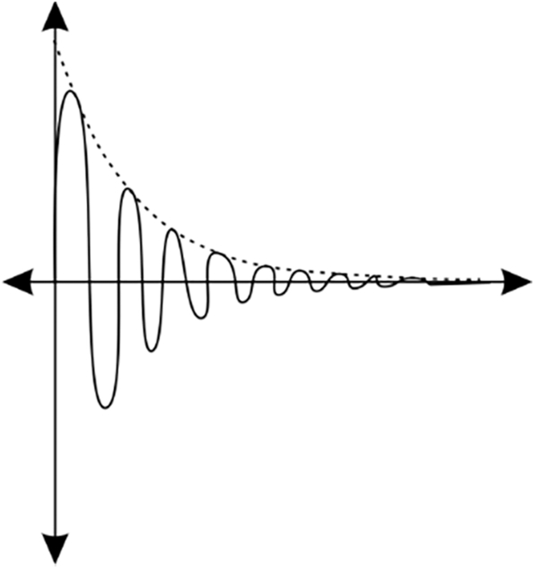
Fig. 8.18 shows the block diagram of the clap detector: envelope detection rectifies and filters the input signal; the ADC generates samples; the detector compares the sampled waveform to a model of the clap exponential. The low-pass filter allows us to operate the analog/digital converter at a lower sample rate than would be required for full audio intelligibility. Reducing the sample rate reduces both the CPU utilization and the sizes of buffers required for the condition operations.

8.13 Example: Motor Controller
Motor control circuits add capabilities and greater precision. We can use feedback to control the speed of the motor—rather than just providing a given amount of power and assuming that it runs at the desired rate, we can measure the speed of the motor and adjust its drive to maintain the speed we want. We can go one step further to build a motor that stops at a commanded position and can be turned to a new position at will.
DC motors come in any of several different designs:
- • A brushed DC motor is the old-fashioned style of motor with commutator brushes that provide alternating connections to the motor windings to keep the motor spinning.
- • A brushless DC motor does not have commutator brushes. Instead, it uses a controller to switch the connections to the motor windings.
- • A servo motor is designed to stop at various positions.
- • A stepper motor has more poles than does a servo motor, providing finer control.
The torque produced by a motor is proportional to its current [10]:
The movement of the motor coils induces a back electromotive force or back EMF that counters the voltage applied to the motor. The back EMF Ve depends on the rotation speed or angular velocity of the motor shaft:
A motor has several specifications, some of which are independent of the control. The operating voltage, maximum current, and maximum rotating speed of the motor are all characteristics that depend on the motor design and are independent of the control we apply to it. The motor characteristics need to be matched to the requirements of the mechanism that the motor will drive.
Selecting a motor is a simple example of the use of online catalogs. A variety of sites allow users to first select DC motors as a category, then specify several search filters: speed, torque, voltage, etc. Our example design will use a motor [43] that operates at 0.23 W at 6 V; at its maximum efficiency point it spins at 2089 RPM.
As shown in Fig. 8.19, we use pulse-width modulation to vary the speed of a motor; we can apply this technique to both brushed and brushless motors. If we applied the power supply voltage continuously, the motor would run at some maximum speed. As we reduce the duty cycle D of the power supply, the motor coasts during the off interval. The result is an average speed which depends linearly on the power supply duty cycle. We can reverse the rotational direction of the motor by reversing the polarity of the power supply relative to the motor's terminals.
The duty cycle resolution is the minimum allowable change to the duty cycle. This resolution determines the precision with which we can adjust the motor speed.
The PWM function is often implemented as a hardware block. Performing the PWM function entirely in software would require a responsive CPU to keep up with time ticks. As shown in Fig. 8.20, a PWM unit consists of a timer and a comparator. The timer counts clock pulses; its period determines the PWM period. A separate register holds a compare value that determines when the PWM output switches from high to low. Since the timer period in real time is the product of the timer clock period and the counting range of the timer, we can adjust the resolution of the PWM unit by choosing the proper combination of timer clock period and timer bit width. Pulse-width modulation can be implemented with a combination of hardware and software: two timers keep track of the PWM period and compare period; software is responsible for switching the PWM output value based on the states of the two timers.

Two characteristics are directly related to the design of the motor controller. Motor speed accuracy depends in part on the control algorithm but also depends on the accuracy of the sensing system used to measure the shaft RPM. We want the shaft rotation speed to be slow relative to the accuracy of the timer used to measure shaft speed; if the shaft rotates at a rate similar to the timer, small variations in shaft speed may result in large measurement errors. The response time measures the time between a command for a new speed and the time at which the motor achieves that speed within some specified accuracy. We can model response time as a step response and use classical control theory methods to design the controller from the response time specification.
The H bridge is widely used to control motors and to allow the power supply to be supplied to the motor in either polarity. The logical organization of the H bridge is shown in Fig. 8.21. It is a relative of the full-wave diode bridge used to rectify AC signals. The voltage across the middle of the H depends on the control signal values a, b of the four switches on the legs of the H. As shown in Fig. 8.22, setting a = 1, b = 0 applies the input voltage V to the bridge with the positive voltage on the left side. Setting a = 0, b = 1 reverses the polarity of the voltage on the bridge by reversing its connection to the input voltage. In some applications, we want to be able to disconnect the bridge from the input, so we do not necessarily require that ![]() .
.
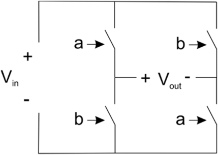

The half H bridge, shown in Fig. 8.23, is often used in power and drive circuits. As the name implies, it provides two switches that allow one connection to be switched between terminals with opposite polarities. In a motor application, an LC tank is typically added in series to the bottom loop to create oscillations when the motor is not connected to the high power supply voltage.

An H bridge IC combines the H bridge function with driver circuits that can provide the large currents required for inductive loads. The L298 [56] provides two H bridges. It operates at a supply voltage of up to 46 V and can supply DC output current up to 4 A. Its control inputs have a very high VIL = 1.5 V, the maximum voltage that is considered a valid logic 0; this high voltage provides good noise immunity. The DRV8844 provides four half H bridges which can be configured in various combinations of half and full H bridges.
We will start with a brushed motor speed controller. As shown in Fig. 8.24, a brushed DC motor uses a commutator to chop the DC supply. Brushes connect the electromagnets to the commutator to supply alternating polarities. The switching state of the electromagnets is timed to attract to and repel from the poles of the permanent magnets to spin the shaft.

The motor speed controller application consists of three tasks: a control law task, a command input task, and a motor command output task.
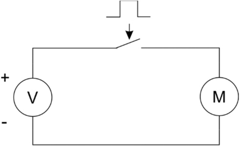
The simplest motor speed controller, shown in Fig. 8.25, operates open loop—it drives the motor based on a speed command without checking the actual speed of the motor. In this case, the control law maps a command speed to a PWM level. The control law can take one of several forms. The simplest open-loop control law is a linear function that maps the command speed to a PWM duty cycle value. However, the motor may not operate entirely linearly. We can create an open-loop control law to adjust for motor nonlinearities using either a functional description or table lookup.
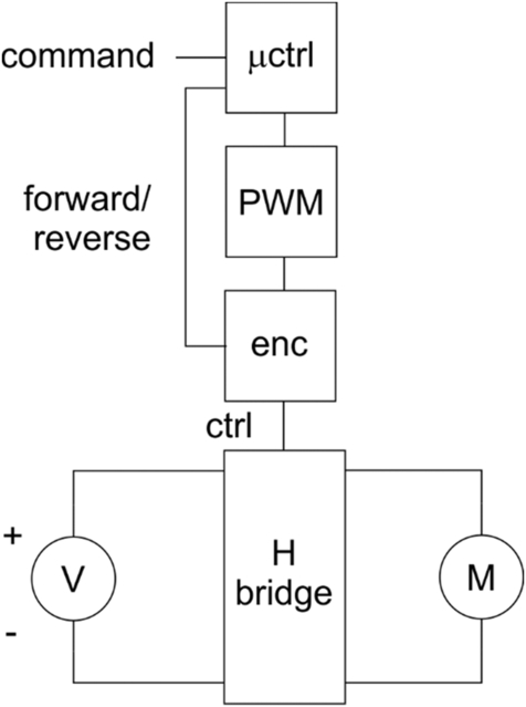
The motor M is connected to its power supply VM through an H bridge. We use the two control inputs a, b of the H bridge to both control the polarity of the motor voltage and to modulate its pulse width. If a = b = 0, the motor will be disconnected from its power supply. We can use an encoder to turn the PWM duty cycle waveform into the H bridge control signals; a separate input determines whether the motor runs in forward or reverse.
If we allow the motor to operate in either direction, we need to be careful when we switch rotational directions. Commanding the H bridge to immediately from forward to reverse configuration can cause excessive transients that can damage components. We can design the logic of the H bridge encoder to provide a disconnected mode. We can then design the control law with short-term memory to insert a dead zone in between changes in direction.
The sample rate for the microcontroller should be fast relative to the top rotational speed of the motor.
Fig. 8.26 shows the block diagram for a closed-loop brushed motor speed controller. We use the microcontroller to execute the control law. It reads the shaft encoder at sense to monitor the speed of the motor.

A typical software/hardware partition for the motor controller computes the control law in software, performs the PWM function primarily in hardware, and counts shaft rotation events in hardware.
We can sense the speed of the motor using the shaft encoder of Section 3.11. The number of divisions on the encoder disk determines the precision with which we can measure the shaft RPM.
We need to choose two parameters for the pulse-width modulation operation: the PWM period and the PWM duty cycle resolution. The period should be small relative to the time constant of the motor, which is determined by the motor's inductance and internal resistance. These parameters are not always provided on motor data sheets but they can be measured. The PWM period is typically short enough to allow several PWM periods in one revolution of the motor at its maximum speed.
The rate of shaft encoder pulses varies with the motor speed. Using a hardware counter to count the shaft pulses in an interval eliminates the interrupt handler overhead that would be required for each encoder pulse.
The control law sample rate should be high enough to provide proper tracking of the commanded speed. The sample rate in turn determines the required execution period Tlaw for the control law task. If we use an interrupt service routine to execute the control law, we can find the total task execution time as the combination of the interrupt response time and the control law function execution time:
The total CPU utilization is then

The numerical precision required for the control law function depends in part on the range of motor speeds at which the control system must operate. For a speed range [Rmin, Rmax], the dynamic range of the values must be at least ⌈ log2(Rmax − Rmin)⌉. We must also take into account the controller gains, which increase the dynamic range to ⌈ log2Kpid(Rmax − Rmin)⌉ where Kpid is the maximum of the three controller gains. Our control law does not include any division which helps to limit the required dynamic range. Many small microcontrollers support hardware floating-point operations. If the microcontroller does not support floating-point arithmetic, we can carefully design the code and the controller parameters to use entirely integer arithmetic. Multiplying and dividing by powers of two allows us to use bit-level operations as substitutes, although at the cost of reduced accuracy of the control law, since the parameters must be rounded to powers of two.
Brushless DC motors were made possible by high-speed power electronics. As shown in Fig. 8.27, a brushless motor does not have a mechanical commutator—it uses a controller to directly energize the coils of the motor [10]. The fixed magnets are on the motor shaft; the electromagnets push and pull relative to those magnets to spin the motor shaft. The figure shows a three-phase motor with two phases per coil. The three ABC leads allow each pair of coils to be separately energized. The controller must precisely time the coil energization. Directly controlling the coils allows the controller to more precisely control the position and speed of the shaft.

As with brushed motors, we use pulse-width modulation to regulate the motor speed. Whenever the PWM duty interval is active, we must provide the energizing signals to the coils at the appropriate times. Each phase of the commutation period TC is used in both push and pull mode by applying positive and negative voltages.
Fig. 8.28 shows the timing of the drive signals for the brushless motor phases. The motor coils are configured as a Y circuit with a common connection. The connections for the three phases are labeled A, B, C. The positive energizing voltages are labeled H and the negative energizing voltages as L. Each phase also has an undriven dead time interval, shown in the figure as Z regions. Fig. 8.29 illustrates the operation of the motor at three times shown in the timing diagram. Switching the coils between high side and low side in the proper order provides a rotating magnetic field that pulls the rotor's permanent magnet around the motor.


As with the brushed DC motor, the pulse-width modulator signal is used as input to the decoder that controls the H bridge. But in this case, the code used to control the H bridge configuration is determined by the shaft position sensor. While we could use a shaft encoder, the motor itself provides sensing opportunities. In a sensor-controlled brushless motor, a set of Hall effect sensors are used to determine when the electromagnets pass known points. In a sensorless brushless motor, the back EMF produced by the motor can be used to determine its position. In this case, the back EMF is sensed as a voltage on an undriven terminal of the motor using an analog-digital converter. We can compare the back EMF to a reference voltage to generate a zero-crossing event.
Brushless motor controllers must run at much higher rates than are required for brushed motor controllers—the motor must be actively controlled within fractions of a revolution. The commutation scheme of Fig. 8.28 changes configurations every 60 degrees, requiring a task period of 6 × rev/s.
Two tasks can be used to operate the motor. One task performs commutations that change which coils are energized. This task is controlled by a timer whose timeout interval is based on an estimate of the motor speed. Another task monitors zero crossings of the back EMF and performs control law calculations to update the commutation time. Zero crossings are handled as events. If the motor is spinning at the commanded speed, the zero crossing should occur at the middle of the commutation period. If the zero crossing occurs early, for example, the motor is running too slow and the commutation period needs to be shortened. A separate startup control algorithm is usually required to get the motor up to speed.
The rate at which the commutation and zero crossing tasks execute depends on motor speed. We can find the worst-case CPU utilization based on the minimum commutation period, which for a 60 degrees control scheme is equal to Tmin = 6/revmax . Given a commutation execution time tc and zero crossing execution time tz, the worst-case CPU utilization is

A wide range of microcontrollers have been designed with brushless motor control in mind. The Microchip Technology PIC16F [37] includes an analog-digital converter, analog comparator, voltage reference, and multiple timers; it performs integer arithmetic. The TI TMS320F28004x microcontroller [71] uses a 32-bit CPU with floating-point arithmetic, a separate control law accelerator with floating-point arithmetic, three analog/digital converters, seven windowed comparators, and 16 extended PWM units.
Further Reading
Nisagara and Torres [44] and Brown [10, 11] discuss brushless DC motor control.
Questions
- Q8.1 What must be added to the jack detector circuit of Section 5.14 to create a complete interface?
- Q8.2 What must be added to the electret microphone amplifier circuit of Section 4.11 to create a complete interface?
- Q8.3 We need to build an 8-tap digital filter with 16-bit data values to run at a rate of 40 kHz. Is an 8-bit, 32 MHz microcontroller with 256 bits of RAM likely to be able to implement the filter in software? Explain.
- Q8.4 Which is likely to be a cheaper way to implement a two-pole low-pass filter: analog or digital programmable logic? Explain.