
Appendix
Applications to Optoelectronics Materials
Hideo Aida Namiki Precision Jewel Co., Ltd, NJC Institute of Technology, Adachi, Tokyo, Japan, Kyushu University, Fukuoka, Japan
Various applications of recent information technology are supported by sophisticated device technology. With ongoing changes to technology, functional materials, including semiconductors, are needed to develop high-performance, intricate device technology, and the physical properties of the substrate material are becoming more important for maintaining technical advantages. In this chapter, the importance of sapphire, GaN, and diamond, which have recently gained attention as single-crystal materials for next-generation optoelectronics devices, is explained, and the processing of each material by chemical mechanical processing (CMP) is introduced.
A.1 Importance and expectation of next-generation optoelectronics materials
Human beings have a long history of processing close-at-hand materials and creating tools for daily tasks. For example, stone accessories and knives were created in the Stone Age, and subsequent advances in technology have seen commonly utilized materials change from stone to ceramics and glass, with a simultaneous change in processing technologies; lens processing in the Middle Ages is one such example. Materials such as ceramics and glass have a proven degree of durability and water resistance and have been used for routine daily applications for a long time. This familiarity has prompted the ongoing development of reinforced ceramics and crystal materials for applications in which strength, stability, workability, and transparency are required or become required for a society at a given time. The relatively recent development of semiconductors, which ushered in the current information-technology generation, also demanded a range of functional requirements such as optimal electrical conduction properties, insulating properties, electric-field characteristics, and transparent conductive properties in addition to strong abrasion and corrosion resistance to fabricated devices. At present, to realize next-generation compound semiconductor devices capable of operating under even more severe environments, materials with a higher heat conductivity, heat resistance, and chemical stability are required.
Against this background, sapphire, GaN, and diamond are promising single-crystal materials for next-generation optoelectronics devices. Sapphire is commonly used as a substrate for growing group-III nitride semiconductor device films, but it is becoming an essential substrate for the growth of devices such as white light-emitting diodes (LEDs). GaN substrates are expected to make next-generation environmentally resistant high-speed and high-voltage devices possible, and it is attracting attention as a substrate for power electronics. The use of diamond as a substrate is expected to realize further technical advantages in semiconductor devices because it is the ultimate semiconductor substrate. Diamond substrates are still under development, with a range of issues in regard to its practical use as a large-area substrate, but active studies of its practical use are likely in the near future. A comparison of the device performance obtained for devices grown on GaN, diamond, and existing semiconductor materials such as Si, GaAs, and InP is shown in Figure A.1. These new materials (GaN and diamond) are expected to result in improved device performances.
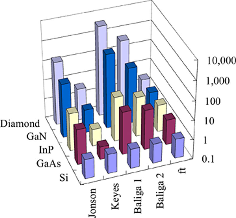
Figure A.1 Device performance expected with next-generation optoelectronics materials
A.2 Difficulties in CMP of next-generation optoelectronics materials
Characteristics of the chemical mechanical polishing (CMP) processing for the next-generation single-crystal optoelectronics materials of sapphire, GaN, and diamond in terms of the hardness of each material and its chemical stability are presented here. CMP involves removing material from a surface through mechanical and chemical action without introducing processing strain into the material. The mechanical action between the abrasive and the workpiece is related to the type of material, hardness, quality, shape, and diameter of abrasives and the concentration of such abrasives in a slurry; whereas the chemical action relates to the pH of the chemical solvent and the etching performance for the workpiece and so on. Because the CMP processing characteristics are the result of a complex interplay of various factors, a wide range of choices is available for the abrasive compound used in CMP.
The most versatile abrasive compound is a colloidal silica slurry. It is possible to obtain a surface free from processing-induced strain by using a colloidal silica slurry even if the material is a chemically stable crystal [1]. Colloidal silica is generally used for the CMP of sapphire substrates [1,2], and its effectiveness for the CMP of GaN has recently been reported [3].
Doy [1] derived the following relationship between the processing rate MRR, hardness H of the workpiece, and processing pressure p:
 (A.1)
(A.1)from which it can be seen that a higher processing pressure is required for a harder workpiece. As shown in Table A.1, sapphire is harder than Si, but we see that the values for GaN are not as accurate as the others because crystal growth is still under development. The data in the literature for the hardness for GaN, for example, suggest that it is somewhere close to or twice that of silicon. Improvements in the growth techniques of bulk crystals are likely to lead toward the true value of the hardness. The most recent study [5] gives the GaN hardness as twice that of silicon; the general consensus is that GaN is slightly softer than sapphire. Based on equation (A.1), the processing pressure will be an important determining parameter in CMP, especially for the hard materials.
Table A.1
Vickers Hardness of Si, Sapphire, and GaN (GPa)
| Sapphire | 28 [4], 22.5 |
| GaN | 20–21.2 [5], 21 [6], 18–20 [7], 18 ± 1 [8], 12 ± 2 [9], 12.3 [10], 11 [11–13] |
| Si | 12 [11–13], 9 [7] |
The CMP processing rate can also be represented the formula proposed by Preston [14]:
where k is a constant that depends on the conditions of the abrasive environment (i.e., Preston’s constant), and v is the relative speed between the workpiece and the lap. The processing efficiency is thus determined by the interplay between k, v, and p. Note that k is mainly determined by the action between the workpiece and the abrasive compound, while p and v are factors determined by the removal conditions dictated by the machine parameters. Therefore, the design of the abrasive machine is important, but the processing equipment offer little flexibility when a material to which a high pressure has to be apply is used because of the high hardness mentioned earlier. For this reason, careful attention must be paid to the chemical action, but for materials such as sapphire, GaN, and diamond, which have a high thermal/chemical stability, the improvement in the removal rate by chemical action is limited.
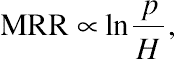
The processing rates for Si, sapphire, and GaN are compared in Figure A.2. The removal rate of sapphire is 1/10 of that of silicon, and sapphire is widely regarded as a hard-to-work substrate. In the case of GaN, however, the best obtainable processing rate is only 1/100 of that of sapphire. Thus, if sapphire is a hard-to-process material, then GaN could well be said to be a super-hard-to-process material. For diamond, a CMP removal rate has yet to be established, but preliminary experimental data estimate the removal rate to be 1/1,000 to 1/10,000 of that of silicon.
As noted, sapphire, GaN, and diamond are materials with an extremely high hardness and high thermal/chemical stability in comparison to existing and past substrate materials, and it is fair to say that substrate processing techniques for these materials will also be extremely difficult.
A.3 Case study I: CMP of sapphire
Sapphire substrates are presently in great demand because they are the main substrate for the fabrication of GaN-based optoelectronics devices [15-18]. In most cases, c-plane (0001) sapphire substrates are used for nitride epitaxy, and it is essential to prepare atomically well-controlled, damage-free surfaces to obtain high-performance epitaxial nitride films for devices such as light-emitting diodes (LEDs) and laser diodes (LDs).
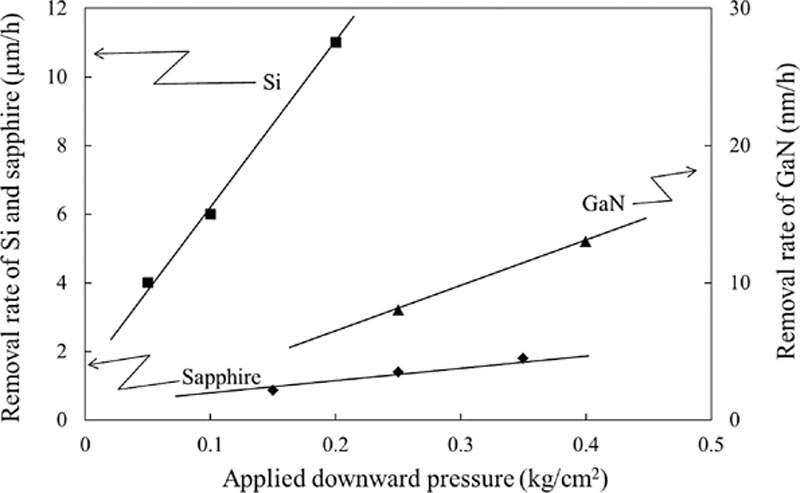
Figure A.3 shows three- and two-dimensional views of the unit cell of sapphire crystals, and the basic physical properties of sapphire are listed in Table A.2. Sapphire crystals belong to the trigonal system and have an axis of mirror rotation system of the sixth order  , three axes of
  . The sapphire crystal lattice consists of bivalent oxygen ions and trivalent aluminum ions [19].
Table A.2
Physical Properties of Sapphire
| Density (×103 kg/m3) | 3.98 |
| Crystallization system | hexagonal |
| Compressive strength (GPa) | 3.05–3.41 |
| Hardness | C⊥HK: 1525–1660 C// HK: 1670–2000 |
| Young’s modulus (GPa) | 363 |
| Tensile strength (GPa) | 0.49 |
| Coefficient of thermal expansion (×10−6 K−1) | C⊥: 5.0 C//: 6.7 |
| Resistivity (Ω m) | 1013 |
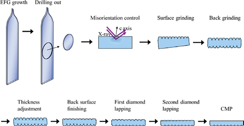
The typical wafering process, which starts from a ribbon-shaped sapphire crystal grown by the edge-defined, film-fed growth method, is shown in Figure A.4. A circular-shaped crystal almost 2 inches in size is drilled out from the ribbon, and the misorientation angle of the sapphire crystal is controlled using XRD. Because the misorientation angle strongly affects the growth mechanism of metal organic chemical vapor phase deposition (MOCVD)-grown GaN thin films, it is essential that it is corrected. (The effect of the misorientation angle on nitride epitaxy and LED performance has been described in detail elsewhere [22-27]). A two-step lapping process is then applied to the crystal using, for example, 2- and 0.5-μm diamond abrasives, which is followed by CMP with colloidal silica in an alkaline solution to obtain a surface free of scratches and damage.
The typical surface conditions after CMP under the typical polishing conditions given in Table A.3 are shown in Figure A.5. Over the 5 × 5 μm2 area of the substrate in the AFM image in Figure A.5, the surface roughness Ra is 0.08 nm; markedly smooth surfaces have been demonstrated by using CMP with a colloidal silica slurry [21]. It might be surprising that softer SiO2 particles are able to remove the harder sapphire material, but the polishing of sapphire proceeds through an intermediate product, aluminum silicate dehydrate, as shown by the following chemical reaction [2]:
Table A.3
Polishing Conditions for Sapphire
| Platen rotation speed | (rpm) | 50 |
| Carrier rotation speed | (rpm) | 40 |
| Applied pressure | (kg/cm2) | 0.3 |
| Diameter of platen | (mm) | 380 |
| Polishing pad type | Suede type | |
| Slurry type | Colloidal silica | |
| Slurry pH | 10.5 | |
| Abrasive particle size | (nm) | 40 |
| Abrasive concentration | (%) | 20 |

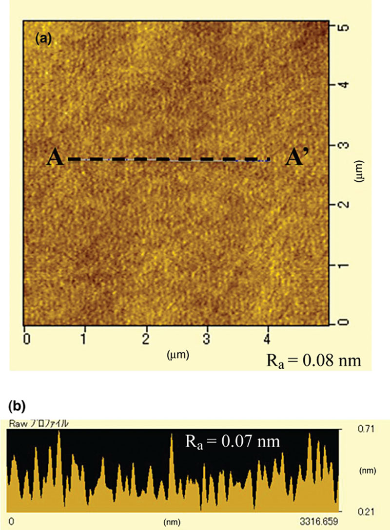
Figure A.5 Atomically flat sapphire substrate finished by CMP process: (a) AFM image of 5 × 5 μm2 area and (b) cross-sectional image of A–A’ line [22]
We previously presented theoretical calculations of the surface conditions after CMP [21,28]. Figure A.6a illustrates the theoretical consideration of an ideal atomic structure of a sapphire crystals with a single bilayer step. The simplified model of a miscut sapphire surface is shown as a sphere with a radius equal to 1/6 of the c-axis of sapphire [20,29]. Figure A.6b and c show the cross-section of the modeled misoriented sapphire crystals in detail. When the surface consisting of a single bilayer structure corresponding to the periodical step-and-terrace structure is modeled as shown in Figure A.6b, the relationship between the misorientation angle θ, terrace width w, and step height h is given by
 (A.3)
(A.3)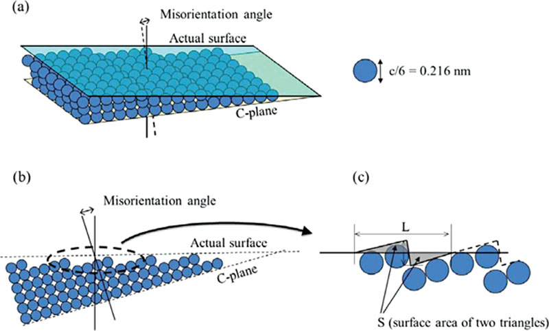
Figure A.6 Ideal surface model of atomic step-and-terrace structure due to misorientation: (a) three-dimensional image, (b) cross-sectional image of atomic steps, and (c) enlarged image of cross-section for the calculation of theoretical surface roughness [22]
where h corresponds to the height of one bilayer, which is 0.216 nm for sapphire. Therefore, the substrate Ra for sapphire is calculated theoretically as a function of the misorientation angle and single bilayer height as
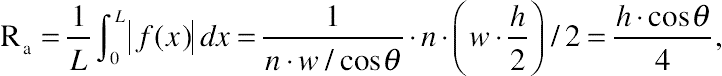 (A.4)
(A.4)where n is the number of step-and-terrace structures within the measured surface length L. The theoretical Ra for the ideal single bilayer step-and-terrace structure is calculated as 0.054 nm for sapphire when the misorientation angle is negligibly small. The smooth sapphire substrate finished by CMP in Figure A.5 had an Ra of 0.08 nm, meaning that an almost ideal level of atomic surface roughness can be obtained by CMP with colloidal silica.
A.4 Case study II: CMP of GaN
Gallium nitride (GaN)-based semiconductors are promising materials for blue LDs, LEDs, and high-power, high-frequency field-effect transistors (FETs) [15,16]. Epitaxial layers of III-nitrides, such as GaN, are also commonly grown on sapphire substrates [17,18]. However, the large lattice mismatch and difference in the thermal expansion between the sapphire substrate and III-nitride films often leads to a poor epitaxial film quality that severely limits the performance of various devices. In this regard, single-crystal bulk GaN substrates are a promising candidate for replacing sapphire substrates and improving the III-nitride device performance drastically by enabling homoepitaxial growth of III-nitride device films. The basic physical properties of GaN are given in Table A.4. Single crystals of bulk GaN can be grown by high-pressure solution growth (HPGS) [30], hydride vapor phase epitaxy (HVPE) [31,32], ammonothermal growth [33], and liquid phase epitaxy (LPE) [34].
Table A.4
Physical Properties of GaN
| Band gap (eV) | 3.4 |
| Breakdown electric field (MV/cm) | 2.5 |
| Carrier saturation velocity (×107 cm/s) | 2.0 |
| Electron mobility (cm2·V−1·s−1) | ∼2000 |
| Relative permittivity | 8.9 |
| Thermal conductivity (W·cm−1·K−1) | 1.5 |
After the growth of a bulk crystal, the crystal will need to undergo a wafering process that includes cutting, grinding, polishing, and chemical etching. To obtain high-performance thin-film devices on GaN substrates using homoepitaxy, it is essential to achieve a substrate surface free of scratches and damage. Therefore, the final step of the wafering process plays an extremely important role in determining the quality of the subsequent homoepitaxial GaN films and related devices.
The first study of the CMP processing of GaN with colloidal silica was reported by Tavernier and colleagues [35]. Although the colloidal-silica-based slurry was able to polish the nitrogen face of GaN, the gallium face had an extremely low polishing rate due to chemical inertness. However, this finding did provide important evidence that softer silica particles can remove the harder GaN without inducing subsurface damage. After Tavernier report [35], we paid careful attention to the small changes in the density of the surface scratches and found that the gallium face of GaN could be polished with a colloidal silica slurry. The removal rate we obtained was relatively low, 17 nm/h [3], because the Ga-face of GaN is inert to almost all chemical solutions [36].
Here, we introduce our recent research on CMP of GaN substrates [3]. The experiment was conducted as follows. A GaN crystal was fixed onto a ceramic wafer carrier with the gallium face up. Prior to CMP, grinding was performed to remove the as-grown surface roughness and to make the substrate flat. Grinding was followed by two steps of mechanical lapping processes conducted using progressively smaller-sized diamond abrasives: a 2-μm diamond particle abrasive for the first step, and a 0.5-μm abrasive for the second step. After the diamond lapping, CMP with a colloidal-silica-based slurry was performed using a table-type polishing machine. The detailed conditions of the CMP process, which used a commercially available colloidal silica slurry, are summarized in Table A.5.
Table A.5
Polishing Conditions for GaN
| Platen rotation speed | rpm | 50 |
| Carrier rotation speed | rpm | 40 |
| Applied pressure | kg/cm2 | 0.4 |
| Diameter of platen | mm | 300 |
| Polishing pad type | Suede type | |
| Slurry type | Colloidal silica | |
| Slurry pH | 10.5 | |
| Abrasive particle size | nm | 40 |
| Abrasive concentration | % | 40 |
Figure A.7 shows an AFM image of the GaN surface after CMP, which achieved an atomically flat surface with a surface roughness of 0.1 nm. Carefully checked the changes in the surface during the CMP, as shown in Figure A.8, by observing the GaN surface every 2 h. Of the three steps in the scratch removal process, surface scratches are removed in the first step, and a surface with fewer scratches appears; in the second step, fine scratches on the surface can be seen in a microscope observation; and in the third step, which begins after 24 h, the density of the scratches starts to decrease.
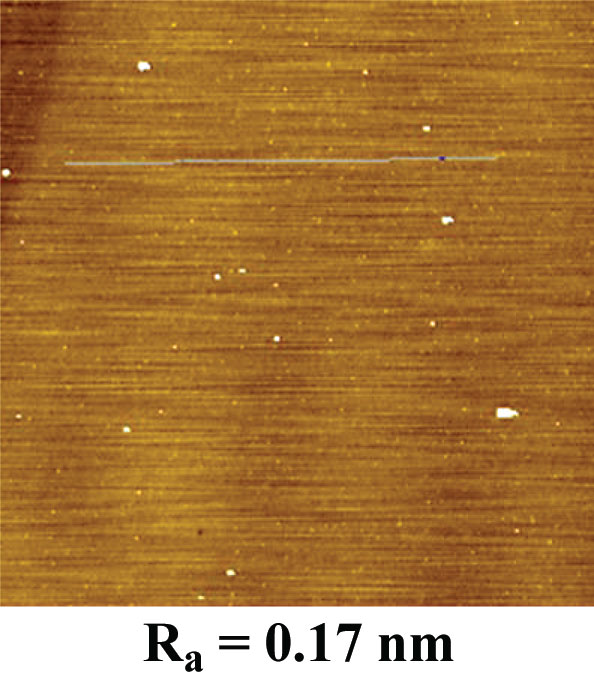
Figure A.7 AFM images of GaN substrate surface after 150 h of CMP processing (image size = 5 × 5 μm2) [3]

Figure A.8 Surface morphologies of GaN substrate during the CMP process (image size = 60 × 60 μm2) [3]
The change in the surface roughness is shown as a function of the CMP process time in Figure A.9. A nominal decrease in the surface roughness to 0.6 nm from an initial roughness of 0.7 happens during the first step of CMP, and then the Ra suddenly increases to 1.7 nm in the second step of CMP. After this, it decreases to 0.17 nm with increasing CMP time. The behavior of the Ra during the CMP seems to provide strong support of etching the subsurface damage layers and their removal.
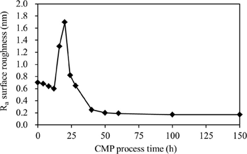
Figure A.9 Ra surface roughness measured in a 5 × 5 μm2 area plotted as a function of CMP process time [3]
It is important to verify the complete absence of subsurface damage. However, microscope and AFM observations of the subsurface cannot directly detect the subsurface damage, and so the development of a specialized observation method is important. In the case of GaN, cathode luminescence (CL) imaging is effective for visualizing subsurface damage because in a CL image, dislocations appear as dark areas and act as nonradiative recombination sites, which results in a decrease in the luminescence intensity, thus allowing subsurface damage induced by the polishing process to be imaged using CL [37]. The actual observation results are shown in Figure A.10. The subsurface damage can be seen clearly as dark lines in the CL images, although the dislocations in the GaN crystal itself are dark spots. These images provide strong verification that damage can be removed by using the colloidal silica slurry. Interestingly, although almost all the surface scratches were removed after 40 h of CMP, some subsurface damage remained even after 90 h of CMP. In all, it took 150 h to remove all the subsurface damage of the GaN substrate. On the basis of this study, we proposed a schematic model of the removal of scratches and damaged layers over 150 h of CMP of Ga-faced GaN substrates. Further information on the CMP of GaN is provided elsewhere [3,28,38].

A.5 Case study III: CMP of diamond
Diamond is the ultimate semiconductor material owing to characteristics that make it indispensable for improving semiconductor performance. The basic physical properties of diamond are given in Table A.6. The synthesis of large-area diamond substrates is currently under development, so it will be some time until diamond devices are realized in industry. However, to prepare for a future in which industrial-scale diamond substrates are available, it is worth developing a surface treatment process for diamond to create epitaxy-ready surfaces. Little research on the CMP of diamond has been conducted, but we discuss here its possibilities.
Table A.6
Physical Properties of Diamond
| Density (×103 kg/m3) | 3.52 |
| Crystallization system | Diamond |
| Compressive strength (GPa) | 6–11 |
| Hardness | HK: 6,000–11,000 |
| Young’s modulus (GPa) | 1,000–1,100 |
| Tensile strength (GPa) | 1–4 |
| Coefficient of thermal expansion (×10−6 K−1) | 1 |
| Resistivity (Ω m) | 102–1018 |
We applied the conventional CMP conditions with a commercially available colloidal silica slurry to a diamond substrate that was 4 × 4 mm2 in size. Figure A.11 shows the surface of the diamond substrate before and after CMP. Before CMP, the surface exhibits some straight scratches that are related to the thermomechanical preprocessing procedure, but these scratches are removed by the CMP. However, numerous pits are created on the surface, which indicates that a chemical reaction between the colloidal silica slurry and diamond surface. Thus, the conventional colloidal silica slurry may not be suitable for the CMP of diamond.
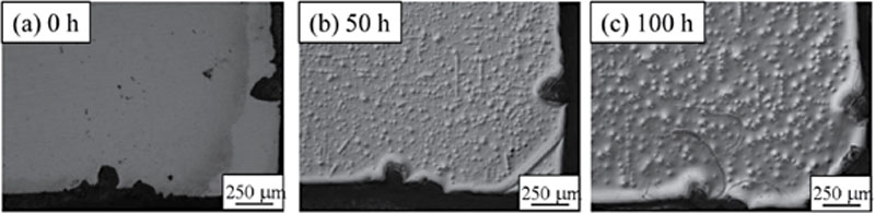
Figure A.11 Surface of diamond (a) before, (b) during, and (c) after CMP with colloidal silica slurry
Figure A.12 shows the diamond surface before and after CMP with a slurry optimized for diamond. In this case, mechanically induced scratches were removed without generating pits; however, it took more than 100 h to obtain the final surface for the relatively small substrate (4 × 4 mm2). A simple estimation considering the surface area effect gives the process time of a 2-inch diamond substrate as 12,200 h (owing to the surface area increasing by a factor of 122). While the result in Figure A.12 indicates that it is possible to apply CMP to a diamond surface, further advanced processing techniques will need to be developed.
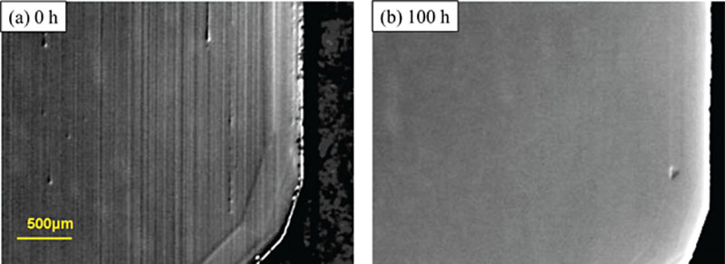
Figure A.12 Surface of diamond (a) before and (b) after CMP with a slurry optimized for diamond CMP
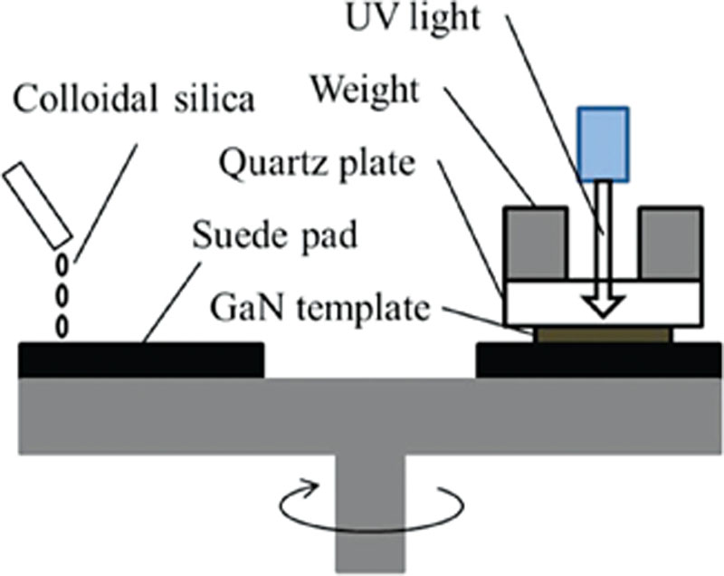
Figure A.13 Schematic diagram of the experimental setup for UV-assisted CMP
A.6 Case study IV: advanced CMP for GaN
In many cases, surface oxidation is a key to improving the CMP performance, which has been confirmed for CMP of GaN substrates in our recent research [28,39]. The biggest issue, however, is how to promote surface oxidation during CMP. To exploit this mechanism, it is essential to develop a new CMP method or machine to achieve accelerated in situ oxidation of the GaN surface. In this section, we propose two approaches: ultraviolet (UV)-assisted CMP and atmosphere-controlled CMP with a closed bell-jar CMP machine. The former approach is expected to increase the density of hydroxyl radicals (OH*) in the reaction system, while the latter is expected to increase the amount of dissolved oxygen in the CMP slurry. Both will contribute to rapid surface oxidation, resulting in an improved GaN removal rate.
UV-Assisted CMP
Figure A.13 shows the experimental setup for UV-assisted CMP. The interface between GaN thin films of a few micrometers in thickness grown on double-side polished 2-inch sapphire substrates and the polishing pad were irradiated by UV light through the backside of the sapphire substrate. A markedly higher GaN removal rate (around five times) was observed with UV-assisted CMP as shown in Figure A.14. The hydroxyl radicals (OH*) generated during the UV-assisted CMP process, act as an oxidizing agent to enhance surface oxidation reactions, resulting in a higher removal rate of the Ga-faced GaN.
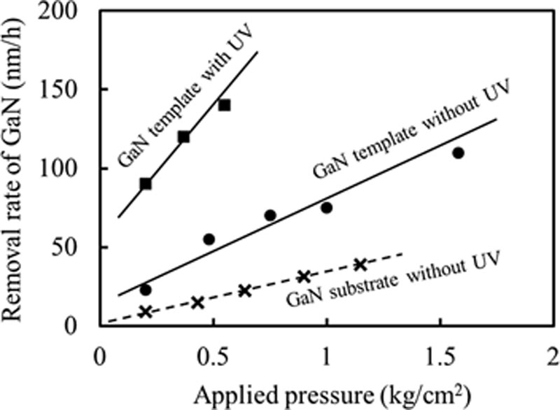
Figure A.14 GaN removal rate as a function of the applied pressure with and without UV assist
Atmosphere-Controlled CMP
The polishing efficiency of GaN can also be improved by controlling the environmental conditions, using a “bell-jar” to create a sealed environment [40–43]. A cross-section of the bell-jar CMP system is shown in Figure A.15, in which the atmospheric pressure is easily controlled by the gas cylinder pressure. Figure A.16 shows the polishing characteristics of a GaN substrate using this system. Polishing under high-pressure oxygen and high-pressure air atmospheres increases the polishing rate in comparison to that of typical CMP under atmospheric pressure. These experimental results are significant for demonstrating that the presence of oxygen is advantageous for polishing, although further research is required to obtain more details about the mechanism. The first interesting phenomena concerning the GaN removal rate improvement with a bell-jar CMP system have been obtained.
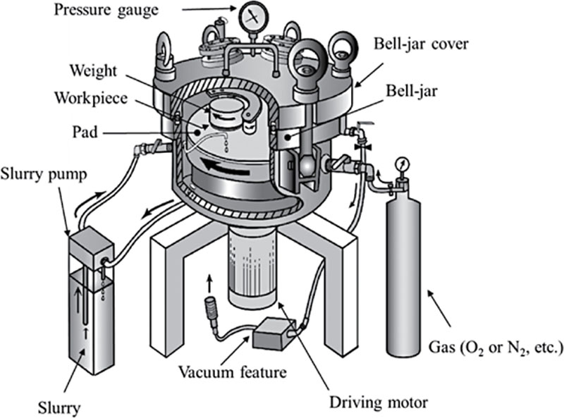
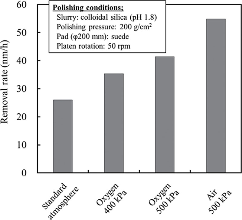
Figure A.16 Polishing characteristics of the GaN substrate with the bell-jar CMP system
..................Content has been hidden....................
You can't read the all page of ebook, please click here login for view all page.