6
Noise in Networks and Systems
Many electrical circuits generate some kind of noise internally. The most well-known kind of noise is thermal noise produced by resistors. Besides this, several other kinds of noise sources can be identified, such as shot noise and partition noise in semiconductors. In this chapter we will describe the thermal noise generated by resistors, while shot noise is dealt with in Chapter 8. We shall show how internal noise sources can be transferred to the output terminals of a network, where the noise becomes observable to the outside world. For that purpose we shall consider the cascading of noisy circuits as well. In many practical situations, which we refer to in this chapter, a noise source can adequately be described on the basis of its power spectral density; this spectrum can be the result of a calculation or the result of a measurement as described in Section 5.4.
6.1 WHITE AND COLOURED NOISE
Realization of a wide-sense stationary noise process N(t) is called white noise when the power spectral density of N(t) has a constant value for all frequencies. Thus, it is a process for which
![]()
holds, with N0 a real positive constant. By applying the inverse Fourier transform to this spectrum, the autocorrelation function of such a process is found to be
![]()
The name white noise was taken from optics, where white light comprises all frequencies (or equivalently all wavelengths) in the visible region.
It is obvious that white noise cannot be a meaningful model for a noise source from a physical point of view. Looking at Equation (3.8) reveals that such a process would comprise an infinitely large amount of power, which is physically impossible. Despite the shortcomings of this model it is nevertheless often used in practice. The reason is that a number of important noise sources (see, for example, Section 6.2) have a flat spectrum over a very broad frequency range. Deviation from the white noise model is only observed at very high frequencies, which are of no practical importance.
The name coloured noise is used in situations where the power spectrum is not white. Examples of coloured noise spectra are lowpass, highpass and bandpass processes.
6.2 THERMAL NOISE IN RESISTORS
An important example of white noise is thermal noise. This noise is caused by thermal movement (or Brownian motion) of the free electrons in each electrical conductor. A resistor with resistance R at an absolute temperature of T has at its open terminals a noise voltage with a Gaussian probability density function with a mean value of zero and of which the power spectral density is

where
![]()
is the Boltzmann constant and
![]()
is the Planck constant. Up until frequencies of 1012 Hz the expression (6.3) has an almost constant value, which gradually decreases to zero beyond that frequency. For useful frequencies in the radio, microwave and millimetre wavelength ranges, the power spectrum is white, i.e. flat. Using the well-known series expansion of the exponential in Equation (6.3), a very simple approximation of the thermal noise in a resistor is found.
Theorem 9
The spectrum of the thermal noise voltage across the open terminals of resistance R which is at the absolute temperature T is
![]()
This expression is much simpler than Equation (6.3) and can also be derived from physical considerations, which is beyond the scope of this text.
6.3 THERMAL NOISE IN PASSIVE NETWORKS
In Chapter 4 the response of a linear system to a stochastic process has been analysed. There it was assumed that the system itself was noise free, i.e. it does not produce noise itself. In the preceding section, however, we indicated that resistors produce noise; the same holds for semiconductor components such as transistors. Thus, if these components form part of a system, they will contribute to the noise at the output terminals. In this section we will analyse this problem. In doing so we will confine ourselves to the influence of thermal noise in passive networks. In a later section active circuits will be introduced.
As a model for a noisy resistor we introduce the equivalent circuit model represented in Figure 6.1. This model shows a noise-free resistance R in series with a noise process V(t), for which Equation (6.6) describes the power spectral density. This scheme is called Thévenin's equivalent voltage model. From network theory we know that a resistor in series with a voltage source can also be represented as a resistance R in parallel with a current source. The magnitude of this current source is
![]()
In this way we arrive at the scheme given in Figure 6.2. This model is called Norton's equivalent current model. Using Equations (4.27) and (6.7) the spectrum of the current source is obtained.
Theorem 10
The spectrum of the thermal noise current when short-circuiting a resistance R that is at the absolute temperature T is
![]()
In both schemes of Figures 6.2 and 6.1, the resistors are assumed to be noise free.
When calculating the noise power spectral density at the output terminals of a network, the following method is used. Replace all noisy resistors by noise-free resistors in series with a voltage source (according to Figure 6.1) or parallel with a current source (according to Figure 6.2). The schemes are equivalent, so it is possible to select the more convenient of the two schemes. Next, the transfer function from the voltage source or current source to the output terminals is calculated using network analysis methods. Invoking Equation (4.27), the noise power spectral density at the output terminals is found.
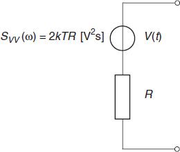
Figure 6.1 Thévenin equivalent voltage circuit model of a noisy resistor

Figure 6.2 Norton equivalent current circuit model of a noisy resistor
Example 6.1:
Consider the circuit presented in Figure 6.3. We wish to calculate the mean squared value of the voltage across the capacitor.
Express Vc(ω) in terms of V using the relationship
![]()
and


Figure 6.3 (a) Circuit to be analysed; (b) Thévenin equivalent model of the circuit
Invoking Equation (4.27), the power spectral density of Vc(ω) reads
![]()
and using Equation (4.28)
![]()
![]()
When the network comprises several resistors, then these resistors will produce their noise independently from each other; namely the thermal noise is a consequence of the Brownian motion of the free electrons in the resistor material. As a rule the Brownian motion of electrons in one of the resistors will not be influenced by the Brownian motion of the electrons in different resistors. Therefore, at the output terminals the different spectra resulting from the several resistors in the circuit may be added.
Let us now consider the situation where a resistor is loaded by a second resistor (see Figure 6.4). If the loading resistance is called RL, then similar to the method presented in Example 6.1, the power spectral density of the voltage V across RL due to the thermal noise produced by R can be calculated. This spectral density is found by applying Equation (4.27) to the circuit of Figure 6.4, i.e. inserting the transfer function from the noise source to the load resistance

Note the confusion that may arise here. When talking about the power of a stochastic process in terms of stochastic process theory, the expectation of the quadratic of the stochastic process is implied. This nomenclature is in accordance with Equation (6.13). However, when speaking about the physical concept of power, then conversion from the stochastic theoretical concept of power is required; this conversion will in general be simply multiplication by a constant factor. As for electrical power dissipated in a resistance RL, we

Figure 6.4 A resistance R producing thermal noise and loaded by a resistance RL
have the formulas ![]() , and the conversion reads as
, and the conversion reads as
![]()
For the spectral density of the electrical power that is dissipated in the resistor RL we have
![]()
It is easily verified that the spectral density given by Equation (6.15) achieves its maximum when R = RL and the density is
![]()
Therefore, the maximum power spectral density from a noisy resistor transferred to an external load amounts to kT/2, and this value is called the available spectral density. It can be seen that this spectral density is independent of the resistance value and only depends on temperature.
Analogously to Equation (6.6), white noise sources are in general characterized as
![]()
In this representation the noise spectral density may have a larger value than the one given by Equation (6.6), due to the presence of still other noise sources than those caused by that particular resistor. We consider two different descriptions:
- The spectral density is related to the value of the physical resistance R and we define Re = R. In this case Te is called the equivalent noise temperature; the equivalent noise temperature may differ from the physical temperature T.
- The spectral density is related to the physical temperature T and we define Te = T. In this case Re is called the equivalent noise resistance; the equivalent noise resistance may differ from the physical value R of the resistance.
In networks comprising reactive components such as capacitors and coils, both the equivalent noise temperature and the equivalent noise resistance will generally depend on frequency. An example of this latter situation is elucidated when considering a generalization of Equation (6.6). For that purpose consider a circuit that only comprises passive components (R, L, C and an ideal transformer). The network may comprise several of each of these items, but it is assumed that all resistors are at the same temperature T. A pair of terminals constitute the output of the network and the question is: what is the power spectral density of the noise at the output of the circuit as a consequence of the thermal noise generated by the different resistors (hidden) in the circuit? The network is considered as a multiport; when the network comprises n resistors then we consider a multiport circuit with n + 1 terminal pairs. The output terminals are denoted by the terminal pair numbered 0.

Figure 6.5 A network comprising n resistors considered as a multiport
Next, all resistors are put outside the multiport but connected to it by means of the terminal pairs numbered from 1 to n (see Figure 6.5). The relations between the voltages across the terminals and the currents flowing in or out of the multiport via the terminals are denoted using standard well-known network theoretical methods:

Then it follows for the unloaded voltage at the output terminal pair 0 that

The voltages, currents and admittances in Equations (6.18) and (6.19) are functions of ω. They represent voltages, currents and the relations between them when the excitation is a harmonic sine wave with angular frequency ω. Therefore, we may also write as an alternative to Equation (6.19)

When the voltage Vi is identified as the thermal noise voltage produced by resistor Ri then the noise voltage at the output results from the superposition of all noise voltages originating from several resistors, each of them being filtered by a different transfer function Hi(ω). As observed before, we suppose the noise contribution from a certain resistor to be independent of these of all other resistors. Then the power spectral density of the output noise voltage is

It appears that the summation may be substantially reduced. To this end consider the situation where the resistors are noise free (i.e. Vi = 0 for all i ≠ 0) and where the voltage V0 is applied to the terminal pair 0. From Equation (6.18) it follows in this case that
![]()
The dissipation in resistor Ri becomes
![]()
As the multiport itself does not comprise any resistors, the total dissipation in the resistors has to be produced by the source that is applied to terminals 0, or

where Re{Z0} is the real part of the impedance of the multiport observed at the output terminal pair. As a consequence of the latter equation
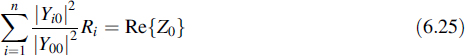
Passive networks are reciprocal, so that Yi0 = Y0i. Substituting this into Equation (6.25) and the result from Equation (6.21) yields the following theorem.
Theorem 11
If in a passive network comprising several resistors, capacitors, coils and ideal transformers all resistors are at the same temperature T, then the voltage noise spectral density at the open terminals of this network is
![]()
where Z0 is the impedance of the network at the open terminal pair.
This generalization of Equation (6.6) is called Nyquist's theorem. Comparing Equation (6.26) with Equation (6.17) and if we take Te = T, then the equivalent noise resistance becomes equal to Re{Z0}. When defining this quantity we emphasized that it can be frequency dependent. This is further elucidated when studying Example 6.1, which is presented in Figure 6.3.
Example 6.2:
Let us reconsider the problem presented in Example 6.1. The impedance at the terminals of Figure 6.3(a) reads
![]()
with its real part
![]()
Substituting this expression into Equation (6.26) produces the voltage spectral density at the terminals
![]()
As expected, this is equal to the expression of Equation (6.11).
![]()
Equation (6.26) is a description according to Thévenin's equivalent circuit model (see Figure 6.1). A description in terms of Norton's equivalent circuit model is possible as well (see Figure 6.2). Then
![]()
where
![]()
Equation (6.30) presents the spectrum of the current that will flow through the shortcut that is applied to a certain terminal pair of a network. Here Y0 is the admittance of the network at the shortcut terminal pair.
6.4 SYSTEM NOISE
The method presented in the preceding section can be applied to all noisy components in amplifiers and other subsystems that constitute a system. However, this leads to very extensive and complicated calculations and therefore is of limited value. Moreover, when buying a system the required details for such an analysis are not available as a rule. There is therefore a need for an alternative more generic noise description for (sub)systems in terms of relations between the input and output. Based on this, the quality of components, such as amplifiers, can be characterized in terms of their own noise contribution. In this way the noise behaviour of a system can be calculated simply and quickly.
6.4.1 Noise in Amplifiers
In general, amplifiers will contribute considerably to noise in a system, owing to the presence of noisy passive and active components in it. In addition, the input signals of amplifiers will in many cases also be disturbed by noise. We will start our analysis by considering ideal, i.e. noise-free, amplifiers. The most general equivalent scheme is presented in Figure 6.6. For the sake of simplifying the equations we will assume that all impedances in the scheme are real. A generalization to include reactive components is found in reference [4]. The amplifier has an input impedance of Ri, an output impedance of Ro and a transfer function of H(ω). The source has an impedance of Rs and generates as open voltage a wide-sense stationary stochastic voltage process Vs with the spectral density Sss(ω). This process may represent noise or an information signal, or a combination (addition) of these types of processes. The available spectral density of this source is Ss(ω) = Sss(ω)/(4Rs). This follows from Equation (6.15) where the two resistances are set at the same value Rs. Using Equation (4.27), the available spectral density at the output of the amplifier is found to be

The available power gain of the amplifier is defined as the ratio of the available spectral densities of the sources from Figure 6.6:

In case the impedances at the input and output are matched to produce maximum power transfer (i.e. Ri = Rs and Ro = RL), the practically measured gain will be equal to the available gain.
Now we will assume that the input source generates white noise, either from a thermal noise source or not, with an equivalent noise temperature of Ts. Then Ss(ω) = kTs/2 and the available spectral density at the output of the amplifier, supposed to be noise free, may be written as
![]()

Figure 6.6 Model of an ideal (noise-free) amplifier with noise input

Figure 6.7 Block schematic of a noisy amplifier with the amplifier noise positioned (a) at the output or (b) at the input
From now on we will assume that the amplifier itself produces noise as well and it seems to be reasonable to suppose that the amplifier noise is independent of the noise generated by the source Vs. Therefore the available output spectral density is
![]()
where Sint(ω) is the available spectral density at the output of the amplifier as a consequence of the noise produced by the internal noise sources present in the amplifier itself. The model that corresponds to this latter expression is drawn in Figure 6.7(a). The total available noise power at the output is found by integrating the output spectral density
![]()
This output noise power will be expressed in terms of the equivalent noise bandwidth (see Equation (4.51)) for the sake of simplifying the notation. For ω0 we substitute that value for which the gain is maximal and we denote at that value Ga(ω0) = G. Then it is found that
![]()
Using this latter equation the first term of the right-hand side of Equation (6.36) can be written as GkTsWN/(2π). In order to be able to write the second term of that equation in a similar way the effective noise temperature of the amplifier is defined as
![]()
Based on this latter equation the total noise power at the output is written as
![]()
It is emphasized that WN/(2π) represents the equivalent noise bandwidth in hertz. By the representation of Equation (6.39) the amplifier noise is in the model transferred to the input (see Figure 6.7(b)). In this way it can immediately be compared with the noise generated by the source at the input, which is represented by the first term in Equation (6.39).
6.4.2 The Noise Figure
Let us now consider a noisy device, an amplifier or a passive device, and let us suppose that the device is driven by a source that is noisy as well. The noise figure F of the device is defined as the ratio of the total available output noise spectral density (due to both the source and device) and the contribution to that from the source alone, in the later case supposing that the device is noise free. In general, the two noise contributions can have frequency-dependent spectral densities and thus the noise figure can also be frequency dependent. In that case it is called the spot noise figure. Another definition of the noise figure can be based on the ratio of the two total noise powers. In that case the corresponding noise figure is called the average noise figure. In many situations, however, the noise sources can be modelled as white sources. Then, based on the definition and Equation (6.39), it is found that
![]()
It will be clear that different devices can have different effective noise temperatures; this depends on the noise produced by the device. However, suppliers want to specify the quality of their devices for a standard situation. Therefore the standard noise figure for the situation where the source is at room temperature is defined as
![]()
Thus for a very noisy device the effective noise temperature is much higher than room temperature (Te ![]() T0) and Fs
T0) and Fs ![]() 1. This does not mean that the physical temperature of the device is very high; this can and will, in general, be room temperature as well.
1. This does not mean that the physical temperature of the device is very high; this can and will, in general, be room temperature as well.
Especially for amplifiers, the noise figure can also be expressed in terms of signal-to-noise ratios. For that purpose the available signal power of the source is denoted by Ps, so that the signal-to-noise ratio at the input reads
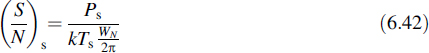
Note that the input noise power has only been integrated over the equivalent noise bandwidth WN of the amplifier, although the input noise power is actually unlimited. This procedure is followed in order to be able to compare the input and output noise power based on the same bandwidth; for the output noise power it does not make any difference. It is an obvious choice to take for this bandwidth, the equivalent noise bandwidth, as this will reflect the actual noise power at the output. Furthermore, it is assumed that the signal spectrum is limited to the same bandwidth, so that the available signal power at the output is denoted as Pso = GPs. Using Equation (6.39) we find that the signal-to-noise ratio at the output is
This signal-to-noise ratio is related to the signal-to-noise ratio at the input as

As the first factor in this expression is always smaller than 1, the signal-to-noise ratio is always deteriorated by the amplifier, which may not surprise us. This deterioration depends on the value of the effective noise temperature compared to the equivalent noise temperature of the source. If, for example, Te ![]() Ts, then the signal-to-noise ratio will hardly be reduced and the amplifier behaves virtually as a noise-free component. From Equation (6.44), it follows that
Ts, then the signal-to-noise ratio will hardly be reduced and the amplifier behaves virtually as a noise-free component. From Equation (6.44), it follows that

Note that the standard noise figure is defined for a situation where the source is at room temperature. This should be kept in mind when determining F by means of a measurement. Suppliers of amplifiers provide the standard noise figure as a rule in their data sheets, mostly presented in decibels (dB).
Sometimes, the noise figure is defined as the ratio of the two signal-to-noise ratios given in Equation (6.45). This can be done for amplifiers but can cause problems when considering a cascade of passive devices such as attenuators, since in that case input and output are not isolated and the load impedance of the source device is also determined by the load impedance of the devices.
Example 6.3:
As an interesting and important example, we investigate the noise figure of a passive two-port device such as a cable or an attenuator. Since the two-port device is passive it is reasonable to suppose that the power gain is smaller than 1 and denoted as G = 1/L, where L is the power loss of the two-port device. The signal-to-noise ratio at the input is written as in Equation (6.42), while the output signal power is by definition Pso = Ps/L. The passive two-port device is assumed to be at temperature Ta. The available spectral density of the output noise due to the noise contribution of the two-port device itself is determined by the impedance of the output terminals, according to Theorem 11. This spectral density is kTa/2. The contribution of the source to the output available spectral density is kTs/(2L). However, since the resistance Rs of the input circuit is part of the impedance that is observed at the output terminals, the portion kTa/(2L) of its noise contribution to the output is already involved in the noise kTa/2, which follows from the theorem. Only compensation for the difference in temperature is needed; i.e. we have to include an extra portion k(Ts − Ta)/(2L).
Now the output signal-to-noise ratio becomes
After some simple calculations the noise figure follows from the definition
![]()
When the two-port device is at room temperature this expression reduces to
![]()
It is therefore concluded that the noise figure of a passive two-port device equals its power loss.
![]()
6.4.3 Noise in Cascaded Systems
In this subsection we consider the cascade connection of systems that may comprise several noisy amplifiers and other noisy components. We look for the noise properties of such a cascade connection, expressed as the parameters of the individual components as they are developed in the preceding subsection. In order to guarantee that the maximum power transfer occurs from one device to another, we assume that the impedances are matched; i.e. the input impedance of a device is the complex conjugate (see Problem 6.7) of the output impedance of the driving device. For the time being and for the sake of better understanding we only consider here a simple configuration consisting of the cascade of two systems (see Figure 6.8). The generalization to a cascade of more than two systems is quite simple, as will be shown later on. In the figure the relevant quantities of the two systems are indicated; they are the maximum power gain Gi, the effective noise temperature Tei and the equivalent noise bandwidth Wi. The subscripts i refer to system 1 for i = 1 and to system 2 for i = 2, while the noise first enters system 1 and the output of system 1 is connected to the input of system 2 (see Figure 6.8). We assume that the passband of system 2 is completely encompassed by that of system 1, and as a consequence W2 ≤ W1. This condition guarantees that all systems contribute to the output noise via the same bandwidth. Therefore, the equivalent noise bandwidth is equal to that of system 2:
![]()

Figure 6.8 Cascade connection of two noisy two-port devices
The gain of the cascade is described by the product
![]()
The total output noise consists of three contributions: the noise of the source that is amplified by both systems, the internal noise produced by system 1 and which is amplified by system 2 and the internal noise of system 2. Therefore, the output noise power is
![]()
where the temperature expression
![]()
is called the system noise temperature. From this it follows that the effective noise temperature of the cascade of the two-port devices in Figure 6.8 (see Equation (6.39)) is
![]()
and the noise figure of the cascade is found by inserting this equation into Equation (6.41), to yield
![]()
Repeated application of the given method yields the effective noise temperature
![]()
and from that the noise figure of a cascade of three or more systems is
![]()
These two equations are known as the Friis formulas. From these formulas it is concluded that in a cascade connection the first stage plays a crucial role with respect to the noise behaviour; namely the noise from this first stage fully contributes to the output noise, whereas the noise from the next stages is to be reduced by a factor equal to the gain that precedes these stages. Therefore, in designing a system consisting of a cascade, the first stage needs special attention; this stage should show a noise figure that is as low as possible and a gain that is as large as possible. When the gain of the first stage is large, the effective noise temperature and noise figure of the cascade are virtually determined by those of the first stage. Following stages can provide further gain and eventual filtering, but will hardly influence the noise performance of the cascade. This means that the design demands of these stages can be relaxed.
Suppose that the first stage is a passive two-port device (e.g. a connection cable) with loss L1. Inserting G1 = 1/L1 into Equation (6.56) yields

Such a situation always causes the signal-to-noise ratio to deteriorate severely as the noise figure of the cascade consists mainly of that of the second (amplifier) stage multiplied by the loss of the passive first stage. When the second stage is a low-noise amplifier, this amplifier cannot repair the deterioration introduced by the passive two-port device of the first stage. Therefore, in case a lossy cable is needed to connect a low-noise device to processing equipment, the source first has to be amplified by a low-noise amplifier before applying it to the connection cable. This is elucidated by the next example.
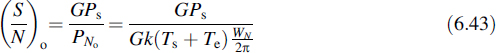
Example 6.4:
Consider a satellite antenna that is connected to a receiver by means of a coaxial cable and an amplifier. The connection scheme and data of the different components are given in Figure 6.9. The antenna noise is determined by the low effective noise temperature of the dark sky (30 K) and produces an information signal power of −90 dBm in a bandwidth of 1 MHz at the input of the cable, which is at room temperature. All impedances are such that all the time maximum power transfer occurs. The receiver needs at least a signal-to-noise ratio of 17 dB. The question is whether the cascade can meet this requirement.
The signal power at the input of the receiver is
![]()
Using Equation (6.51), the noise power at the input of the receiver is
![]()
Figure 6.9 Satellite receiving circuit
On the linear scale, Gampl = 106 and Gcoax = 0.63. The effective noise temperatures of the coax and amplifier, according to Equation (6.41), are

Inserting the numerical data into Equation (6.59) yields
![]()
The ratio of Psr and PN0 produces the signal-to-noise ratio

It is concluded that the cascade satisfies the requirement of a minimum signal-to-noise ratio of 17 dB.
![]()
Although the suppliers characterize the components by the noise figure, in calculations as given in this example it is often more convenient to work with the effective noise temperatures in the way shown. Equation (6.41) gives a simple relation between the two data.
From the example it is clear that the coaxial cable does indeed cause the noise of the amplifier to be dominant.
Example 6.5:
As a second example of the noise figure of cascaded systems, we consider two different optical amplifiers, namely the so-called Erbium-doped fibre amplifier (EDFA) and the semiconductor optical amplifier (SOA). The first type is actually a fibre and so the insertion in a fibre link will give small coupling losses, let us say 0.5 dB. The second type, being a semiconductor device, has smaller waveguide dimensions than that of a fibre, which causes relatively high loss, let us say a 3 dB coupling loss. From physical reasoning it follows that optical amplifiers have a minimum noise figure of 3 dB. Let us compare the noise figure when either amplifier is inserted in a fibre link, where each of them has an amplification of 30 dB. On insertion we can distinguish three stages: (1) the coupling from the transmission fibre to the amplifier, (2) the amplifier device itself (EDFA or SOA) and (3) the output coupling from the amplifier device to the fibre. Using Equation (6.57) and the given data of these stages, the noise figure and other relevant data of the insertion are summarized in Table 6.1; note that in this table all data are in dB (see Appendix B). It follows from these data that the noise figure on insertion of the SOA is approximately 2.5 dB worse than that of the EDFA. This is almost completely attributed to the higher coupling loss at the front end of the amplifier. The output coupling hardly influences this number; it only contributes to a lower net gain.
![]()
Table 6.1 Comparing different optical amplifiers

These two examples clearly show that in a cascade it is of the utmost importance that the first component (the front end) consists of a low-noise amplifier with a high gain, so that the front end contributes little noise and reduces the noise contribution of the other components in the cascade.
6.5 SUMMARY
A stochastic process is called ‘white noise’ if its power spectral density has a constant value for all frequencies. From a physical point of view this is impossible; namely this would imply an infinitely large amount of power. The concept in the first instance is therefore only of mathematical and theoretical value and may probably be used as a model in a limited but practically very wide frequency range. This holds specifically for thermal noise that is produced in resistors. In order to analyse thermal noise in networks and systems, we introduced the Thévenin and Norton equivalent circuit models. They consist of an ideal, that is noise-free, resistor in series with a voltage source or in parallel with a current source. Then, using network theoretical methods and the results from Chapter 4, the noise at the output of the network can easily be described. Several resistors in a network are considered as independent noise sources, where the superposition principle may be applied. Therefore, the total output power spectral density consists of the sum of the output spectra due to the individual resistors.
Calculating the noise behaviour of systems based on all the noisy components requires detailed data of the constituting components. This leads to lengthy calculations and frequently the detailed data are not available. A way out is offered by noise characterization of (sub)systems based on their output data. These output noise data are usually provided by component suppliers. Important data in this respect are the effective noise temperature and/or the noise figure. On the basis of these parameters, the influence of the subsystems on the noise performance of a cascade can be calculated. From such an analysis it appears that the first stage of a cascade plays a crucial role. This stage should contribute as little as possible to the output noise (i.e. it must have a low effective noise temperature or, equivalently, a low-noise figure) and a high gain. The use of cables and attenuators as a first stage has to be avoided as they strongly deteriorate the signal-to-noise ratio. Such components should be preceded by low-noise amplifiers with a high gain.
6.6 PROBLEMS
6.1 Consider the thermal noise spectrum given by Equation (6.3).
(a) For which frequency range will this given spectrum have a value larger than 0.9 × 2kTR at room temperature?
(b) Use Matlab to plot this power spectral density as a function of frequency, for R = 1 Ω at room temperature.
(c) What is the significance of thermal noise in the optical domain, if it is realized that the optical domain as it is used for optical communication runs to a maximum wavelength of 1650 nm?
6.2 A resistance R1 is at absolute temperature T1 and a second resistance R2 is at absolute temperature T2.
(a) What is the equivalent noise temperature of the series connection of these two resistances?
(b) If T1 = T2 = T what in that case is the value of Te?
6.3 Answer the same questions as in Problem 6.2 but now for the parallel connection of the two resistances.
6.4 Consider once more the circuit of Problem 6.2. A capacitor with capacitance C1 is connected parallel to R1 and a capacitor with capacitance C2 is connected parallel to R2.
(a) Calculate the equivalent noise temperature.
(b) Is it possible to select the capacitances such that Te becomes independent of frequency?
6.5 A resistor with a resistance value of R is at temperature T kelvin. A coil is connected parallel to this resistor with a self-inductance L henry. Calculate the mean value of the energy that is stored in the coil as a consequence of thermal noise produced by the resistor.
6.6 An electrical circuit consists of a loop of three elements in series, two resistors and a capacitor. The capacitance is C farad and the resistances are R1 and R2 respectively. Resistance R1 is at temperature T1 K and resistance R2 is at T2 K. Calculate the mean energy stored in the capacitor as a consequence of the thermal noise produced by the resistors.
6.7 A thermal noise source has an internal impedance of Z(ω). The noise source is loaded by the load impedance Z1(ω).
(a) Show that a maximum power transfer from the noise source to the load occurs if Z1 = Z*(ω).
(b) In that case what is the available power spectral density?
6.8 A resistor with resistance R1 is at absolute temperature T1. A second resistor with resistance R2 is at absolute temperature T2. The resistors R1 and R2 are connected in parallel.
(a) What is the spectral density of the net amount of power that is exchanged between the two resistors?
(b) Does the colder of the two resistors tend to further cool down due to this effect or heat up? In other words does the system strive for temperature equalization or does it strive to increase the temperature differences?
(c) What is the power exchange if the two temperatures are of equal value?


6.9 Consider the circuit in Figure 6.10, where all components are at the same temperature.
(a) The thermal noise produced by the resistors becomes manifest at the terminals. Suppose that the values of the components are such that the noise spectrum at the terminals is white. Derive the conditions in order for this to happen.
(b) What is in that case the impedance at the terminals?
6.10 Consider the circuit presented in Figure 6.11. The input impedance of the amplifier is infinitely high.
(a) Derive the expression for the spectral density SVV(ω of the input voltage V(t) of the amplifier as a consequence of the thermal noise in the resistance R.
The lowpass filter H(ω) is ideal, i.e.
![]()
In the passband of H(ω) the constant τ = 1 and the voltage amplification A can also be taken as constant and equal to 103. The amplifier does not produce any noise. The component values of the input circuit are C = 200 nF and R = 1 kΩ. The resistor is at room temperature so that kT = 4 × 10⁻²¹ W s.
(b) Calculate the r.m.s. value of the output voltage Vo(t) of the filter in the case W = 1/(RC).
6.11 Consider the circuit given in Figure 6.12. The data are as follows: R = 50 Ω, L = 1 μH, C = 400 pF and A = 100.
(a) Calculate the spectral density of the noise voltage at the input of the amplifier as a consequence of the thermal noise produced by the resistors. Assume that these resistors are at room temperature and the other components are noise free.
(b) Calculate the transfer function H(ω) from the output amplifier to the input filter.
(c) Calculate the spectral density of the noise voltage at the input of the filter.
(d) Calculate the r.m.s. value of the noise voltage at the filter output in the case where the filter is ideal lowpass with a transfer of 1 and a cut-off angular frequency ωc = π/TD, where TD = 10 ns.
6.12 A signal source has a source impedance of 50 Ω and an equivalent noise temperature of 3000 K. This source is terminated by the input impedance of an amplifier, which is also 50 Ω. The voltage across this resistor is amplified and the amplifier itself is noise free. The voltage transfer function of the amplifier is
![]()
where τ = 10−8 s. The amplifier is at room temperature. Calculate the variance of the noise voltage at the output of the amplifier.
6.13 An amplifier is constituted from three stages with effective noise temperatures of Te1 = 1300 K, Te2 = 1750 K and Te3 = 2500 K, respectively, and where stage number 1 is the input stage, etc. The power gains amount to G1 = 20, G2 = 10 and G3 = 5, respectively.
(a) Calculate the effective noise temperature of this cascade of amplifier stages.
(b) Explain why this temperature is considerably lower than Te2, respectively Te3.
6.14 An antenna has an impedance of 300 Ω. The antenna signal is amplified by an amplifier with an input impedance of 50 Ω. In order to match the antenna to the amplifier input impedance a resistor with a resistance of 300 Ω is connected in series with the antenna and parallel to the amplifier input a resistance of 50 Ω is connected.
(a) Sketch a block schematic of antenna, matching network and amplifier.
(b) Calculate the standard noise figure of the matching network.
(c) Do the resistances of 300 and 50 Ω provide matching of the antenna and amplifier? Support your answer by a calculation.
(d) Design a network that provides all the matching functionalities.
(e) What is the standard noise figure of this latter network? Compare this with the answer found for question (b).
6.15 An antenna is on top of a tall tower and is connected to a receiver at the foot of the tower by means of a cable. However, before applying the signal to the cable it is amplified. The amplifier has a power gain of 20 dB and a noise figure of F = 3 dB. The cable has a loss of 6 dB, while the noise figure of the receiver amounts to 13 dB. All impedances are matched; i.e. between components the maximum power transfer occurs.
(a) Calculate the noise figure of the system.
(b) Calculate the noise figure of the modified system where the amplifier is placed between the cable and the receiver at the foot of the tower instead of between the antenna and the cable at the top of the tower.
6.16 Reconsider Example 6.4. Interchange the order of the coaxial cable and the amplifier. Calculate the signal-to-noise ratio at the input of the receiver for this new situation.
6.17 An antenna is connected to a receiver via an amplifier and a cable. For proper operation the receiver needs at its input a signal-to-noise ratio of at least 20 dB. The amplifier is directly connected to the antenna and the cable connects the amplifier (power amplification of 60 dB) to the receiver. The cable has a loss of 1 dB and is at room temperature (290 K). The effective noise temperature of the antenna amounts to 50 K. The received signal is −90 dBm at the input of the amplifier and has a bandwidth of 10 MHz. All impedances are such that the maximum power transfer occurs.
(a) Present a block schematic of the total system and indicate in that sketch the relevant parameters.
(b) Calculate the signal power at the input of the receiver.
(c) The system designer can select one out of two suppliers for the amplifier. The suppliers A and B present the data given in Table 6.2. Which of the two amplifiers can be used in the system, i.e. on insertion of the amplifiers in the system which one will meet the requirement for the signal-to-noise ratio? Support your answer with a calculation.
6.18 Consider a source with a real source impedance of Rs. There are two passive networks as given in Figure 6.13. Resistance R1 is at temperature T1 K and resistance R2 is at temperature T2 K.
(a) Calculate the available power gain and standard noise factor when the circuit comprising R1 is connected to the source.
(b) Calculate the available power gain and standard noise factor when the circuit comprising R2 is connected to the source.


(c) Now assume that the two networks are cascaded where R1 is connected to the source and R2 to the output. Calculate the available gain and the standard noise figure of the cascade when connected to this source.
(d) Do the gains and the noise figures satisfy Equations (6.50) and (6.54), respectively? Explain your conclusion.
(e) Redo the calculations of the gain and noise figure when Rs + R1 is taken as the source impedance for the second two-port device, i.e. the impedance of the source and the first two-port device as seen from the viewpoint of the second two-port device.
(f) Do the gains and the noise figures in case (e) satisfy Equations (6.50) and (6.54), respectively?
6.19 Consider a source with a complex source impedance of Zs. This source is loaded by the passive network given in Figure 6.14.
(a) Calculate the available power gain and noise factor of the two-port device when it is connected to the source.
(b) Do the answers from (a) surprise you? If the answer is ‘yes’ explain why. If the answer is ‘no’ explain why not.
6.20 Consider the circuit given in Figure 6.15. This is a so-called ‘constant resistance network’.
(a) Show that the input impedance of this circuit equals R0 if ![]() and the circuit is terminated by a resistance R0.
and the circuit is terminated by a resistance R0.
(b) Calculate the available power gain and noise figure of the circuit (at temperature T kelvin) if the source impedance equals R0 (which is at temperature Ts kelvin).
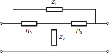
(c) Suppose that two of these circuits at different temperatures and with different gains are put in cascade and that the source impedance equals R0 once more (also at temperature Ts kelvin). Calculate the overall available power gain and noise figure.
(d) Does the overall gain equal the product of the gains?
(e) Under what circumstances does the noise figure obey Equation (6.54)?
Introduction to Random Signals and Noise W. van Etten
© 2005 John Wiley & Sons, Ltd