
Chapter 14 Conductors, insulators and dielectrics
- 14.1 Introduction and synopsis 308
- 14.2 Conductors, insulators and dielectrics 309
- 14.3 Charts for electrical properties 314
- 14.4 Drilling down: the origins and manipulation of electrical properties 316
- 14.5 Design: using the electrical properties of materials 328
- 14.6 Summary and conclusions 334
- 14.7 Further reading 335
- 14.8 Exercises 335
- 14.9 Exploring design with CES 337
- 14.10 Exploring the science with CES Elements 339
York Minster, constructed between 1220 and 1400, is one of the great cathedrals of Europe. Many fine sermons have been preached from its pulpit, but in 1984, when the Archbishop of York expressed his disbelief in the Virgin Birth, the Minster was struck by lightning and severely damaged. Some put this down to the wrath of God, but the reality is simpler: the cathedral was inadequately earthed. There is a message here: even when you are designing cathedrals, electrical properties matter.
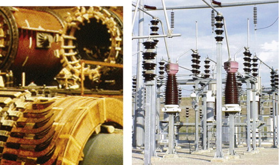
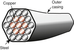
Conductors and insulators. Copper, aluminum and silver (if you can afford it) make good conductors. Pyrex, porcelain and ceramics like alumina make good insulators—they are dielectrics.
(Images courtesy of the Copper Development Association)
14.1 Introduction and synopsis
York Minster, constructed between 1220 and 1400, is one of the great cathedrals of Europe. Many fine sermons have been preached from its pulpit, but in 1984, when the Archbishop of York expressed his disbelief in the Virgin Birth, the Minster was struck by lightning and severely damaged. Some put this down to the wrath of God, but the reality is simpler: the cathedral was inadequately earthed. There is a message here: even when you are designing cathedrals, electrical properties matter.
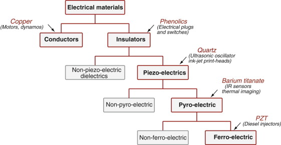
This chapter is about the simplest of these: they relate to conduction, insulation and dielectric behaviour. Electrical conduction (as in lightning conductors) and insulation (as in electric plug casings) are familiar properties. Dielectric behaviour may be less so. A dielectric is an insulator. It is usual to use the word ‘insulator’ when referring to its inability to conduct electricity, and to use ‘dielectric’ when referring to its behaviour in an electric field. Three properties are of importance here. The first, the dielectric constant (or relative permittivity), has to do with the way the material acquires a dipole moment (it polarises) in an electric field. The second, the dielectric loss factor, measures the energy dissipated when radio-frequency waves pass through a material, the energy appearing as heat (the principle of microwave cooking). The third is the dielectric breakdown potential, and this takes us back to York Minster. Lightning is dielectric breakdown, and it can be as damaging on a small scale—in a piece of electrical equipment, for example—as on a large one.
There are many different kinds of electrical behaviour, all of them useful. Figure 14.1 gives an overview, with examples of materials and applications. The chapter introduces electrical properties and their physical origins, and examples of design for electrical performance.
14.2 Conductors, insulators and dielectrics
Resistivity and conductivity
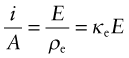
The electrical resistance R (units: ohms1, symbol Ω) of a rod of material is the potential drop V (volts2) across it, divided by the current i (amps3) passing through it, as in Figure 14.2. This relationship is Ohm’s law:
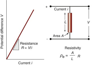

The material property that determines resistance is the electrical resistivity, ρe. It is related to the resistance by

where A is the section and L the length of a test rod of material—think of it as the resistance of a unit cube of the material. Its units in the metric system are Ω.m, but it is commonly reported in units of µΩ.cm. It has an immense range, from a little more than 10−8 in units of Ω.m for good conductors (equivalent to 1 µΩ.cm, which is why these units are still used) to more than 1016Ω.m (1024 µΩ.cm) for the best insulators. The electrical conductivity κe is simply the reciprocal of the resistivity. Its units are siemens per meter S/m or (Ω.m)−1.
Dielectric properties
First, a reminder of what is meant by a field: it is a region of space in which objects experience forces if they have the right properties. Charge creates an electric field, E. The electric field strength between two oppositely charged plates separated by a distance t and with a potential difference V between them is

and is independent of position except near the edge of the plates.
Two conducting plates separated by a dielectric make a capacitor (Figure 14.3). Capacitors (sometimes called condensers) store charge. The charge Q (coulombs4) is directly proportional to the potential difference between the plates, V (volts):
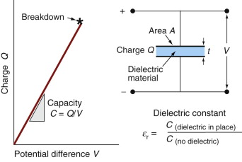
Figure 14.3 Dielectric constant and dielectric breakdown. The capacitance of a condenser is proportional to the dielectric constant, and the maximum charge it can hold is limited by breakdown.
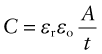
where C (farads5) is the capacitance. The capacitance of a parallel plate capacitor of area A, separated by empty space (or by air), is

where εo is the permittivity of free space (8.85 × 10⁻¹² F/m, where F is farads). If the empty space is replaced by a dielectric, capacitance increases. This is because the dielectric polarises. The field created by the polarisation opposes the field E, reducing the voltage difference V needed to support the charge. Thus, the capacity of the condenser is increased to the new value

where ε is the permittivity of the dielectric, with the same units as εo. It is usual to cite, not this, but the relative permittivity or dielectric constant, εr:
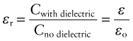
making the capacitance
Being a ratio, εr is dimensionless. Its value for empty space and, for practical purposes, for most gases, is 1. Most dielectrics have values between 2 and 20, though low-density foams approach the value 1 because they are largely air. Ferroelectrics are special: they have values of εr as high as 20 000. More on them later.
Example 14.1
(a) A capacitor has a plate area of A = 0.1 m2 separated by an air gap of t = 100 µm. What is its capacitance? (b) The air gap is replaced by a dielectric of thickness t = 1 µm with a dielectric constant εr = 20. What is its capacitance now?
Capacitance is one way to measure the dielectric constant of a material (Figure 14.3). The charge stored in the capacitor is measured by integrating the current that flows into it as the potential difference V is increased. The ratio Q/V is the capacitance. The dielectric constant εr is calculated from equation (14.7).
Small capacitors, with capacitances measured in microfarads (µF) or picofarads (pF), are used in R–C circuits to tune oscillations and give controlled time delays. The time constant for charging or discharging a capacitor in series with a resistor is
where R is the resistance of the circuit. When charged, the energy stored in a capacitor is
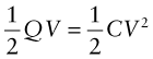
and this can be large: ‘super-capacitors’ with capacitances measured in farads store enough energy to power a hybrid car.
The breakdown potential or dielectric strength (units: MV/m) is the electrical potential gradient at which an insulator breaks down and a damaging surge of current flows through it. It is measured by increasing, at a uniform rate, a 60 Hz alternating potential applied across the faces of a plate of the material in a configuration like that of Figure 14.3 until breakdown occurs, typically at a potential gradient of between 1 and 100 MV/m.
Example 14.2
A supercapacitor is required that is able to store an energy of E = 1 kJ when a potential difference V = 100 volts is applied to its plates. The dielectric constant of the dielectric is εr = 10 000 and its breakdown potential is B = 2 × 10⁷ V/m. What is the minimum area of plate required?
Answer. Breakdown occurs if ![]() , requiring a dielectric thickness t ≥ 5 µm. Theenergy stored in a capacitor is
, requiring a dielectric thickness t ≥ 5 µm. Theenergy stored in a capacitor is ![]() , so a capacitance of
, so a capacitance of ![]() isneeded. To achieve this with a dielectric of thickness t ≥ 5 µm and dielectric constant10 000 requires and area
isneeded. To achieve this with a dielectric of thickness t ≥ 5 µm and dielectric constant10 000 requires and area ![]() .
.
The loss tangent and the loss factor take a little more explanation. We shall see in Section 14.4 that polarisation involves the small displacement of charge (either of electrons or of ions) or of molecules that carry a dipole moment when an electric field is applied to the material. An oscillating field drives the charge between two alternative configurations. This charge motion is like an electric current that—if there were no losses—would be 90° out of phase with the voltage. In real dielectrics this current dissipates energy, just as a current in a resistor does, giving it a small phase shift, δ (Figure 14.4). The loss tangent, tan δ, also called the dissipation factor, D, is the tangent of the loss angle. The power factor, Pf, is the sine of the loss angle. When δ is small, as it is for the materials of interest here, all three are essentially equivalent:
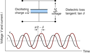
Figure 14.4 Dielectric loss. The greater the loss factor, the greater is the microwave coupling and heating.
More useful, for our purposes, is the loss factor L, which is the loss tangent times the dielectric constant:
It measures the energy dissipated in a dielectric when in an oscillating field. If you want to select materials to minimise or maximise dielectric loss, then the measure you want is L.
When a dielectric material is placed in a cyclic electric field of amplitude E and frequency f, power P is dissipated and the field is correspondingly attenuated. The power dissipated per unit volume, in W/m3, is
where, as before, εr is the dielectric constant of the material and tan δ is its loss tangent. This power appears as heat and is generated uniformly through the volume of the material. Thus, the higher the frequency or the field strength and the greater the loss factor εr tan δ, the greater is the heating and energy loss. This dielectric loss is exploited in processing—for example, in radio-frequency welding of polymers.
All dielectrics change shape in an electric field, a consequence of the small shift in charge that allows them to polarise; the effect is called electrostriction. Electrostriction is a one-sided relationship in that an electric field causes deformation, but deformation does not produce an electric field. Piezo-electric materials, by contrast, display a two-sided relationship between polarisation and deformation: a field induces deformation and deformation induces charge differences between its surfaces, thus creating a field. The piezo-electric coefficient is the strain per unit of electric field, and although it is very small, it is a true linear effect, and this makes it useful: when you want to position or move a probe with nanoscale precision it is just what you need. Pyro-electric materials contain molecules with permanent dipole moments that, in a single crystal, are aligned, giving the crystal a permanent polarisation. When the temperature is changed the polarisation changes, creating surface charges or, if the surfaces are connected electrically, a pyro-electric current—the principle of intruder detection systems and of thermal imaging. Ferro-electric materials, too, have a natural dipole moment—they are polarised to start with, and the individual polarised molecules line up so that their dipole moments are parallel, like magnetic moments in a magnet. Their special feature is that the direction of polarisation can be changed by applying an electric field, and the change causes a change of shape. Applications of all of these are described in Section 14.5.
Example 14.3
(a) An oscillating voltage with an amplitude of 100 volts at a frequency f = 60 Hz appears across a nylon insulator thickness x = 1 mm. Nylon has a dielectric loss factor L ≈ 0.1. How much power is dissipated per unit volume in the nylon? Assuming no heat loss, how fast will the temperature of the nylon rise? (Nylon has a volumetric specific heat Cp = 3 × 10⁶ J/m3.K.) (b) If the frequency was, instead, f = 1 GHz, what is the heating rate?
14.3 Charts for electrical properties
All materials have an electrical resistivity and all dielectrics have a dielectric constant and loss factor. Property charts for these are useful because they allow comparison and selection from a large and varied population. Certain other properties are peculiar to only a handful of materials: useful piezo-electric and ferro-electric behaviour are examples. Selection is then a case of a choice between a small number of candidates, easily explored by direct comparison. Property charts for these are not necessary.
Thermal conductivity and electrical resistivity
The first chart (Figure 14.5) shows the thermal conductivity λ and the electrical resistivity ρe. The first has a range of 105, the second a range of 1028; no other material property has such a wide range. The chart is useful for selecting materials for applications in which these two properties are important. For metals, thermal and electrical conduction are linked because both depend on free electrons, giving the obvious correlation between the two at the upper left of the chart:
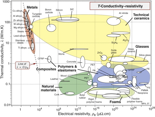

(λ in W/m.K, ρe in µΩ.cm). It is known as the Wiedemann–Franz law.
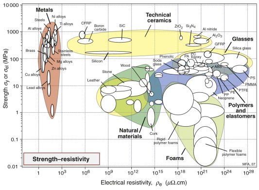
Strength and electrical resistivity
The second chart (Figure 14.6) shows electrical resistivity ρe and strength σel. Metals lie at the extreme left: copper and silver (not shown) have the lowest resistivities, with aluminum only just above. The strongest alloys have resistivities that are 10–100 times larger. Ceramics such as alumina, aluminum nitride and silica, at the upper right, have very high resistivities and are strong; they are used for making insulators for power lines and substrates for electronic circuitry. Below them lie polymers that are less strong, but are flexible, easily moulded and excellent insulators; they are used for cable sheathing, insulation of switch gear and the like.
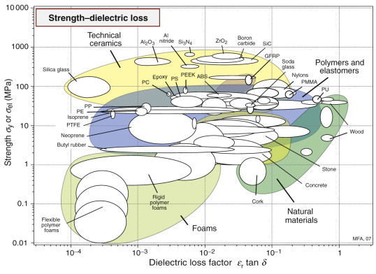
Strength and dielectric loss
The final chart (Figure 14.7) shows dielectric loss factor L and strength σy or σel. Materials that are transparent to microwaves (radar uses microwave frequencies) lie at the left: polymer foams, certain polymers (PP, PE, PTFE) and some ceramics have particularly low values. Materials that absorb microwaves, becoming hot in the process, lie at the right: polymers containing a polar group, like nylon and polyurethane, and natural materials like woods (woods are dried by microwave heating). Water, which has a polar molecule, has a particularly large loss factor, which is why most foods can be cooked in a microwave oven.
14.4 Drilling down: the origins and manipulation of electrical properties
Electrical conductivity
An electric field, E (volts/m), exerts a force Ee on a particle carrying a charge. Solids are made up of atoms containing electrons that carry a charge −e and a nucleus containing protons, each with a positive charge +e. If charge carriers can move, the force Ee causes them to flow through the material—that is, it conducts. Metals are electron conductors, meaning that the charge carriers are the electrons. In ionic solids (which are composed of negatively and positively charged ions like Na+ Cl−) the diffusive motion of ions allows ionic conduction, but this is only possible at temperatures at which diffusion is rapid. Many materials have no mobile electrons, and at room temperature they are too cold to be ionic conductors. The charged particles they contain still feel a force in an electric field and it is enough to displace the charges slightly, but they are unable to move more than a tiny fraction of the atom spacing. These are insulators; the small displacement of charge gives them dielectric properties.
How is it that some materials have mobile electrons and some do not? To explain this we need two of the stranger results of quantum mechanics. Briefly, the electrons of an atom occupy discrete energy states or orbits, arranged in shells (designated 1, 2, 3, etc. from the innermost to the outermost); each shell is made up of sub-shells (designated s, p, d and f), each of which contains one, three, five or seven orbits, respectively. The electrons fill the shells with the lowest energy, two electrons of opposite spin in each orbit; the Pauli6 exclusion principle prohibits an energy state with more than two. When n atoms (a large number) are brought together to form a solid, the inner electrons remain the property of the atom on which they started, but the outer ones interact (Figure 14.8). Each atom now sits in the field created by the charges of its neighbors. This has the effect of decreasing slightly the energy levels of electrons spinning in a direction favored by the field of its neighbors and raising that of those with spins in the opposite direction, splitting each energy level. Thus, the discrete levels of an isolated atom broaden, in the solid, into bands of very closely spaced levels. The number of electrons per atom that have to be accommodated depends only on the atomic number of the atoms. These electrons fill the bands from the bottom, lowest energy, slot on up, until all are on board, so to speak. The topmost filled energy level is called the Fermi7 level (more on this later). An electron in this level still has an energy that is lower than it would have if it were isolated in a vacuum far from the atoms. This energy difference is called, for historical reasons, the work function because it is the work that you have to do to remove an electron from the Fermi level to infinity. If you want to create an electron beam by pulling electrons out of a metal by using a high electric field (called a field-emission electron gun) you have to provide the work function to do it.
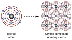
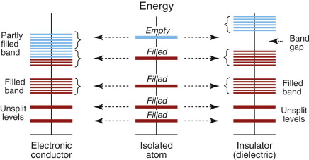
Figure 14.8 When atoms are brought together to form crystals, the outermost electrons interact and the discrete energy levels split into bands.
Whether the material is a conductor or an insulator depends on how full the bands are, and whether or not they overlap. In Figure 14.9 the central column describes an isolated atom and the outer ones illustrate the possibilities created by bringing atoms together into an array, with the energies spread into energy bands. Conductors like copper, shown on the left, have an unfilled outer band; there are many very closely spaced levels just above the last full one, and—when accelerated by a field—electrons can use these levels to move freely through the material. In insulators, shown on the right, the outermost band with electrons in it is full, and the nearest empty band is separated from it in energy by a wide band gap. Semiconductors, too, have a band gap, but it is narrower—narrow enough that thermal energy can pop a few electrons into the empty band, where they conduct. Deliberate doping (adding trace levels of impurities) creates new levels in the band gap, reducing the energy barrier to entering the empty states and thus allowing more carriers to become mobile.
Electrical resistance
If a field E exerts a force Ee on an electron, why does it not accelerate forever, giving a current that continuously increases with time? This is not what happens; instead, switching on a field causes a current that almost immediately reaches a steady value. Referring back to equations (14.1) and (14.2), the current density i/A is proportional to the field E:
where ρe is the resistivity and κe, its reciprocal, is the electrical conductivity.
Broadly speaking, the picture is this. Conduction electrons are free to move through the solid. Their thermal energy kBT (kB = Boltzmann’s constant, T = absolute temperature) causes them to move like gas atoms in all directions. In doing this they collide with scattering centres, bouncing off in a new direction. Impurity or solute atoms are particularly effective scattering centres (which is why alloys always have a higher resistivity than pure metals), but electrons are scattered also by imperfections such as dislocations and by the thermal vibration of the atoms themselves. When there is no field, there is no net transfer of charge in any direction even though all the conduction electrons are moving freely. A field imposes a drift velocity vd = µeE on the electrons, where µe is the electron mobility and it is this that gives the current (Figure 14.10). The drift velocity is small compared with the thermal velocity; it is like a breeze in air—the thermal motion of the air molecules is far greater than the ‘drift’ that we feel as the breeze. The greater the number of scattering centres, the shorter is the mean free path, λmfp, of the electrons between collisions, and the slower, on average, they move. Just as with thermal conductivity, the electrical conductivity depends on mean free path, on the density of carriers (the number nv of mobile electrons per unit volume) and the charge they carry. Thus, the current density, i/A, is given by
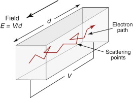
Figure 14.10 An electron, accelerated by the field E, is scattered by imperfections that create a resistance to its motion.
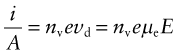
Comparing this with equation (14.14) gives the conductivity:
Thus the conductivity is proportional to the density of free electrons and to the electron mobility, and this is directly proportional to the mean free path. The purer and more perfect the conductor, the higher is the conductivity.
Example 14.4
A conductor-grade copper has a resistivity of ρe = 5 µΩ.cm. Copper is face-centered cubic with a lattice parameter of 0.36 nm. Each copper atom contributes two mobile electrons to the conduction band. What is the mobility of electrons in copper?
Answer. The resistivity of this copper in SI units is 5 × 10⁻⁸ Ω.m. The conductivity κe is the reciprocal of this: κe = 2 × 10⁷ S/m. The charge carried by an electron is e = 1.6 × 10⁻¹⁹ Coulombs (see inside front cover of this book). The volume of the unit cell of copper is
Each unit cell contains two copper atoms, each of which contributes two mobile electrons. Thus the density of mobile electrons is nv = 8.57 × 1028 per m3. Thus the electron mobility is
Metals are strengthened (Chapter 7) by solid solution hardening, work hardening or precipitation hardening. All of these change the resistivity too. By ‘zooming in’ on part of the strength–resistivity chart, we can see how both properties are affected—Figure 14.11 shows this for two of the best conductors: copper and aluminum. Adding solute to either metal introduces scattering centers, increasing the electrical resistivity. Dislocations add strength (by what we called work hardening) and they too scatter electrons a little, though not as much as solute. Precipitates offer the greatest gain in strength; their effect on resistivity varies, depending on their size and spacing compared to the electron mean free path and on the amount of residual solute left in the lattice. Precipitation hardening (with low residual solute) or work hardening is therefore the best way to strengthen conductors. The two figures show that commercial conductor alloys have much greater strength, and only slightly greater resistivity than the pure metals.
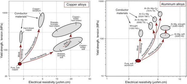
Figure 14.11 The best choice of material for a cable is one with high strength and low resistivity, but strengthening mechanisms increase resistivity. Work hardening and precipitation hardening do so less than solute hardening.
The resistivity of metals increases with temperature because thermal vibration scatters electrons. Resistance decreases as temperature falls, which is why very-high-powered electromagnets are pre-cooled in liquid nitrogen. As absolute zero is approached most metals retain some resistivity, but a few, at between 0 and 4 K, suddenly lose all resistance and become superconducting. The resistivity of semiconductors, by contrast, decreases as temperature increases because, as explained earlier, thermal energy allows more carriers to cross the band gap.
Dielectric behavior
Dielectrics are insulators. So what happens to their electrons when a field E is applied? In zero field, the electrons and protons in most dielectrics are symmetrically distributed, so the material carries no net or dipole moment. A field exerts a force on a charge, pushing positive charges in the direction of the field and negative charges in the opposite direction. The effect is easiest to see in ionic crystals, since here neighbouring ions carry opposite charges, as on the left of Figure 14.12. Switch on the field and the positive ions (charge +q) are pulled in the field direction, the negative ones (charge −q) in the reverse, until the restoring force of the inter-atomic bonds just balances the force due to the field at a displacement of Δx, as on the right of the figure. Two charges ±q separated by a distance Δx create a dipole with dipole moment, d, given by
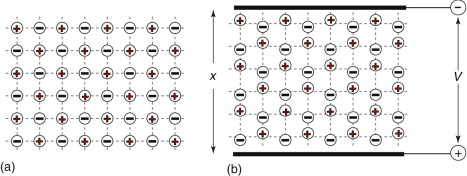
Figure 14.12 An ionic crystal in zero applied field (a), and when a field V/x is applied (b). The electric field displaces charge, causing the material to acquire a dipole moment.
The polarisation of the material, P, is the volume-average of all the dipole moments it contains:
Even in materials that are not ionic, like silicon, a field produces a dipole moment because the nucleus of each atom is displaced a tiny distance in the direction of the field and its surrounding electrons are displaced in the opposite direction. The resulting dipole moment depends on the magnitude of the displacement and the number of charges per unit volume, and it is this that determines the dielectric constant. The bigger the shift, the bigger the dielectric constant. Thus, compounds with ionic bonds and polymers that contain polar groups like —OH− and —NH− (nylon, for example) have larger dielectric constants than those that do not.
Dielectric loss
Think now of polarisation in an alternating electric field. When the upper plate of Figure 14.12(b) is negative, the displacements are in the direction shown in the figure. When its polarity is reversed, it is the negative ions that are displaced upward, the positive ions downward; in an oscillating field, the ions oscillate. If their oscillations were exactly in phase with the field, no energy would be lost, but this is never exactly true, and often the phase shift is considerable. Materials with high dielectric loss usually contain awkwardly shaped molecules that themselves have a dipole moment—the water molecule is an example (Figure 14.13). These respond to the oscillating field by rotating, but because of their shape they interfere with each other (you could think of it as molecular friction) and this dissipates energy that appears as heat—that is how microwave heating works. As equation (14.13) showed, the energy that is dissipated depends on the frequency of the electric field; generally speaking, the higher the frequency, the greater the power dissipated (because power is work per second, and the more times the molecules shuttle, the more energy is lost), but there are peaks at certain frequencies that are characteristic of the material structure.
Example 14.5
An ionic crystal with the rock-salt structure is made up of equal numbers of positive and negative ions each carrying or lacking the charge carried by a single electron. The lattice parameter of the crystal is 0.45 nm. An electric field displaces the ions relative to each other by 1% of the lattice parameter. What is the resulting polarisation?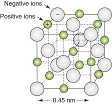
Answer. The dipole moment due to one pair of ions is
The volume of the unit cell is![]() , and each contains two pairs of ions.
, and each contains two pairs of ions.
Dielectric breakdown
In metals, as we have seen, even the smallest field causes electrons to flow. In insulators they can’t, because of the band gap. But if, at some weak spot, one electron is torn free from its parent atom, the force Ee exerted by the field E accelerates it, giving it kinetic energy; it continues to accelerate until it collides with another atom. A sufficiently large field can give the electron so much kinetic energy that, in the collision, it kicks one or more new electrons out of the atom it hits, and they, in turn, are accelerated and gain energy. The result, sketched in Figure 14.14, is a cascade—an avalanche of charge. It is sufficiently violent that it can damage the material permanently.
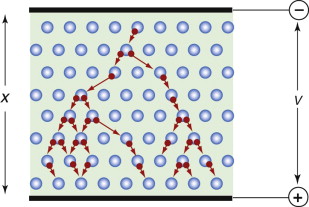
The critical field strength to make this happen, called the breakdown potential, is hard to calculate: it is that at which the first electron breaks free at the weak spot—a defect in the material such as a tiny crack, void or inclusion that locally concentrates the field. The necessary fields are large, typically 1–15 MV/m. That sounds a lot, but such fields are found in two very different circumstances: when the voltage is very high or the distances are very small. In power transmission, the voltages are sufficiently high—20 000 volts or so—that breakdown can occur at the insulators that support the line, whereas in microcircuits and thin-film devices the distances between components are very small: a 1 V difference across a distance of 1 µm gives a field of 1 MV/m.
Piezo-electric materials
The word ‘Quartz’ on the face of your watch carries the assurance that its time-steps are set by the oscillations of a piezo-electric quartz crystal. Piezo-electric behaviour is found in crystals in which the ions are unsymmetrically distributed (the crystal structure lacks a center of symmetry), so that each molecule carries a permanent dipole moment (Figure 14.15(a)). If you cut a little cube from such a material, with faces parallel to crystal planes, the faces would carry charge. This charge attracts ions and charged particles from the atmosphere just as a television screen does, giving an invisible surface layer that neutralises the charge. If you now squeeze the crystal, its ions move relative to each other, the dipole moment changes and the charge on the surface changes too (Figure 14.15(b)). Given time, the newly appeared charge would attract neutralising ions, but this does not happen immediately, giving a potential difference. This provides the basis of operation of electric microphones and pick-ups. The potential difference between the faces can be large—large enough to generate a spark across a narrow gap—it is the way that gas lighters work.
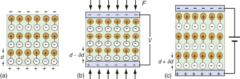
Figure 14.15 A piezo-electric material has unsymmetrically distributed charge, giving it a natural dipole moment. The surface charge associated with this is neutralised by pick-up of ions, but if it is deformed, as in (b), the dipole moment changes and the surfaces become charged. The inverse is also true: a field induces a change of shape, the basis of piezo-electric actuation, as in (c).
A strain, then, induces an electric field in a piezo-electric material. The inverse is also true: a field induces a strain. The field pulls the positive ions and pushes the negative ones, changing their spacing and so changing the shape of the crystal (Figure 14.15(c)). If a small strain produces a large field, then a large field will produce only a very small strain. But the strain is a linear function of field, allowing extremely precise, if small, displacements, used for positioning and actuation at the sub-micron scale.
Piezo-electric materials respond to a change in electric field faster than most materials respond to a stimulus of this or any other kind. Put them in a megahertz field and they respond with microsecond precision. That opens up many applications, some described later in this chapter. In particular, it opens up the world of ultrasonics—sound waves with frequencies starting at the upper limit of the human ear, 20 kHz, up to 20 000 kHz and greater.
Pyro-electric materials
Pyro-electricity—polarisation caused by change of temperature—was known to (but not understood by) the Greek philosopher Theophrastus8, who noted that certain stone, when warmed or cooled, acquired the ability to pick up straw and dry leaves. It was not until the 20th century that this strange behaviour was understood and exploited.
Some materials have a permanent dipole moment because their positive and negative ions balance electrically but are slightly out of line with each other. If a thin disk of one of these is cut so that its faces are parallel to the plane in which the misalignment happens, the disk has a dipole moment of its own. The unit cells of pyro-electric materials are like this. The dipole moment per unit volume of the material is called the spontaneous polarisation Ps. This net dipole moment exists in the absence of an applied electric field and is equivalent to a layer of bound charge on each flat surface. Nearby free charges such as electrons or ions are attracted to the surfaces, neutralising the charge. Imagine that conductive electrodes are then attached to the surfaces and connected through an ampmeter. If the temperature of the sample is constant, then so is Ps and no current flows through the circuit. An increase in temperature, however, causes expansion and that changes the net dipole moment and the polarisation. Redistribution of free charges to compensate for the change in bound charge results in a current flow—the pyro-electric current—in the circuit. Cooling rather than heating reverses the sign of the current. Thus, the pyro-electric current flows only while the temperature is changing—it is the way that intruder alarms, automatic doors and safety lights are activated.
In an open circuit the free charges remain on the electrodes—and that has its uses too, described in the next section. Pyro-electric materials include minerals such as tourmaline (the one Theophrastus found), ceramics such as barium titanate, polymers such as polyvinylidene fluoride and even biological materials, such as collagen.
Ferro-electric materials
Ferro-electrics are a special case of piezo-electric behaviour. They too have an unsymmetric structure, but have the special ability to switch asymmetry. Barium titanate, BaTiO3, shown schematically in Figure 14.16, is one of these. Below a critical temperature, the Curie9 temperature (about 120 °C for barium titanate), the titanium atom, instead of sitting at the centre of the unit cell, is displaced up, down, to the left or to the right, as in (a) and (b). Above the Curie temperature the asymmetry disappears and with it the dipole moment, as in (c). In ferro-electrics, these dipoles spontaneously align so that large volumes of the material are polarised even when there is no applied field.
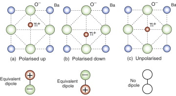
Figure 14.16 Ferro-electric materials have a permanent dipole moment that can switch: here the Ti+ ion can flip from the upper to the lower position. Above the Curie temperature the asymmetry disappears.
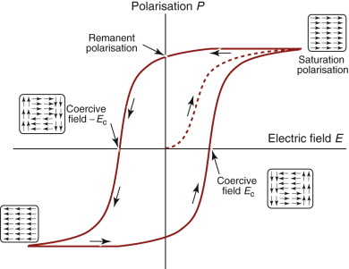
In the absence of an external field a ferro-electric divides itself up into domains—regions in which all the dipoles are aligned in one direction—separated by domain walls at which the direction of polarisation changes (Figure 14.17). The domains orient themselves so that the dipole moment of one more or less cancels those of its neighbours. If a field is applied the domain walls move so that those polarised parallel to the field grow and those polarised across or against it shrink, until the entire sample is polarised (or ‘poled’) in just one direction. Figure 14.18 shows how the polarisation P changes as the field E is increased: P increases, reaching a maximum at the saturation polarisation, Ps. If the field is now removed, a large part of the polarisation remains (the remanent polarisation), which is only removed by reversing the field to the value 2Ec, the coercive field. The figure shows a complete cycle through full reverse polarisation, ending up again with full forward poling. The little inserts show the domain structures round the cycle.
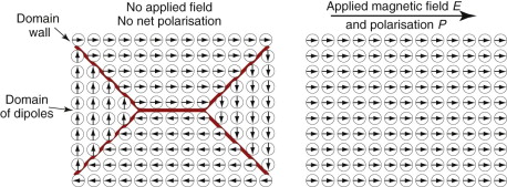
Figure 14.17 Ferro-electric domains arrange themselves so that their dipole moments cancel. In an electric field E they align, giving the crystal a net dipole moment, which can be large.
Ferro-electric materials have enormous dielectric constants. Those of normal materials with symmetric charge distributions lie in the range 2–20. Those for ferro-electrics can be as high as 20 000. It is this that allows their use to make super-capacitors that can store 1000 times more energy than conventional capacitors. Such is the energy density that super-capacitors now compete with batteries for energy storage.
14.5 Design: using the electrical properties of materials
Transmitting electrical power
The objective in power transmission is to minimise electrical loss, PL (Watts):
where i is the current (amps) and R the resistance of the transmission line, which, according to equation (14.2), is proportional to the material resistivity ρe. The best choice, for a given cross-section A, is that of a material with the lowest possible value of ρe; if the line is buried or supported along its entire length, the only other constraint is that of material cost. The chart of Figure 14.5 shows that, of the materials plotted on it, copper has the lowest resistivity, followed by aluminum. If instead the line is above ground and supported by widely spaced pylons, its strength and its density become important: high strength, to support self-weight and wind loads; low density to minimise self-weight.
Here we have a conflict: the materials with the lowest resistivity have low strength and those with high strength have high resistivities, for the reasons given in the last section. The aluminum and copper conductors used in overhead cables are those shown in Figure 14.11—precipitation hardened or work hardened to give strength with minimum loss of conductivity. Another solution is to create a hybrid cable—one in which two materials are combined, the first to give the conductivity, the second to give the strength. One such is sketched in Figure 14.19: a cable with a core of pure, high-conductivity copper or aluminum wrapped in a cage of high-strength carbon–steel wires. With a 50:50 mix the hybrid, when averaged, has roughly half the strength of the steel and twice the resistivity of the copper, a much better compromise than that offered by any single material. Many overhead cables use this approach, with a steel core surrounded by aluminum conductors; some use instead a combination of low- and high-strength aluminum alloys to reduce self-weight.
Electrical insulation
Electrical insulators keep electricity where it is supposed to be. The charts of Figures 14.6 and 14.7 show that most polymers are excellent electrical insulators, with resistivities above 1020 µΩ.cm. They are used for cable insulation, for casings of plugs, connectors and switchgear. Many ceramics, too, are good electrical insulators, notably alumina (Al2O3), silica (SiO2) and glass (Pyrex); they are used in applications in which rigidity and resistance to heat are important, such as substrates for electronic circuits and high-voltage insulators. Where electrical isolation is vital, the objective is to maximise resistivity, but as with conduction there are usually additional constraints. Here is an example.
The electric plug (Figure 14.20) is perhaps the commonest of electrical products. It has a number of components, most performing more than one function. The most obvious are the casing and the pins, though there are many more (connectors, a cable clamp, fasteners and, in some plugs, a fuse). Power plugs have two or three pins and are of robust construction. System plugs, like that of the video port of a computer, have 25 or more pins and are miniaturised and delicate, placing more importance on the mechanical as well as the electrical properties of the materials of the pins and casing. The task here is to select a material for the casing of the plug.
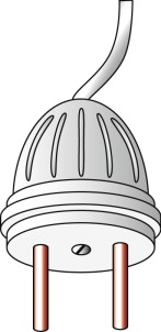
Figure 14.20 An electric plug. The casing must be an insulator, be mouldable and have sufficient strength to tolerate working loads.
The shape is complicated, the part will be made in very large numbers and pins have to be moulded in. The only practical way to make it is by using a polymer. The designers set a required strength of at least 25 MPa and, of course, the electrical resistivity should be as high as possible. The chart of Figure 14.6 suggests ABS, PMMA and PC as suitable candidates—they are strong enough and have high resistivity. But there is a problem: all three are thermoplastics; they soften if they get hot. If circuit overload or poor contact generates heat, the plug will soften, distort and even melt, presenting hazards. So the choice has to be a thermoset, which will char rather than melt. The chart suggests Phenolic—and that is what plugs are really made of. The CES software allows much more sophisticated suggestions: try the Exercises at the end of this chapter to refine the choice.
Electrical insulation with thermal conduction: keeping microchips cool
As microchips shrink in scale and clock speeds rise, overheating becomes a problem. The Pentium chip of today’s PCs already reaches 85 °C, requiring forced cooling. Multiple-chip modules (MCMs) pack as many as 130 chips on to a single substrate, and there the problem is more severe. Heating is kept under control by attaching the chips to a heat sink (Figure 14.21), taking care that they are in good thermal contact. The heat sink now becomes a critical component, limiting further development of the electronics.
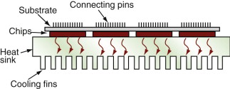
To drain heat away from the chips as fast as possible, the heat sink must have the highest possible thermal conductivity, λ. Metals like copper and aluminum have high λ, but they are good electrical conductors and this is bad because it allows electrical coupling and stray capacitance between chip and heat sink, slowing the information transfer rate (remember the time delay in a circuit is τ = RC). To prevent this, the heat sink must be an excellent electrical insulator.
Figure 14.5 is the chart with the properties we want: thermal conductivity λ and electrical resistivity ρe. The materials at the top right have high thermal conductivity and very high resistivity—they are electrical insulators. The best choice of material for the heat sink, then, is aluminum nitride (AlN), alumina (Al2O3) or silicon carbide (SiC). It is these that are used for such heat sinks.
Using dielectric loss: microwave heating
When you cook a chicken in a microwave oven, you are using dielectric loss. Looking back at equation (14.13) we see that the dielectric loss, and thus the heating, is proportional to the loss factor L = εr tan δ, one axis of the chart of Figure 14.7. Chickens do not appear on the chart, but they do have a high loss factor, as do all foods that contain water. There are other ways of cooking chicken, but this one has the advantage that it is quick because microwaves absorb uniformly through the section, giving uniform heating. Microwave heating is not just useful in the kitchen; it is also widely used for industrial heating. Wood can be dried, adhesives cured, polymers moulded and ceramics sintered using microwave heating. As equation (14.13) implies, the higher the frequency f of the electric field, the greater the heating, so it is common, in the industrial application of microwaves, to use gigahertz frequencies (0.3–3 GHz).
Using dielectric loss: stealth technology
Radar, developed during the Second World War, played a major role in protecting Britain (and others) from air attack. It works by transmitting bursts of radio-frequency waves that are reflected back by objects in their path. The radar antenna measures the time it takes for the reflection to arrive back, from which the distance and speed of the object are computed.
The metal body of an aircraft is an excellent radar reflector and its curved shape causes it to reflect in all directions—just what is needed for safe air-traffic control. But if your aim is to avoid detection, reflection is the last thing you want. Stealth technology combines three tricks to minimise it:
- A shape made up of flat planes that reflect the radar signal away from the detector unless it lies exactly normal to the surface.
- Nonmetallic structural materials—usually composites—that are semitransparent to microwaves (see Chapter 16 for how to achieve transparency).
- Surface coatings of radar-absorbing materials (called RAMs) that absorb microwaves rather than reflecting them. RAMs use dielectric loss. A surface layer of a material with a large value of loss factor εr tan δ, a ferro-electric for example, attenuates the incoming wave, diminishing the reflected signal.
Avoiding dielectric loss: materials for radomes
The function of a radome is to shield a microwave antenna from the adverse effects of wind and weather while having as little effect as possible on the signal it sends and receives (Figure 14.22). When trying to detect incoming signals that are weak to begin with, even a small attenuation of the signal as it passes through the radome decreases the sensitivity of the system. Yet the radome must withstand structural loads, loads caused by pressure difference between the inside and outside of the dome, and—in the case of supersonic flight—high temperatures. So the problem here is the opposite of stealth coatings; it is how to design materials that do not attenuate electromagnetic waves. The answer is to seek those with exceptionally low values of εr tan δ. And since the radome carries structural loads, they should also be strong.
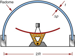
Figure 14.22 A radome. The shell must be transparent to microwaves, requiring a low dielectric loss factor with high strength.
The chart of Figure 14.7 shows that some polymers have low loss factor, but they are not very strong. Reinforcing them with glass fibres, creating GFRPs, combines low loss with good strength. When, additionally, high temperatures are involved, the ceramics that appear on the upper left of Figure 14.7—silica (SiO2), alumina (Al2O3) and silicon nitride (Si3N4)—are employed.
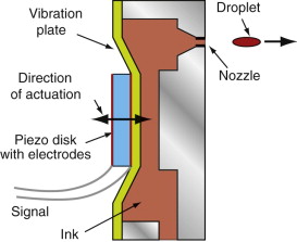
Piezo-electric actuation: ink-jet printers
Ink-jet printing is now widely used to make black and white or color prints. Many printers use thermal (‘bubble-jet’) technology, in which a tiny heating wire boils a minute volume of ink in the print-head, creating a vapour bubble. The sudden pressure this creates ejects a droplet to ink. The bubble collapses as the wire cools, sucking more ink from a reservoir into the print-head to replace that in the droplet. Very simple, but thermal technology gives little control of the droplet size or shape.
The alternative is the piezo print-head, one unit of which is sketched in Figure 14.23. An electric field applied to the disk of piezo-electric material transmits a kick to the vibration plate, creating a pressure pulse that spits a droplet of ink from the nozzle. On relaxation, more ink is drawn in to replace it. Like bubble-jet printers, piezo print-heads have 300–600 nozzles. The great advantage of piezo technology is the control of the shape and duration of the pulse delivered by the piezo disk. The droplets of ink are significantly smaller, and the control of droplet size gives greater resolution and colour gradation.
Pyro-electric thermal imaging
Night vision, the location of survivors in disaster areas, the filming of wildlife and much else make use of thermal imaging. The technology is comparatively new—the first device for two-dimensional pyro-electric imaging was developed in the late 1970s. A typical set-up is sketched in Figure 14.24. A lens, made of a material transparent to infrared (such as germanium) focuses the IR radiation from an object on the left to form an image on the pyro-electric disk on the right. The focused IR rays warm points on the disk to different degrees, depending on the temperature and emissivity of the points on the object from which they came, and the change of temperature induces local polarisation. The disk is an insulator, so the image creates a pattern of charge on the surface of the disk that can be ‘read’ with an electron beam.
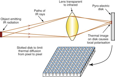
The problem with early devices was that lateral heat diffusion in the disk during the time between successive electron-beam sweeps resulted in low resolution. The problem is overcome by reticulating the surface of the disk into 20 µm islands by ion milling (a way of cutting very thin channels with a high energy ion beam), thermally isolating each island from its neighbors. Present-day imaging systems can detect a temperature change of about 0.2 °C on the target disk.
Ferro-electric actuation: injectors for diesel engines
Fuel is injected into the combustion chamber of a diesel engine by micro-pumps, one for each cylinder. To metre the fuel accurately and adapt the quantity injected to the needs of the engine, the pump must allow precise proportional control. Until recently the standard actuator for this application was a solenoid (a coil with a moving ferro-magnetic core), but to exert sufficient force to inject fuel into the high pressure in the cylinder, the solenoid had to be large and the inertia of the core limited actuation speed. The answer is to use ferro-electric actuators (Figure 14.25). Most actuators of this sort are based on the compound lead zirconium titanate (PZT). When a potential gradient dV/dx is applied across the faces of a disk of PZT, it undergoes a strain ε that is proportional to the electric potential gradient:
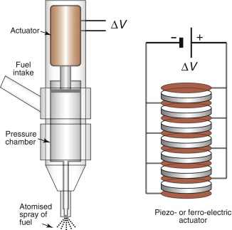
Figure 14.25 A diesel injector. The actuator of the injector must be very precise to metre the fuel accurately, and must adapt its timing and stroke to match the conditions of the engine. Piezo- or ferro-electric stacks, like that shown on the right, offer the best control.

where k is the ferro-electric coefficient of the material. In practice k is small, meaning that a high gradient is needed to get useful strain. The system voltage in cars or trucks is usually 12 or 24 V, so the only way to get a large gradient is to use very thin slices of PZT—typically 100 µm thick, giving a gradient dV/dx of 200 000 V per metre. The problem then is that the displacement (the strain ε times the thickness of the disk, x) is small. The solution is to make a stack like that shown, expanded, on the right of Figure 14.25. The thin (x = 100 µm) slices of PZT are sandwiched between conducting electrodes, alternately charged, creating the gradient. A stack of 100 (still only 10 mm high) gives adequate displacements. These actuators are half the size and allow twice the pulse rate of solenoids, giving more precise control, performance and fuel economy.
14.6 Summary and conclusions
All materials contain charged particles: electrons, protons, ions, charged molecules and the like. An electric field E exerts a force qE on a charge q, pushing it in the direction of the field if q is positive and in the opposite direction if it is negative. If the particles can move freely, as electrons can in metals, an electric current flows through the material, which we refer to as conduction. If, instead, they cannot move freely, as is the case in insulators, the particles are still displaced slightly by the field, leading to dielectric polarisation.
Materials that polarise easily have a high dielectric constant. If used as the insulating film of a capacitor, the polarisation screens the electrodes from each other, increasing the capacitance. The slight displacement of charge has other consequences. One of these is electrostriction: the charge movement causes the material to change shape slightly. If the material is made up of ions and these are arranged in a way that lacks a centre of symmetry, a further effect appears: that of piezo-electric response. The lack of symmetry means that each molecule carries a dipole moment, and within a single crystal these are aligned. An electric field causes a change of shape and a change of shape changes the molecular dipole moment, thus inducing a change in polarisation, generating a field. A change of temperature, too, changes the molecular dipole moment, so materials that are piezo-electric are also pyro-electric. A few materials have a further property: that of molecular asymmetry that can switch direction because ions can occupy one of several equivalent sites in the crystal. These materials are ferro-electric; the molecular dipoles spontaneously align to form polarised domains. In the relaxed state the domains take up orientations such that the field of one is canceled by those of its neighbours, but when ‘poled’ by placing it in an electric field, the domains align, giving a large net polarisation that is retained when the field is removed.
All these effects have practical utility, examples of which are described in the chapter.
Braithwaite N., Weaver G. Electronic Materials 1990 The Open University and Butterworth-Heinemann Oxford, UK ISBN 0-408-02840-8. (One of the excellent Open University texts that form part of their Materials program.)
Jiles D. Introduction to the Electronic Properties of Materials 2nd ed. 2001 Nelson Thornes Cheltenham, UK ISBN 0-7487-6042-3. (The author develops the electronic properties of materials, relating them to thermal and optical as well as the electrical behaviour.)
Solymar L., Walsh D. Electrical Properties of Materials 7th ed. 2004 Oxford University Press Oxford, UK ISBN 0-19-926793-6. (A mature introduction to electrical materials.)
14.8 Exercises
- Exercise E14.1 Why do metals conduct electricity? Why do insulators not conduct electricity, at least when cold?
- Exercise E14.2 What is a dielectric? What are its important dielectric properties? What is meant by polarisation? Why do some dielectrics absorb microwave radiation more than others?
- Exercise E14.3 It is much easier to measure the electrical conductivity of a material than to measure its thermal conductivity. Use the Weidemann–Franz law in Section 14.3 to find the thermal conductivities of:
- Exercise E14.4 The metal zinc has free electron concentration per unit volume, nv, of 1.3 × 1029/m3 and an electron mobility µe of 8 × 10⁻⁴ m2/V.s. The charge carried by an electron, e, is 1.6 × 10⁻¹⁹ coulomb. Based on this information, what is the electrical conductivity of zinc? Handbooks list the measured resistivity of zinc as 5.9 µΩ.cm. Is this consistent with your calculation? (Watch the units.)
Exercise E14.5 A power line is to carry 5 kA at 11 kV using pylons 460 m apart. The dip d in a wire of weight ml per unit length strung between pylons L apart at a tension T is given by d = L2ml/8T. The maximum tension allowed is 0.8 of the yield stress, σy. If the maximum allowable dip is 6 m, which of the materials in the following table could be used?
Material Electrical resistivity, ρe (Ωm) Yield stress, σy (MPa) Density, ρ (kg/m3) Aluminum 1.7 × 10⁻⁸ 102 2700 Copper 1.5 × 10⁻⁸ 300 8900 Carbon steel 55 × 10−8 510 7800 Exercise E14.6 A material is required for a transmission line that gives the lowest full-life cost over a 20-year period. The total cost is the sum of the material cost and the cost of the energy dissipated in joules. The cost of electricity CE is 6 × 10⁻³ $/MJ. Material prices are listed in the table. Derive an expression for the total cost per metre of cable in terms of the cross-sectional area A (which is a free parameter), the material and electrical costs and the material parameters. Show that the minimum cost occurs when the two contributions to the cost are equal. Hence derive a performance index for the material and decide on the best of the materials in the following table.
Material Electrical resistivity, ρe (Ωm) Density, ρ (kg/m3) Price, Cm ($/kg) Aluminum 1.7 × 10⁻⁸ 2700 1.6 Copper 1.5 × 10⁻⁸ 8900 5.2 Steel 55 × 10−8 7800 0.5 Exercise E14.7 In the discussion of conductors, a 50:50 mix of copper and steel strands was suggested for transmission cables. Using the values in the following table for resistivity and strength, calculate the effective values of both for the cable, assuming a rule of mixtures. Plot this on copies of the σy−ρe chart of Figures 14.6 and 14.11 to explore its performance.
Material Strength, σy (MPa) Resistivity, ρe (µΩ.cm) High-strength steel, cold drawn 1700 22 High-conductivity copper, cold drawn 300 1.7 Low density, we said, was important for long-span transmission lines because the self-weight becomes significant. Suppose you were asked to design a hybrid power transmission cable with the lowest possible weight, what combination of materials would you choose? Use information from the charts for inspiration.
- Exercise E14.8 Roughly 50% of all cork that is harvested in Portugal ends up as cork dust, a worthless by-product. As a materials expert, you are approached by an entrepreneur who has the idea of making useful products out of cork dust by compacting it and heating it, using microwave heating. The loss factor L of cork is 0.21. The entrepreneur reckons he needs a power density P of at least 2 kW per m3 for the process to be economic. If the maximum field E is limited to 102 V/m, what frequency f of microwaves will be needed?
14.9 Exploring design with CES (use Level 2 unless stated otherwise)
- Exercise 14.9 Use the ‘Search’ facility of CES to search for:
Exercise E14.10 The analysis of heat sinks in Chapter 3 formulated the following design constraints and objective. They are summarised in the following table. Use the selector to find the material that best meets them.
Function •Heat sink Constraints Objective •Maximise thermal conductivity Free variable •Choice of material Exercise E14.11 The sheath of the cable shown in Figure 14.19 is moulded over the bundled wires. The material of the sheath must be electrically insulating, flexible, water resistant and cheap. The following table translates the requirements. Apply the constraints using a ‘Tree’ and a ‘Limit’ stage, then plot a bar chart of material price to find the three least expensive materials that meet all the constraints.
Function •Cable sheathing Constraints Objective •Minimise material price Free variable •Choice of material Exercise E14.12 The pins of the plug of Figure 14.20 must conduct electricity well, be corrosion resistant so that contact remains good, and be hard enough to resist abrasion and wear. The following table translates the requirements. Apply these and rank the promising candidates by material price.
Function •Connecting pins for power plug Constraints Objective •Minimise material price Free variable •Choice of material Exercise E14.13 The casing of the plug of Figure 14.20 performs both a mechanical and an electrical function. It must insulate, and it must also be rigid and resilient enough to tolerate service loads. (Resilient means it must be capable of some elastic distortion requiring a high yield strain, σy/E).
Function •Plug casing Constraints Objective •Minimise material price Free variable •Choice of material
14.10 Exploring the science with CES Elements
- Exercise E14.14 Make a chart with atomic number on the x-axis (use a linear scale) and electrical conductivity κ on the y-axis. Convert the values of resistivity ρe (which are in units of µΩ.cm in the database) to those of conductivity in siemens/m (S/m); use κ = 108/ρe. This can be made using the ‘Advanced’ facility in the axis-choice dialog box. Does conductivity vary in a periodic way across the periodic table? Which three elements have the highest conductivities?
- Exercise E14.15 Explore the Wiedemann–Franz relation for the elements. To do so, make a chart of electrical conductivity, constructed as in the previous example, on the x-axis and thermal conductivity on the y-axis. Limit the selection to metals only by using a ‘Limit’ stage—State at 300 K. Fit an equation to the resulting plot. If you were now given a new alloy with an electrical conductivity of 4 × 10⁷ S/m, what would you estimate its thermal conductivity to be? (Relations such as this one provide ways of building ‘intelligent checking’ of data into material property databases.)
- Exercise E14.16 Make a chart with atomic number on the x-axis (use a linear scale) and dielectric constant on the y-axis. Do you see any general trend? If so, how would you explain it?
- Exercise E14.17 It is proposed to use the temperature dependence of electrical resistivity for sensing. Plot this quantity against relative cost to identify three cheap metals with high values of this temperature dependence.
Exercise E14.18 Equation (14.15) of the text derives the electrical conductivity as
- The CES Elements database contains data for the free electron concentration nv and the electron mobility µe. You will find the electronic charge under ‘Constants/Parameters’ in the ‘Advanced’ facility for choosing the axes of the chart. Make a chart using the ‘Advanced’ facility with κe = nveµe on the y-axis and the reciprocal of the resistivity on the x-axis. Make sure you have made all the units self-consistent. How well does this equation describe the measured conductivities of metals?
- Exercise E14.19 Explore superconductivity across the periodic table. Use CES Elements to plot superconducting transition temperature, Tc, against the atomic number (use linear scales). Which element has the highest transition temperature? What is Tc for this element?
1 George Simon Ohm (1787–1854), dropped out of his studies at the University of Erlangen, preferring billiards to mathematics, but later became absorbed in the theory of electricity and magnetism.
2 Alessandro Guiseppe Antonio Anastasio Volta (1745–1827), Italian physicist, inventor of the battery or, as it was then known, the Voltaic Pile. His face used to appear on the 10 000 lire note.
3 André Marie Ampère (1775–1836), mathematician and physicist, who, it was said, had mastered all known mathematics by the age of 14. His life was not a happy one: father guillotined during the French Revolution, miserably married and with difficult children—yet he remained extensively productive up to his death.
4 Charles Augustin Coulomb (1736–1806), military physicist, laid the foundations of both the mathematical description of electrostatic forces and the laws of friction. Despite his appointment as Intendant des Eaux et Fontaines de Paris, he made no known contributions to hydrodynamics.
5 Michael Faraday (1791–1867), brilliant experimentalist both in physics and chemistry, discoverer of electromagnetic induction and inspiring lecturer at the Royal Institution, London.
6 Wolfgang Joseph Pauli (1900–1958), quantum theorist, conceiver of the neutrino and Nobel Prize winner. He was not, however, a happy man, requiring psychotherapy, which he received from none other than the great psychoanalyst Carl Jung.
7 Enrico Fermi (1901–1954), devisor of the statistical laws known as Fermi statistics governing the behaviour of electrons in solids. He was one of the leaders of the team of physicists on the Manhattan Project for the development of the atomic bomb.
8 Theophrastus (372–287 BC), successor to Aristotle, a teacher of science and author of a 10-volume history of plants, which remained the most important contribution to botanical science for the following 1200 years.
9 Pierre Curie (1859–1906), French physicist, discoverer of the piezo-electric effect and of magnetic transformations; and husband of the yet more famous Marie Curie. He was killed in a street accident in Paris, a city with dangerous traffic even in 1906.