
Chapter 2
From Measurement to Control of
Electromagnetic Waves using a Near-field
Scanning Optical Microscope1
2.1. Introduction
The development and achievement of increasingly smaller components imposes the control of the electromagnetic field distribution on the required scales. By confining light in increasingly smaller volumes, the local amplification of the confined electromagnetic field is accompanied by a very high sensitivity of the components to the external environment.
Measurement of the electromagnetic field in structures of subwavelength size remains today a field of open application. We will present in this chapter some examples of these problems of local optical measurement, which as we will indicate finds its limits as a measurement, because on these largely subwavelength scales, the measurement can modify the properties of that which is measured.
First, we will describe the principle of local probe microscopy, limiting our description to the collection mode. We will discuss what the probe actually measures: field, intensity, etc. The measurement of the near-field in the vicinity of a surface with a random roughness will be presented. Then we will approach the measurements relating to the near-field study of integrated optic components. After the near-field characterization of photonic crystal components, a near-field measurement technique, which provides access to the amplitude and the phase of the measured signal, will be presented. Finally, the last part of this chapter will describe the interaction of the near-field probe with confined fields in very low volume cavities.
2.2. Principle of the measurement using a local probe
2.2.1. Overcoming Rayleigh's limit
In conventional microscopy, we measure an optical signal associated with the waves propagating from the measured object, which limits the resolution power. The resolving power L is the minimum distance separating two points of an object whose images are distinct. The resolving power L cannot be lower than the wavelength of the light used for illumination, and is inversely proportional to the refraction index of the environment separating the object from the lens.
![]()
n is the index of the environment, u is the opening of the beam (half wide angle at the top), λ is the wavelength of the radiation, 0.61 is the coefficient related to the Fraunhofer diffraction.
To exceed this resolution limit due to the measurement of only the propagating waves, it is necessary to detect the electromagnetic field near the object. Indeed the field resulting from the object consists of two types of waves: propagating waves and evanescent waves. These waves contain subwavelength information, but their intensity is attenuated when we move away from the object. Therefore if we need subwavelength information, it is necessary to position a probe in the immediate vicinity of the object in order to detect these evanescent waves (Ash, 1972; Pohl 1984). Detecting means that we must transform these evanescent waves into propagating waves in order to lead them to the detector. For this, different configurations exist in optics, schematized in Figure 2.1.
2.2.2. Classification of the experimental set-up
Figure 2.1. Classification of a near-field experimental set-up in light of the probe used and of the detection system
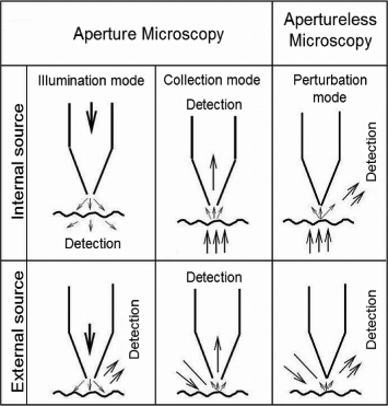
Collection mode microscopy with an opening is generally known as SNOM (Scanning near-field optical microscopy) while microscopy without an opening is called a-SNOM (a is for aperturless) (Courjon 2001; de Fornel 2001).
To these detection modes, we can add the last one, where the probe is used as a nanosource and where detection is located in the far-field. The measurement principle always involves evanescent waves, but here it is the evanescent waves that will “read” the object. The interaction of these evanescent waves with the object will generate propagating waves, which will be measured in the far-field. Once again the resolution is associated with the localization of the subwavelength source due to evanescent waves.
Other alternatives exist: fluorescent probes, probes with metal antennas, plasmonic probes. In the following we will limit ourselves to the collection mode.
2.2.3. Probe motion above a sample
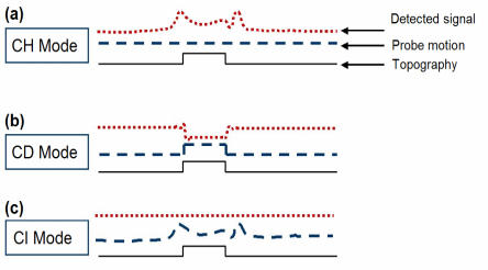
There are several ways to acquire images of the near-field: at a constant height, a constant intensity, or at a constant distance. The following figure summarizes the three modes of acquisition.
Figure 2.2. Different scanning mode for the probe. For the constant height mode, the probe scans at a fixed height above the mean plane of the surface. For the constant distance mode, the probe scans at a fixed distance from the surface. For the constant intensity, the probe scans the surface with a feedback regulation on the detected signal
2.2.4. Aperture microscope in collection mode under constant distance mode
2.2.4.1. Description of the experimental set-up
The most commonly used method is the constant distance mode. To ensure a constant distance between the probe and the surface, we use either an atomic force microscope (AFM), or a scanning tunneling microscope, for samples and metal probes. Another way of controlling the position of the probe is to use shear force control, which uses shearing forces between the surface and the probe, when it is animated by a periodic movement which is parallel to the surface of the sample. These shear forces depend directly on the distance, which separates the surface of the sample and the probe. By maintaining this constant interaction, we maintain a constant distance. Control of the distance is carried out typically on an interval varying from 0 to 20 nm. We usually work in the vicinity of 4 nm from the surface (Berguiga, 1999).
Figure 2.3 summarizes the principle of shear forces that act on the amplitude of vibration of the probe. When the probe approaches the surface the amplitude drops. By maintaining a constant amplitude, for example by detecting variations in impedance of the piezoelectric tube on which the probe can be fixed, the probe moves at a constant distance from the surface, therefore providing a topographic image.
Figure 2.3. Principle of the shear force feedback. The probe is far away from the scanning, its vibration magnitude is maximal. As the probe approaches the surface, its vibration magnitude decreases
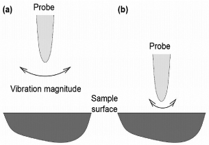
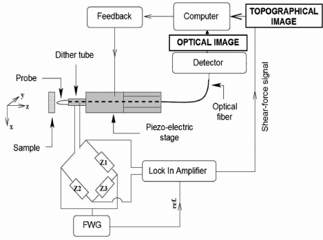
Figure 2.4 provides a diagram of a microscope in the near-field with shear force control.
Figure 2.4. Schematic view of an experimental SNOM with shear force feedback
2.2.4.2. Collection of the light
What does the near-field probe measure?
This question is not trivial. Indeed the probe located in the near-field will collect a portion of the electromagnetic field which is present in the vicinity of the object. The collection will then depend on various parameters, first of all the optogeometric characteristics of the probe (refraction index, size, modal properties, etc.) but also on the field distribution in the vicinity of the object (rate of evanescent waves, wave vectors of the propagating waves, etc.). Each experimental case is a specific case (Salomon 1991, 1999).
Consider a simple example in 2D. Figure 2.5 shows the square of the electric field in the vicinity of a nanometric object, of subwavelength size. We can note that the structure of the field is very different from the simple shape of the object and has a lateral extension much larger than the size of the object. The distribution of the square of the electric field has high amplitude oscillations along both sides of the object. What will the near-field probe measure in the vicinity of this object?
Figure 2.5. Calculation of the electric field distribution above a nanometric sized silica object. The rectangular object (100 × 100 nm2) is deposited on a silica substrate and illuminated by an incoming red (λ = 632.8 nm) plane wave under an incidence angle of 60° (i.e. total internal reflection). The plane of calculation is fixed at 10 nm above the top of the object
Consider now the probe described in Figure 2.6 which will collect and guide to the detector part of the existing field in the vicinity of the probe. We will assume that the probe moves at a constant height.
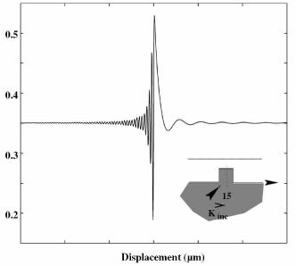
Figure 2.6. Simulation of a complete system (i.e. the probe with the sample). The simulated probe can be a chemically etched probe as well as a tapered one, with or without a metallic coating (a). In the case of a chemically etched probe (with a diameter D=25 μm, a height a1 = 20 μm and a conical angle φ =10°), for the experimental case presented in Figure 2.5. The detected signal is calculated for three different apex sizes a3 from 10 nm to 100 nm (b)
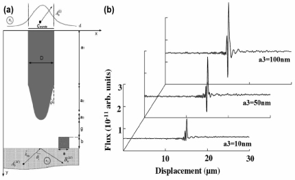
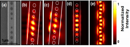
Figure 2.7 represents three simulated images for three probes of different geometry (Goumri-Said, 2005).
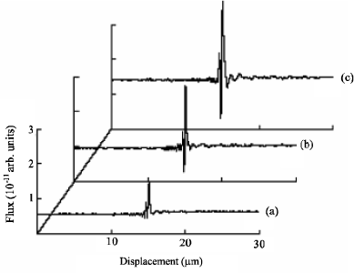
Figure 2.7. Image obtained in constant height mode of an object of 100 nm × 100 nm (g = 10 nm) with a multimode probe (D = 25 m) for φ=10° a1 = 20 m and three different apexes: (a) a3 = 10 nm; (b) a3 = 50 nm; (c) a3=100 nm
We can note that the shape of the image even if it is close to the distribution of the electric field, varies according to the shape of the probe.
We usually admit that the images of the near-field are directly related to the electric field and restore the square of the electric field. This constitutes a working basis, but it is always necessary to keep in mind that the formation of the near-field images is complex and cannot be directly linked to the square of the electric field as we will see in the last section of this chapter.
2.3. Measurement of the electromagnetic field distribution inside nanophotonic components
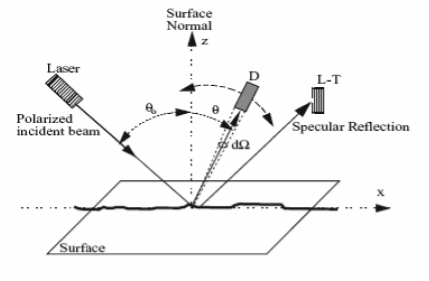
The measurement of the roughness of a surface enables its topography to be characterized, either as quality criterion for polishing for example, or to follow an evolution of its topography (aging corrosion, etc.) The roughness of a surface can be measured using an optical roughometer where for non-rough surfaces the angular analysis of the electromagnetic field diffused by surface roughnesses determines the surface roughness. This same type of measurement can be made using X-ray grazing illumination (Elson, 1979; Whitehouse, 1987; Sinha, 1988; Bennett, 1992, 1999; Deumié, 1996). The diagram in Figure 2.8 describes the principle of the optical roughometer.
Figure 2.8. Diagram of an optical roughometer. The surface is illuminated under oblique incidence (about 46°) by a monochromatic wave (λ = 632.8 nm)
We can show that the power spectral density |S(k)|2 is related to the diffused signal by the relation (Elson, 1979):
![]()
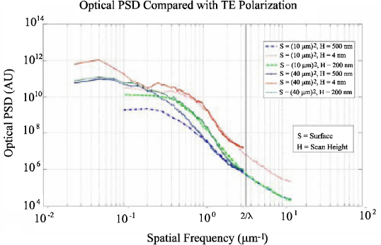
where φ0 is the incident flux, dϕ/dΩ the flux diffused in the direction θ (scattering angle) in a unit solid angle, λ is the wavelength and θ0 the incidence angle. The term |w|2is a function of θ and θ0, the permittivity ε of the sample and the polarization of the incident light. For a purely optical measurement, it is possible to determine the spectrum of power spectral density of a surface. Of course the resolution is limited to λ/2 because the measurement is carried out via the propagating waves resulting from the scattering light due to the roughnesses of the object. Near-field microscopes generally enable the topography of the objects studied to be determined. A comparison has been carried out between the spectral density curves deduced from an optical roughometer, x-ray measurements and the spectral density curves deduced from the shear force images obtained for the same samples. A good agreement was found between the different techniques for the common space frequency domain (Haidar, 2005). The measurement in the optical near-field enables the electric field distribution in the vicinity of the surface to be determined. It is therefore possible to deduce the curve of the corresponding spectral density power. In this case, we will not directly determine the spectral density of the topography but that of the electric field distribution (see Figures 2.9 and 2.10).
Figure 2.9. Spectral density curve of the topographic image of a glass blade, having undergone depolishing by chemical attack in two scanning domains of different sizes
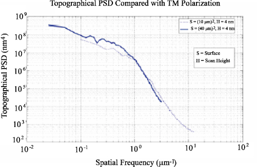
As shown in Figure 2.10, the spectral density curve associated with the optical image depends on the distance which separates the probe from the surface. Once the probe moves away from the surface, i.e. when the probe no longer detects all the evanescent fields associated with the surface (Figure 2.10), spectral frequency information higher than 2/λ is strongly reduced. Research is currently underway to refine the analysis of the relationship between topography and near-field distribution in the vicinity of the surface (Apostol, 2003, 2004).
Figure 2.10. Spectral density curves of the signal collected by the probe showing the loss of information related to high spatial frequencies when the probe moves away from the surface. The glass blade was illuminated in total reflection with λ = 0.633 μm. The probe used is a probe created by the chemical attack of a monomode fiber
2.3.1. W1 photonic crystal waveguide
In this section, we will consider two examples: a photonic crystal guide and a photonic crystal cavity.
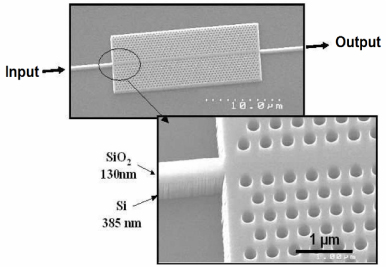
First, consider the structure created in a photonic crystal where we omit a line of holes (Figure 2.11). When the wavelength is located within the photonic band gap of the crystal, this structure behaves as a guide, noted W1. To illuminate this component, an injection guide is created upstream of the guide W1, whereas the first symmetrical extraction guide enables the light transmitted through guide W1 to be detected.
Figure 2.11. SEM view of the W1 photonic crystal waveguide
The dispersion curves of guide W1, calculated by the plane waves method in 2D for a TE polarization of the light (the electric field has components only in the plane of the photonic crystal), are presented in Figure 2.12. The dotted line represents the boundary of the light cone of the silica below which, guided modes in the silicon membrane can be coupled to the radiated modes. The two grayed areas are continuums of valence bands and conduction bands which extend modes to the entire silicon membrane.
Figure 2.12. Plane wave method simulation of the W1 photonic crystal waveguide. The band diagram (a) computed for a TE polarization exhibits a photonic band gap with two guided modes. By calculating the electromagnetic field associated to these two modes (b), it is possible to identify the parity of the modes. One is an even mode eg and the other is an odd mode og
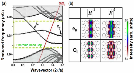
In the white space between these two areas appears the photonic band gap of the crystal without defect, where two guided modes exist. One is noted e0 and has an even field symmetry while the second, noted o0, has an odd field symmetry. This symmetry is determined depending on the axis of propagation. Distributions of the field of these two modes are also shown in Figure 2.12. These two modes are both quasi-TE and because of their orthogonality, theoretically they cannot be coupled.
The spectrum obtained by measuring the transmission of the guide (Figure 2.13) is normalized by the transmission of a guide of reference wave in order to obtain an absolute value of transmission.
Figure 2.13. Comparison between (a) the theoretical band diagram and (b) the experimental transmission spectra of a W1 photonic crystal waveguide. The experimental structure consists of a 50 period long waveguide
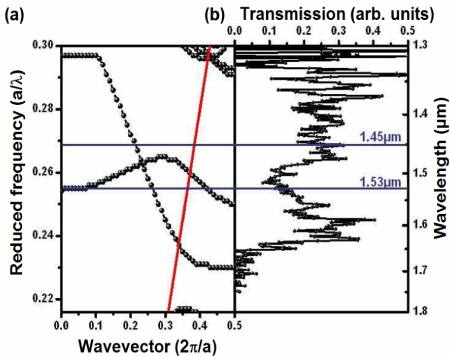
We will now record distributions of the optical near-field associated with this structure for two different wavelengths:
– at λ=1.54μm the even mode is propagated while being located above the light cone;
– at λ=1.53μm the odd and even modes are propagated. Furthermore, the transmission presents a minimum at this wavelength.
Figure 2.14. 3D view of SNOM images. The light distribution at the input and output of the waveguide at (a) 1.45 μm differs from the obtained at 1.53 μm. The topographical image (c) allows us to determine the position of the input and the output of the waveguide
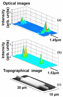
At 1.45 μm, we observe a profile of losses with a maximum collected at the input and the output centered on guide W1. Input intensity peaks are logically more important than the output peaks. From this difference, we can deduce the coupling efficiency of the fundamental mode of the conventional guide towards the even mode of W1. By neglecting the propagation losses and by integrating the measured signals, we obtain a value of 60%, identical to that deduced from transmission measurements. At 1.53 μm, a similar profile (even, with a maximum centered on W1) is observed at the guide input. On the other hand, at the output, we observe two peaks on both sides of the guide. The intensity of peaks at the output this time is more important than the input peaks. Spatial distribution of losses outside the plane depends a priori on the spatial distribution of the confined field in the guide. As the ribbon guide is a single-mode guide, the electric field of the guided mode is even with a maximum at the center. The guided mode excites the even fundamental mode of the photonic crystal guide. Losses therefore present, in theory, an even symmetry with a maximum at the center of the guide, as is observed at 1.45 μm. The situation is not the same at 1.53 μm. The profile of losses at the output present an odd symmetry, the mode at the output of the guide W1 is therefore odd. Moreover, as the output losses are higher than the input losses, the modes coupled at the input and the output are different. Also, note that the coupling efficiency between the output modes is much lower than in the input.
All of this therefore leads to the following interpretation: with 1.53 μm the even mode of guide W1 is excited at the input by the fundamental mode of the conventional guide. This is propagated in guide W1 and is coupled with the odd mode. At the output, the odd mode exists mainly in W1 and is coupled very slightly with the fundamental of the conventional guide because of their large difference in field profile. This translates as significant losses.
This result is surprising, as explained above, the even and odd modes of the guide in theory cannot be coupled: it is prohibited because of their symmetry. However, we have here experimental proof of the opposite. Let us finish the measurement analysis in the near-field before reconsidering this point.
Figure 2.15. 3D view of SNOM images. The studied wavelength is fixed (a) and (b) at 1.45 μm and (c) and (d) at 1.53 μm. The probe scans at 4 nm above the structure in (a) and (c). The probe scans at 400 nm above the structure in (b) and (d). The light propagates from left to right
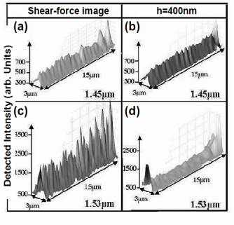
2.3.2. Photonic crystal microcavity
At 1.53 μm, the near-field signal is much higher than the far-field signal. Therefore at 4 nm from the surface we mainly measure the evanescent field. This is an additional indication of the existence of the even/odd coupling. Indeed, if at this frequency the even symmetry mode is always located above the cone of light, the odd mode is located below the cone, and therefore is not coupled to the radiated modes. Therefore, we should experimentally measure an increase in transmission and not a decrease. In fact, this reflects the poor coupling between the odd mode of W1 and the fundamental of the single mode guide collection at the output. Finally, we observe an increase in the evanescent field during the propagation. This reflects the transfer of energy from the even mode to the odd mode: the group velocity of the odd mode is lower than that of the even mode, its field is amplified. It is therefore normal that we progressively measure more signals.
We have highlighted in the optical near-field the existence of coupling between even and odd modes of a photonic crystal guide. How can this coupling be explained using prohibited theory?
In theory, two modes of opposite symmetry cannot be coupled. A probable cause of this observed coupling may lie in the existence of imperfections in the structure relating to its manufacture: roughness, imperfect verticality of the sidewall.
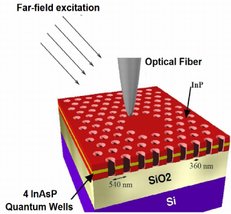
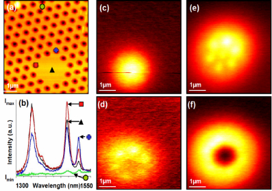
Now consider a second example, of a component with photonic crystals (Louvion, 2005; Gérard, 2004). A hexagonal cavity is created (on a suspended membrane or layer of silica) formed in a semiconductor material of InP with quantum wells at the center of the InP layer. By illuminating the structure to a wavelength of 780 nm (Figure 2.16), quantum wells will transmit by photoluminescence between 0.9 μm and 1.6 μm. This cavity is formed by a photonic crystal of hexagonal mesh, where one or more rows of holes have been omitted (H1 cavity, for the omission of a hole, H2 of 2 rows, etc.).
Figure 2.16. Schematic view of the experiment. A far-field red laser is focused on the sample surface. The photoluminescence of the quantum wells, which is locally detected by the SNOM probe, is analyzed using a spectrometer
When we measure the photoluminescence spectrum of such a cavity in the far-field, we observe a number of peaks. Each peak corresponds to the excitation of a cavity mode. To validate this assumption, measurements in the near-field have been carried out.
Except for the cavity H1, which can be single mode, cavities support several modes. We will take for example cavity H2, which has the emission spectrum given in Figure 2.16. On optical images obtained with different spectral maxima, there are different field distributions associated with different cavity modes (Lalouat, 2008b).
Figure 2.17. Spatially and spectrally resolved analysis of a H2 cavity. The geometrical parameters of the cavity can be deduced from the topographical image (a). Four different local spectra are plotted (b). The probe position, which is depicted on the topographical image, is determined in light of the C6 symmetry of the structure. The light distribution inside the cavity is mapped for each resonance wavelength visible on the near-field spectra (c) to (e)
Generally we consider that the resulting image represents the cavity mode convoluted by a Gaussian, describing the function of the probe collection (Louvion, 2005, 2006; Gérard, 2004; Kramper, 2004). For a certain number of modes this is true, but for modes presenting a field distribution with an important rate of propagating waves this is no longer suitable (Lalouat, 2008b).
The resulting image is of the intensity of the electric field associated with the cavity mode. Different groups have associated with the near-field microscope an interferential measurement, in order to be able to access the amplitude and the phase of the signal in addition to its intensity (Balistreri, 2000; Nesci, 2001; Abashin, 2006).
2.4. Measuring the amplitude and phase in optical near-field
To access the amplitude and the phase, in a heterodyne set up (see Figures 18 and 19), it is necessary to define a reference channel.
Figure 2.18. (a) Principle and (b) schematic view of a heterodyne SNOM experiment
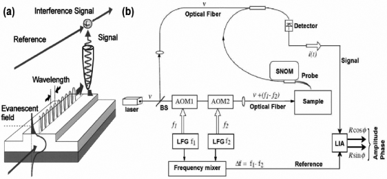
A more complete description of the circuit is presented in Figure 2.19.
Figure 2.19. SNOM schematic in heterodyne set up (Nesci, 2001)
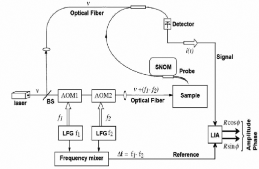
Consider a Mach-Zender interferometer and put the laser at its input. One of the interferometer arms goes directly to the detector and is used as a reference arm. Two acousto-optic modulators of similar frequencies f1 and f2 are placed on the second arm. Acousto-optic modulators are placed in such a way that enables them to produce a change of frequency on the second arm of the interferometer, whose frequency becomes v+f1−f2. The sample is then placed on the second arm of the interferometer. After collection of the signal by the optical fiber, both arms of the interferometer are connected by a fiber coupler. The output signal of the detector is sent to a synchronous detection functioning at f1−f2. Synchronous detection can work in different modes (amplitude/phase and Acosφ/Asinφ), it is possible to have a cartography of intensity, amplitude or phase of the signal.
Figure 2.20 shows the intensity conveyed by a ribbon guide, where two guided modes are propagated. The amplitude of both of the two modes should have a constant intensity according to the distance on the axis of the guide. Indeed, as the modes are orthogonal they are only added to intensity. However we note circles and nodes, this shows that the modes have been added in amplitude and phase. This observation is confirmed by the variation of the phase signal, which reveals singularities.
Figure 2.20. With the heterodyne SNOM experiment, it is possible to map experimentally the amplitude (a) and the phase (b) of the light propagating inside a ridge waveguide. Two zooms on the phase evolution map evidence phase singularities (c) and (d). The amplitude (e) and the phase (f) of the light propagating inside the waveguide is investigated numerically
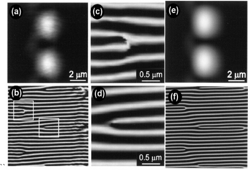
Theoretically, to find such an image, it is necessary to add modes in phase and amplitude. The different guided modes in a fiber are orthogonal to each other. Assuming the single mode probe, each mode will excite the fundamental mode of the probe with a coupling rate of α1 and α2. In the probe, the total field will be the sum in amplitude and phase of these two contributions (see equation below), therefore we will have addition in amplitude and phase.
![]()
The near-field probe, which will use the vector sum by coupling in the optical fiber, creates artifacts of measurement. The image that restores the collection mode reveals phase singularities (see Figure 2.20c and d) which in reality do not exist in the specimen vicinity.
We have seen in these different examples that detection of the near-field is not only a simple measurement of the electric field. Following the setup, and the probe type, the measured signal will not simply be equal to the square of the field.
With the reduction in the size of integrated optic components, among other things creating cavities with small volumes, we can no longer use the probe like a simple detector but rather as an active element in the operation of a cavity. From this idea the concept of the active near-field has been developed (Cluzel, 2008a,b; de Fornel, 2001).
2.5. Active optical near-field microscopy
Recent research has been carried out by some groups, which shows that a near-field probe can shift the resonance frequency of a cavity (Marki, 2006; Koenderink, 2005; Lalouat, 2007). Consider a cavity formed by two mirrors and created from a ribbon guide in silicon on a silica substrate of low modal volume V~0.6(λ/n)3~ 0.1 μm3 and whose quality factor is Q > 104. The cavity is characterized by its resonance wavelength, i.e. the wavelength for which transmittance is maximum. The probe was moved towards the surface up to 4 nm and then moved back to 100 nm (Figure 2.21). At 100 nm, we found the value of the resonance wavelength of the cavity. At 4 nm, resonance shifted towards large wavelengths. In this case, the gap was around 0.8 nm.
Figure 2.21. Tuning the cavity resonance with the near-field probe. For the two probe positions, (a) up and (b) down, two different transmission spectra are obtained
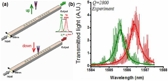
The presence of the probe will modify the cavity environment. By varying the vertical distance between the probe and the cavity, we realize that the shift in the resonance wavelength, as the quality factor value, follows exponential laws, confirming that the disturbance follows the decay law of the evanescent part of the cavity mode.
We will now focus on mapping this interaction in the optical near-field in two different ways. On the one hand, we will have the conventional mode of measurement in collection mode by the probe that we will note as ISNOM(x,y,z,λ) because the image will depend on the distance between the probe and the surface z, on the coordinates x and y and also on the injection wavelength. On the other hand, it is also possible to simultaneously record the transmission IT(x,y,z,λ) of the cavity as shown in the following Figure 2.22. These images greatly depend on the wavelength used. Here we have chosen to image the cavity to the resonance wavelength for the probe positioned at 100 nm and 4 nm from the surface (noted λup and λdown).
Figure 2.22. Experimental comparison between the interaction mode and the collection mode. The principle of the experiment identifies the detected signal (a). ISNOM corresponds to the intensity detected by the probe and IT corresponds to the transmission of the cavity. The near-field images are obtained for the resonance wavelength defined previously (b). The corresponding near-field images are presented in (c)
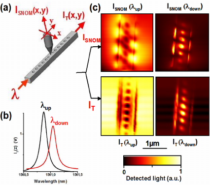
As we said earlier, the shift in wavelength and the variation of the quality factor follow the exponential decay of the evanescent field associated with the cavity mode. Thus, it is possible to imagine, initially, that a low size dielectric probe will slightly affect the cavity mode. By taking a developed approach in microwaves, we can deduce that the intensity transmitted through the cavity follows the following relation (Lalouat, 2007):
where D is a constant related to the system (probe-cavity) and w is the width at half the height of the resonance curve.
By this expression, we show that the disturbance image at λup is at first order, the inverse of the cavity mode, while at λdown it is proportional to the square of the electric field. The image in collection is more complex. It results from the disturbance of the cavity mode and the existence in the cavity of a loss mode that the probe detects, a simulation is shown in the following figure (Lalouat, 2008a).
Figure 2.23. SEM view of the studied cavity is presented in (a). The experimental results (b) and (c) can be compared to the theoretical results (d) and (e) obtained in the interaction mode (b) (d) and in the collection mode (c) and (e)
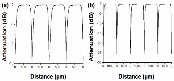
The disturbance in the near-field by an object of nanometric size enabled us to develop the concept of an active optical near-field. One of the consequences is the demonstration of the achievement of a switch, in which the interaction occurs on a nanometric scale. By moving the probe towards and away from the cavity, we can give the cavity a wavelength other than its original resonance wavelength but we can also attenuate its transmitted intensity, therefore modulating its transmitted intensity (Laouat, 2008b).
Figure 2.24. Attenuation of the transmission at the non-perturbed resonance wavelength for a cavity with a quality factor of 5,000 (a) and 10,000 (b) by controlling the distance between the probe and the cavity
2.6. Conclusion
Measurements in the optical near-field have made it possible to exceed the Rayleigh criterion which limited the optical resolution to half the wavelength of the source used to illuminate the object. This limit can be exceeded by the detection of the electromagnetic waves, which are confined in the vicinity of the object: the evanescent waves. To obtain information conveyed by these waves, probes of subwavelength sizes have been positioned in the near-field of the object. Thus it was possible to visualize the distribution of the electric field with a very high resolution subwavelength. Besides measuring the intensity of the electric field it is also possible to determine the amplitude and the phase of the near-field signal. Finally, we completed this chapter with a discussion of the development of an active optical near-field, where the probe comes to detect but also to modify the cavity properties at the same time (field distribution, resonance wavelength, etc.). This new concept opens the door for near-field components as modulators or adaptable filters in wavelength. With the continuation of miniaturization, we can easily imagine that other physical phenomena may take place such as radiation pressure, etc.
2.7. Acknowledgements
This work was carried out in collaboration with several laboratories. We would like to thank SiNaps laboratory, CEA Grenoble, LEOM, Ecole centrale Lyon, BNM Paris and Physics laboratory of Paris. Part of this work was conducted within the framework of ACI CHABIP. This work has been sponsored by the Bourgogne region by funding for scholarships and study contracts.
2.8. Bibliography
Abashin M., Tortora P., Märki I., Levy U., Nakagawa W., Vaccaro L., Herzig H.P. and Fainman Y., “Near-field characterization of propagating optical modes in photonic crystal waveguides”, Opt. Exp., vol. 14, p. 1643–1657, 2006.
Apostol A. and Dogariu A., “First- and second-order statistics of optical near fields”, Opt. Lett., vol. 29, p. 235, 2004.
Apostol A. and Dogariu A., “Spatial Correlations in the near field of random media”, Phys. Rev. Lett., vol. 91, 093901, 2003.
Ash E.A. and Nicholls G., “Super resolution aperture scanning microscope”, Nature, vol. 237, p. 510–512, 1972.
Balistreri M.L.M., Korterik J.P., Kuipers L. and van Hulst N.F. “Phase mapping of optical fields in integrated optical waveguide structures”, J. Lightwave Technology, vol. 19, p. 1169, 2001a.
Balistreri M.L.M., Gersen H., Korterik J.P., Kuipers L. and van Hulst N.F., “Tracking femtosecond laser pulses in space and time”, Nature, vol. 294, p. 1080, 2001b.
Balistreri M.L.M., Korterik J.P., Kuipers, L. and van Hulst N.F., “Local observations of phase singularities in optical fields in waveguide structures”, Phys. Rev. Lett., vol. 85, p. 294–297, 2000.
Bennett J.M. and Mattsson L., Introduction to Surface Roughness and Scattering, 2nd edn, Optical Society of America, Washington DC, US, 1999.
Bennett J.M., “Recent developments in surface roughness characterization”, Meas. Sci. Technol., vol. 3, p. 1119–1127, 1992.
Berguiga L., de Fornel F., Salomon L., Gouronnec A. and Bizeuil J., “Observation of optical fibers by near-field microscopies: effects of aging”, SPIE Proc., vol. 3848, 1999.
Born N. and Wolf E., Principles of Optics, Cambridge University Press, Cambridge, 1980.
Bozhevolnyi S.I., Volkov V.S., Sondergaard T., Boltasseva A., Borel P.I. and Kristensen M., “Near-field imaging of light propagation in photonic crystal waveguides: explicit role of Bloch harmonics”, Phys. Rev. B, vol. 66, p. 235204, 2002.
Cluzel B., Lalouat L., Velha P., Picard, E. Peyrade, D. Rodier J. C., Charvolin T. Lalanne P. de Fornel F. and Hadji E., “A near-field actuated optical nanocavity”, Opt. Exp., vol. 16, p. 279, 2008a.
Cluzel B., Lalouat L., Velha P., Picard E., Peyrade, D. Rodier J. C., Charvolin T., Lalanne P. Hadji E. and de Fornel F., “Nano-manipulation of confined electromagnetic fields with a near-field probe”, CR Physique, vol. 9, p. 24–30, 2008b.
Cluzel B., Picard E., Charvolin T., Hadji E., Lalouät L., de Fornel F., Sauvan C., Lalanne P., “Nearfield spectroscopy of low loss waveguide integrated microcavities”, Appl. Phys. Lett., vol. 88, 051112, 2006.
Cluzel B., Gérard D., Picard E.,. Charvolin T, de Fornel F. and Hadji. E. “Subwavelength imaging of field confinement in a waveguide-integrated photonic crystal cavity”, J.A.P., vol. 98, p. 086109, 2005.
Cluzel B., Gérard D., Picard E., Charvolin T., Calvo V, Hadji E., de Fornel F., “Experimental demonstration of Bloch mode parity change in photonic crystal waveguide”, App. Phys. Lett., vol. 85, no. 14, p. 2682, 2004.
Courjon D. and Bainier C., Le champ proche optique: théorie et applications, Springer, 2001.
Dändliker R., Märki I., Salt M. and Nesci A., “Measuring optical phase singularities at subwavelength resolution”, J. Opt. A, vol. 6, p. 189, 2004.
de Fornel F., Evanescent Waves, Springer, 2001.
Deumié C., Richier R., Dumas P. and Amra C., “Multiscale roughness in optical multilayers: atomic force microscopy and light scattering.” Appl. Opt., vol. 35, p. 5583–5594, 1996.
Elson J.M. and Bennett J.M., “Relation between the angular dependence of scattering and the statistical properties of optical surface”, J. Opt. Soc. Am., vol. 69, p. 31–47, 1979.
Gérard D., Etude en champ proche et en champ lointain de composants périodiquement nanostructures: cristaux photoniques et tamis à photons, PhD thesis, University of Burgundy, Dijon, 2004.
Gérard D., Berguiga L., de Fornel F., Salomon L., Seassal C., Letartre X., Rojo-Romeo P. and Viktorovitch P., “Near-field probing of active photonic crystal structures”, Opt. Lett., vol. 27, p. 173, 2002.
Gersen H., Karle T.J., Engelen R.J.P., Bogaerts W., Korterik J.P., van Hulst N.F., Krauss T.F. and Kuipers L., “Real-space observation of ultraslow light in photonic crystal waveguides”, Phys. Rev. Lett., vol. 94, p. 073903, 2005a.
Gersen H., Karle T.J., Engelen R.J.P., Bogaerts W., Korterik J.P., van Hulst N.F., Krauss T.F. and Kuipers L., “Direct observation of Bloch harmonics and negative phase velocity in photonic crystal waveguides”, Phys. Rev. Lett., vol. 94, p. 123901, 2005b.
Goumri-Said S., Salomon L., Dufour J. P., de Fornel F. and Zayats A. V., “Numerical simulations of photon scanning tunneling microscopy: role of a probe top geometry in image formation, Optics Communications, vol. 244, p. 245–258, 2005.
Greffet J.-J., “Scattering of electromagnetic waves by rough dielectric surfaces”, Phys. Rev. B, vol. 37, 6436, 1988.
Haidar Y., Berguiga L., de Fornel F., Salomon L., Gouronnec A., Zerrouki C., Pinot P., ‘Utilisation des microscopies en champ proche pour la caractérisation de surfaces de faible rugosité: application à l'étude de la fiabilité de composants’, in F. Lepoutre (ed.), Instrumentation Mesure Métrologie, Hermes – Lavoisier, p. 201–238, 2005.
Hopman W.C.L., Hollink A.J.F., de Ridder R.M., van der Werf K.O., Subramaniam V. and W. Bogaerts, “Nano-mechanical tuning and imaging of a photonic crystal micro-cavity resonance”, Opt. Exp., vol. 14, p. 8745, 2006.
Joannopoulos S., Meade R.D. and Winn J.N., Photonic Crystals: Molding the Flow of Light, Princeton University Press, 1995.
Karrai K. and Grober R.D., “Piezoelectric tip-sample distance control method for near-field scanning optical microscopes”, Appl. Phys. Lett., vol. 66, p. 1842, 1995.
Koenderink A. F., Kafesaki M., Buchler B. C. and Sandoghdar V., “Controlling the resonance of a photonic crystal microcavity by a near-field probe”, Phys. Rev. Lett., vol. 95, p. 153904, 2005.
Kramper P., Kafesaki M., Soukoulis C.M., Birner A., Müller F., Gösele U., Wehrspohn R.B., Mlynek J. and Sandoghdar V., “Near-field visualization of light confinement in a photonic crystal microresonator”, Opt. Lett., vol. 174, p. 17629, 2004.
Labilloy D., Benisty H., Weisbuch C., Krauss T.F., De La Rue R.M., Bardinal V., Houdré R., Oesterle U., Casagne D. and Jouanin C., “Quantitative measurement of transmission, reflection and diffraction of two-dimensional photonic band gap structures at near-infrared wavelengths”, Phys. Rev. lett., vol. 79, p. 4147, 1997.
Lalouat L., Cluzel B., Salomon L., Dumas C., Seassal C., Louvion N., Callard S., de Fornel F., “Real space observation of two-dimensional Bloch wave interferences in a negative index photonic crystal cavity”, accepted in Phys. Rev. B, vol. 78, p. 235304, 2008a.
Lalouat L, Cluzel B., de Fornel F., Velha P., Lalanne P., Peyrade D., Picard E., Charvolin T. and Hadji E., “Subwavelength imaging of light confinement in high-Q/small-V photonic crystal nanocavity”, Appl. Phys. Lett., vol. 92, p. 111111, 2008b.
Lalouat L., Cluzel B, Velha P., Picard E., Peyrade D., Hugonin J. P., Lalanne P., Hadji E. and de Fornel F., “Near-field interactions between a subwavelength tip and a small-volume photonic-crystal nanocavity”, Phys. Rev. B, vol. 76, p. 041102, 2007.
Loncar M., Nedeljkovic D., Pearsall T.P., Vuckovic J., Scherer A., Kuchinsky S. and Allan D.C., “Experimental and theoretical confirmation of Bloch-mode light propagation in planar photonic crystal waveguides”, Appl. Phys. Lett., vol. 80, p. 1689, 2002.
Louvion, N., Rahmani, A., Seassal, C., Callard, S., Gerard, D. and de Fornel, F., “Near-field observation of subwavelength confinement of photoluminescence by a photonic crystal microcavity”, Optics Letters, vol. 31, p. 2160–2162, 2006.
Louvion N., Gérard D., Mouette J., de Fornel F., Seassal C. Letartre,X., Rahmani A. and Callard S., “Observation and spectroscopy of optical modes in active photonic crystal microcavity”, Phys. Rev. Lett., vol. 94, p. 113907, 2005.
Marki I., Salt M., and Herzig H. P., “Tuning the resonance of a photonic crystal microcavity with an AFM probe”, Opt. Express, vol. 14, p. 2969–2978, 2006.
Monat C., Seassal C., Letartre X., Regnery P., Rojo-Romeo P., Viktorovitch P., le Vassor d'Yerville M., Cassagne D., Albert J.P., Jalaguier E., Pocas S. and Aspas B., “Two-dimensional hexagonal-shaped microcavitites formed in a two-dimensional photonic crystal on a InP membrane”, J. Appl. Phys., vol. 93, p. 23, 2003.
Mujumdar S., Koenderink A.F., Sünner T., Buchler B.C., Kamp M., Forchel A. and Sandoghdar V., “Near-field imaging and frequency tuning of a high-Q photonic crystal membrane microcavity”, Opt. Exp., vol. 15, p. 17214, 2007.
Nesci A., Measuring amplitude and phase in optical fields with sub-wavelength features, PhD thesis, University of Neuchâtel, Neuchâtel, 2001.
Pohl D.W., Demk W., Lanz M. “Optical stetoscopy: image recording with resolution lamda/20”, Appl. Phys. Lett., vol. 44, p. 651–653, 1984.
Robinson J.T., Preble S.F. and Lipson M. “Imaging highly confined modes in sub-micron scale silicon waveguides using transmission-based near-field scanning optical microscopy”, Opt. Exp., vol. 14, p. 10588, 2006.
Sakoda K., Optical Properties of Photonic Crystals, Springer-Verlag, Berlin, 2001.
Salomon L., de Fornel F and Adam P.M., “Analysis of the near-field and the far-field diffracted by a metallized grating at and beyond the plasmon resonance”, J. Opt. Soc. America A, vol. 16, p. 2695–2704, 1999.
Salomon L., de Fornel F. and Goudonnet J.P., “Sample-tip coupling efficiencies of the photon scanning tunneling microscope”, J. Opt. Soc. America A, vol. 8, p. 2009–2015, 1991.
Sauvan C., Lecamp G., Lalanne P. and J.P. Hugonin, “Modal-reflectivity enhancement by geometry tuning in photonic crystal microcavities”, Opt. Exp., vol. 13, p. 245–255, 2005.
Sinha S.K., Sirota E.B. and Garoff S., “X-ray and neutron scattering from rough surfaces”, Phys. Rev. B, vol. 38, p. 2297–2311, 1988.
Synge E., “Suggested method for extending microscopic resolution into the ultra-microscopic region”, Phyl. Mag., vol. 6, p. 356, 1928.
Uma Maheswari R., Kadono H., and Ohtsu, M. “Power spectral analysis for evaluating optical near-field images of 20 nm gold particles”, Opt. Commun., vol. 131, p. 133, 1996.
Vehla P., Rodier J.C., Lalanne P., Hugonin J.P., Peyrade D., Picard E., Charvolin T. and Hadji E., “Ultrahigh reflectivity photonic bandgap mirrors in a ridge SOI waveguide”, Appl. Phys. Lett., vol. 89, p. 171121, 2006.
Whitehouse D.J., “Surface metrology instrumentation”, J. Phys. E: Sci. Instrum., vol. 20, p. 1145–55, 1987.
Zain A.R.M., Gnan M., Chong M.H., Sorel M. and De La Rue R.M., “Tapered photonic crystal microcavities embedded in photonic wire waveguides with large resonance quality factor and high transmission”, IEEE Photonics Technol. Lett., vol. 20, p. 6, 2008.
Zerrouki C., Miserey F. and Pinot P., “Répartition angulaire de la lumière diffusée par un échantillon poli du super-alliage CoCr20WNi (alacrite XSH); application à la détermination des paramètres statistiques caractérisant la rugosité superficielle”, Eur. Phys. J. Appl. Phys., vol. 1, p. 253–259, 1998.
1 Chapter written by Loïc LALOUAT, Houssein NASRALLAH, Benoit CLUZEL, Laurent SALOMON, Colette DUMAS and FRÉDÉRIQUE dE FORNEL.