
Chapter 4
Embedded Platform Architecture
What makes an embedded platform? In this chapter we describe the constituent components that make up an embedded platform, providing details of each component and its role in the provision of an overall target solution. From the point of view of the system programmer, the focus is on the system details that are important to the embedded programmer specifically, so that the programmer can subsequently be in a position to work with a system designer in making trade-offs.
As a software developer working on embedded systems, it is very likely that you have at least a high level of familiarity with the platform, and often a very high level of detail down to the schematic level, particularly if you are developing the driver software for the target device.
Once you understand how blocks within the embedded platform are physically connected, you need to understand the view of those same components from the software/processor viewpoint. The key to understanding how the software interacts with the underlying platform devices is the system memory map and the associated register maps of the devices. Some devices are directly visible to software and mapped to physical addresses in the processor’s address space, and other devices are attached over a bus, which introduces a level of indirection when we wish to access the device registers.
In this chapter we describe the building blocks of an embedded system.
Platform Overview
Embedded platforms cover an enormous range of devices, from the residential broadband wireless router in your home to the sophisticated navigation and multimedia system in your car and the industrial control system controlling the robot that built the car. The capabilities have a broad range of interfaces and performance requirements. In the development of an embedded system you will most likely be selecting between system-on-chip devices that incorporate as many of the key peripherals your application needs. In this section we focus on the key devices required to support the operating system.
Figure 4.1 gives an overview of some of the platforms discussed in the chapter.
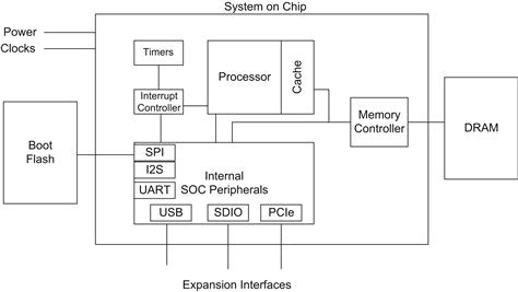
FIGURE 4.1 SOC System Overview.
Processor
Embedded systems have at least one processor. The processor is the primary execution environment for the application. The processor usually runs an operating system, and the operating system hosts the applications required to run on the platform.
In modern systems, an embedded SOC sometimes contains additional processing elements that are designed for a more specific function in support of the application. Consider a modern smartphone; the application processor is the processor that runs the software visible to the user, the user interface, or one of the many thousandths of applications such as web browser, or angry birds, mapping applications and the like. There is often another processor running the wireless stack; this is sometimes known as the baseband processor. On other platforms specific processors may process audio and camera images. The software running on these adjunct processors is often called firmware. The software execution environment for this firmware is usually specific to the target function; often they do not run an operating system. As the application power/performance efficiency and the ability to partition the application processor to run multiple execution environments (with robust quality of service) continues to improve, the trend will be to consolidate these workloads on the central processing unit.
The processor is clearly at the center of the platform. The processor in modern systems is typically 32 bit, which means that all the registers within the processor are a maximum of 32 bits wide. That includes data and address registers. Low performance embedded systems often use 16-bit microcontrollers, but the increased workload and connectivity required by such systems are driving a migration to 32-bit processors. Similarly, when high performance or large amounts of memory are required, 64-bit systems are gaining in the market.
The instruction set of the processor may be classified as either Complex Instructing Set Computing (CISC) or Reduced Instruction Set Computing (RISC). The Intel® architecture processors are all CISC-based Instruction Set Architecture (ISA), where the ARM, MIPS, and PowerPC are all considered to be RISC architecture. A CISC instruction set usually contains variable length instructions that allow for more compact encoding of the instruction. RISC, on the other hand, usually has fixed size instructions (for example, all instructions are 4 bytes long on PowerPC architecture). Some architecture, such as ARM, has introduced processors that support a subset of the original instruction set, which is recoded to improve the code density. At this point in time, from the programmer’s perspective, the distinction is less meaningful. A primary consideration is the performance achieved by the implementation.
Another aspect of the processor is whether it is scalar or superscalar. These are attributes of the microarchitecture of the processor. A superscalar-based processor supports the parallel execution of instructions by having multiple copies of key functional units within the CPU. For example, the Intel Atom™ microarchitecture contains two arithmetic logic units. The replication of key features allows the processor to sustain execution of more than one instruction per clock cycle depending on the applications and cache hit rate. The trend in embedded processors has been toward superscalar implementations, where historically many implementations were scalar.
The processor itself needs support hardware for it to perform any useful work. The key capabilities required to support the execution of a multitasking operating system on the processor are as follows:
• A memory subsystem for initial instruction storage and random access memory.
• An interrupt controller to gather, prioritize, and control generation of interrupts to the processor.
• A timer; multitasking operating systems (noncooperative) typically rely on at least one timer interrupt to trigger the operating system scheduler.
• Access to I/O devices, such as graphics controllers, network interfaces, and mouse/keypads.
The processor sits at the center of the platform and interacts with all the other devices on the platform. The locations of the devices are presented through the memory map.
System Memory Map
A key to understanding any embedded system starts with a thorough understanding of the memory map. The memory map is a list of physical addresses of all the resources on the platform, such as the DRAM memory, the interrupt controllers, and I/O devices. The system memory map is generated from the point of view of the processor. It’s important to note that there can be different points of view from different agents in the system; in particular, on some embedded devices the memory map is different when viewed from I/O devices or from devices that are attached on an I/O bus, although this is not the case on Intel platforms.
IA-32-based platforms have two distinct address spaces, memory space and input/output space. The memory space is actually the primary address space and it covers the DRAM and most I/O devices. It occupies the entire physical address space of the processor. For example, on a 32-bit system the memory space ranges from 0 to 4 GB, although not all addresses in this range map to a device or memory. Access to memory space is achieved by memory read/write instructions such as MOV. The I/O space is far smaller (only 64 kB) and can only be accessed via IN/OUT instructions. Since accesses to I/O devices through I/O space are relatively time consuming, most cases avoid use of the I/O space except for supporting legacy features (Intel platform architecture features that have been retained through the many generations of processors to ensure software compatibility). Many other embedded processor architectures such as ARM or PowerPC have only a memory address space.
When the processor generates a read or write, the address is decoded by the system memory address decoders and is eventually routed to the appropriate physical device to complete the transaction. This decision logic might match the address to that of the system DRAM controller, which then generates a transaction to the memory devices; the transaction could be routed to a hardware register in an Ethernet network controller on a PCI bus to indicate that a packet is ready for transmission.
The address map within the memory address space on Intel systems (and in fact in most systems) is split into two separate sub ranges. The first is the address range that when decoded accesses the DRAM, and the second is a range of addresses that are decoded to select I/O devices. The two address ranges are known as the Main Memory Address Range and the Memory Mapped I/O (MMIO) Range. A register in the SOC called TOLM indicates the top of local memory—you can assume that the DRAM is mapped from 1 MB to TOLM. The IA-32 memory map from zero to 1 MB is built from a mix of system memory and MMIO. This portion of the memory map was defined when 1 MB of memory was considered very large and has been retained for platform compatibility. The Memory Mapped I/O Range in which I/O devices can reside is further divided into subregions:
• Fixed Address Memory Mapped Address. There are a number of hard coded address ranges. The map is fixed and does not change. The address in this range decodes to the flash device (where BIOS/firmware is stored), timers, interrupt controllers, and some other incidental control functions. This portion of the memory map has evolved very slowly; from Intel platform to Intel platform there is a large amount of consistency.
• PCIe BUS. We provide more detail on this later, but there is a range of Memory Mapped I/O Address that will all be directed to the PCI/PCIe bus on the system. The devices that appear on the PCIe bus have configurable address decoders known as Base Address Registers (BARs). The BARs and hence the addresses occupied by the devices on the PCIe bus are provisioned as part of a bus enumeration sequence. On Intel platforms a PCIe bus logical abstraction is also used for internal devices. That means that devices within the SOC are also presented and discovered to the system software in the exact same way an external PCIe device is discovered/decoded, even though the internal devices are not connected to the processor using a real PCIe bus. For example, the graphics controller in the Intel E6xx Series SOCs appears as a PCIe device in the MMIO address space of the processor. The process of discovering and setting up the address decoders on this address range is the same for internal or external devices. There is another range of MMIO addresses, called PCI Express extended configuration register space, that can be used to generate special configuration transactions on the PCI bus so that the devices can be discovered and the BARs provisioned.
Figure 4.2 shows an overview of the system memory map for an Intel architecture platform.

FIGURE 4.2 Memory Map Representation for an Intel Platform.
The PCIe bus portion of the memory map above is not fixed. The system software (BIOS/Firmware and/or the operating system) writes to the base address register within the device at system initialization time. By contrast, in many embedded systems, the address map (within the SOC) is static. All devices are assigned an address at the time of SOC design. This does simplify the hardware design, but the system software must now be aware of the static addresses used to access each device. That usually entails building a specific target image for the target SOC. In this model it can be a little more difficult to build a single software image that supports a number of different SOC devices. Having said that, in many cases the embedded systems software is targeted and tuned to a specific device.
Interrupt Controller
The processor requires the ability to interact with its environment through a range of input and output devices. The devices usually require a prompt response from the processor in order to service a real world event. The devices need a mechanism to indicate their need for attention to the processor. Interrupts provide this mechanism and avoid the need for the processor to constantly poll the devices to see if they need attention. Given that we often have multiple sources of interrupt on any given platform, an interrupt controller is needed. The interrupt controller is a component that gathers all the hardware interrupt events from the SOC and platform and then presents the events to the processor. At its fundamental level, the interrupt controller routes events to the processor core for action. The interrupt controller facilitates the identification of the event that caused the interrupt so that the exception processing mechanism of the processor can transfer control to the appropriate handling function. Figure 4.3 shows the simplest possible form of interrupt controller. It consists of three registers that can be read from or written to from the processor. The registers are composed of bit fields with a single bit allocated for each interrupt source within each register. The first is an interrupt status register. This reflects the current pin status for the incoming interrupt line. It will be set when the interrupt request is active and clear (0) when there is no pending interrupt from the device. The second register is an interrupt mask register. Pending interrupts from the device can be prevented from getting to the processor core through the use of the interrupt mask. If the interrupt bit is set in the interrupt mask register, no interrupts from the source will reach the processor interrupt line. The interrupt status register shows the unmasked state of the interrupt line. Any of the active unmasked interrupts are capable of generating an interrupt to the processor (all signals are logically ORed together).

FIGURE 4.3 Basic Interrupt Controller Functions.
In this simplistic case, we have a single interrupt line to the processor. When the interrupt line becomes active, the processor saves a portion of the processor’s state and transfers control to the vector for external processor interrupts. This example is quite common in ARM architecture devices. The interrupt handler reads the interrupt status register and reads the active status bits in a defined priority order. A common implementation is to inspect the interrupt status bits from least significant bit to most significant bit, implying that the interrupts routed to the least significant bits are of higher priority in servicing than the other bits. The priority algorithm is under software control in this instance, and you may restructure the order in which interrupt status bits are checked.
The interrupt pending registers often take the form of a latched register. When an unmasked interrupt becomes active, the bit associated with the interrupt in the interrupt pending register becomes set (one). Then even if the interrupt signal is removed, the interrupt pending bit continues to be set. When the interrupt handler comes to service the interrupt, the handler must write a logic one to the bit it wishes to acknowledge (that is, indicate that the interrupt has been serviced). Bits with this behavior within a device register are known as Write One to Clear.
The processing of searching for the highest priority in the system by scanning bits adds to the time required to identify that highest priority interrupt to service. In embedded systems we are typically trying to reduce the overhead in identifying which interrupt we should service. To that end, a hardware block is introduced that takes the unmasked active interrupt sources and generates a number derived from a hardware-based priority scheme. The number reflects the highest-priority interrupt pending. The objective is to use this hardware generated number to quickly execute the appropriate interrupt handler for the interrupting device(s). This interrupt number can be obtained by one of two mechanisms. In the first mechanism, the interrupt software handler reads the register, the register value is used as an index into a software-based vector table containing function pointers, and the interrupt handler looks up the table and calls the function for the incoming vector. This scheme is frequently used in ARM devices where the architecture defines a single interrupt request line into the processor. The second mechanism used is one in which the CPU hardware itself generates an interrupt acknowledge cycle that automatically retrieves the interrupt number when the interrupt has been raised to the processor. This interrupt number is then translated to the interrupt vector that the processor will transfer control to. The interrupt handler is called in both cases; there is a level of software interaction in the first case that is avoided in the second implementation. The process of reading the interrupt vector number from the interrupt controller whether it was done by software or hardware may form part of an implicit interrupt acknowledgment sequence to the interrupt controller. This implicit acknowledgment indicates to the controller that the processor has consumed that particular interrupt; the interrupt controller then re-evaluates the highest priority interrupt and updates the register. In other controller implementations the device source of the interrupt must be first cleared and the highest priority interrupt will automatically update. Figure 4.4 shows the two schemes discussed.
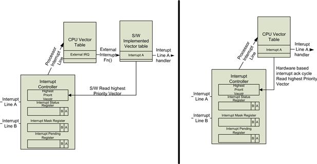
FIGURE 4.4 Interrupt Acknowledgment and Priority Schemes.
The interrupt signal designated in Interrupt A and B in Figure 4.4 may be an interrupt generated by an internal peripheral or an external general-purpose input/output (GPIO) that has interrupt generation capability. The interrupt lines typically may operate in one of the following modes:
• Level-triggered, either active high or active low. This refers to the how the logic level of the signal is interpreted. A signal that is high and is configured as active high indicates that the interrupt request is active; conversely, a low signal indicates that there is no interrupt request. The opposite is the case for an active low level triggered interrupt. Level triggered interrupts are often used when multiple devices share the interrupt line. The interrupt outputs from a number of devices can be electrically connected together and any device on the line can assert the interrupt line.
• Edge-triggered, rising edge, falling edge, or both. In this case, the transition of the interrupt line indicates that an interrupt request is signaled. When an interrupt line transitions from a logic low to a logic high and is configured as a rising edge, the transition indicates that the device has generated an interrupt. In the falling edge configurations, the opposite transition indicates an interrupt.
As you may imagine, the system (and device drivers) must handle each interrupt type differently. A level-triggered interrupt remains active and pending to the processor until the actual signal level is changed to the inactive state. The device driver handling the level-triggered interrupt may have to perform specific operations to ensure the input signal is brought to the inactive state. Otherwise, the device would constantly generate interrupts to the processor. Edge-triggered interrupts, on the other hand, effectively self-clear the indication to the interrupt controller. In many cases devices have a number of internal events that cause the device to generate an interrupt. For edge-triggered interrupts, the interrupt handler must ensure it processes all interrupt causes from the device associated with the interrupt. Level-based interrupts, on the other hand, automatically re-interrupt the processor if the driver does not clear all of the internal device interrupt sources. Level-triggered interrupts can also be shared using wired-or configuration where any device attached to the line can bring the line interrupt request line active.
Intel Architecture Specifics
The Intel architecture platform has evolved over many years and has maintained backward compatibility for a number of platform features, not just the instruction set architecture. As a result, two different interrupt controllers are available on Intel platforms. The first mechanism is the 8259 Programmable Interrupt Controller, and the second, more modern controller is known as the Advanced Programmable Interrupt Controller (APIC).
The APIC accepts interrupt messages from I/O devices (within the SOC and external PCIe devices). These messages are known as message signal interrupts (MSIs). Message signal interrupts are used by modern PCI devices (both logically on the platform and external devices). The APIC has replaced the use of 8259 PIC in most use cases, but the 8259 PIC still exists on all platforms and is often used by older operating systems. The use of the 8259 PICs is known as legacy mode at this point.
Legacy Interrupt Controller. The 8259 PIC consist of eight interrupt request lines. This was soon found to be insufficient, so the traditional configuration is to have two PIC devices, arranged in a cascaded fashion. This results in support for a total of 15 interrupt request lines. The arrangement is known as master and slave. The master PIC is wired to the processor, and the slave interrupt out signal is wired as an input to one of the master IRQ lines (IRQ2). Figure 4.5 shows cascading 8259 PICs.
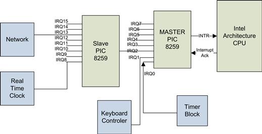
FIGURE 4.5 Cascaded 8259 Interrupt Controllers.
When an interrupt arrives at the PIC (let’s use the master for the example), the PIC updates an internal interrupt vector register and raises the interrupt to the processor. The vector register contains the value of the base vector plus the IRQ number. The base vector is a value the software has previously written as part of the interrupt controller initialization. The base line value is usually set to 0x20 to avoid the lower processor interrupts.
When the master PIC raises the interrupt request line to the processor, the processor automatically responds with a query to identify the vector through the use of an interrupt acknowledgment cycle. This is a hardware-generated sequence that prompts the interrupt controller to provide the interrupt vector to the processor. The processor then transfers control to (take) that interrupt vector, saving any required processor state as needed.
The interrupt must also be acknowledged by the software. This is carried out by writing to EOI register in both the master and slave PICs. Each interrupt controller uses two addresses in the I/O space. The I/O addresses to access the PIC(s) are
• Master PIC Command address – 0x0020
• Master PIC Interrupt Mask – 0x0021
A number of registers are associated with the interrupt processing; they are an example of a specific implementation that is similar to the examples described above in general form.
• Interrupt Request Register (IRR). The IRR is used to store all the interrupt levels that are requesting service.
• Interrupt In-Service (ISR). The ISR is used to store all the interrupt levels that are being serviced.
• Interrupt Mask Register (IMR). The IMR stores the bits that mask the interrupt lines to be masked. The IMR operates on the IRR. Masking of a higher priority input does not affect the interrupt request lines of lower priority.
There is a block that prioritizes the presentation of the interrupts. It determines the priorities of the bits set in the IRR. The highest priority is selected and strobed into the corresponding bit of the ISR during the interrupt acknowledgment cycle (INTA). The vector corresponding to this highest priority interrupt is presented to the processor. The priority encoded has a simple priority (lower number, higher priority) and a rotating priority scheme that can be configured.
The PICs can be disabled by writing 0xFF for the PIC data output address for both PIC devices. The PIC must be disabled in order to use the APIC interrupt model.
The 8259 PIC model has a number of limitations in the number of interrupts it supports and poor support for interrupt control and steering for multicore platforms. The latency of delivery of interrupt is relatively higher than other methods since it takes a number of steps before an interrupt is finally delivered to CPU.
Advanced Programmable Interrupt Controller. The Advanced Programmable Interrupt Controller or APIC was first introduced in the Intel Pentium® processor. The APIC consists of two separate key components. The first is one or more local APICs, and the second is one or more I/O APICs. The local APIC is an integral part of the each processor (for hyper-threaded processors each hardware thread has a local APIC). The local APIC performs two primary functions for the processor:
• It receives interrupts from the processor’s interrupt pins, from internal sources, and from an I/O APIC (or other external interrupt controller). It sends these to the processor core for handling.
• In multiple processor (MP) systems, it sends and receives interprocessor interrupt (IPI) messages to and from one or more logical processors on the internal or bus. IPI messages can be used to distribute interrupts among the processors in the system or to execute system-wide functions (such as booting up processors or distributing work among a group of processors).
The I/O APIC is integrated into Intel Atom–based SOC devices such as the Intel Atom Processor E6xx Series. Its primary function is to receive external interrupt events from the system and its associated I/O devices and relay them to the local APIC as interrupt messages. In MP systems, the I/O APIC also provides a mechanism for distributing external interrupts to the local APICs of selected processors or groups of processors on the system bus. The ability to steer interrupts to a target processor is often a key in embedded systems, where you are trying to carefully balance loads on the system. Figure 4.6 shows the configuration of the local and I/O APICs (although most SOC implementations do not expose the LINT0/1 pins).
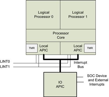
FIGURE 4.6 Local and I/O APIC Layout.
Each local APIC consists of a set of APIC registers (see Table 4.1) and associated hardware that control the delivery of interrupts to the processor core and the generation of IPI messages. The APIC registers are memory mapped and can be read and written to using the MOV instruction.
Table 4.1. Local APIC Register Map (Portion)
| Address | Register Name | Software Read/Write |
| FFE0 0000h | Reserved | |
| FFF0 0010h | Reserved | |
| FFF0 0020h | Local APID ID Register | Read/Write |
| FFF0 0030h | Local APIC Version | Read only |
| … | Other registers such as task priority, EOI | |
| FFF0 0100h | In Service Register – Bits 0:31 | Read only |
| FFF0 0110h | In Service Register – Bits 32:63 | Read only |
| FFF0 0120h | In Service Register – Bits 64:95 | Read only |
| FFF0 0130h | In Service Register – Bits 96:127 | Read only |
| FFF0 0140h | In Service Register – Bits 128:159 | Read only |
| FFF0 0150h | In Service Register – Bits 160:191 | Read only |
| FFF0 0160h | In Service Register – Bits 192:223 | Read only |
| FFF0 0170h | In Service Register – Bits 224:255 | Read only |
| … | Other registers | |
| FFF0 0320h | LVT Timer Register | Read/Write |
| FFF0 0330h | LVT Thermal Sensor Register | Read/Write |
| FFF0 0340h | LVT Performance Register | Read/Write |
| FFF0 0350h | LVT Local Interrupt 0 – LINT0 | Read/Write |
| FFF0 0360h | LVT Local Interrupt 1 – LINT1 | Read/Write |
Local APICs can receive interrupts from the following sources:
• Locally connected I/O devices. These interrupts originate as an edge or level asserted by an I/O device that is connected directly to the processor’s local interrupt pins (LINT0 and LINT1) on the local APIC. These I/O devices may also be connected to an 8259-type interrupt controller that is in turn connected to the processor through one of the local interrupt pins.
• Externally connected I/O devices. These interrupts originate as an edge or level asserted by an I/O device that is connected to the interrupt input pins of an I/O APIC. Interrupts are sent as I/O interrupt messages from the I/O APIC to one or more of the processors in the system.
• Interprocessor interrupts (IPIs). An IA-32 processor can use the IPI mechanism to interrupt another processor or group of processors on the system bus. IPIs are used for software self-interrupts, interrupt forwarding, or preemptive scheduling.
• APIC timer–generated interrupts. The local APIC timer can be programmed to send a local interrupt to its associated processor when a programmed count is reached.
• Thermal sensor interrupts. Pentium 4 and Intel Xeon™ processors provide the ability to send an interrupt to the processor when the devices thermal conditions become critical.
• APIC internal error interrupts. When an error condition is recognized within the local APIC (such as an attempt to access an unimplemented register), the APIC can be programmed to send an interrupt to its associated processor.
Of these interrupt sources, the processor’s LINT0 and LINT1 pins, the APIC timer, and some of the other events above are referred to as local interrupt sources. Upon receiving a signal from a local interrupt source, the local APIC delivers the interrupt to the processor core using an interrupt delivery protocol that has been set up through a group of APIC registers called the local vector table or LVT. A separate entry is provided in the local vector table for each local interrupt source, which allows a specific interrupt delivery protocol to be set up for each source. For example, if the LINT1 pin is going to be used as an NMI pin, the LINT1 entry in the local vector table can be set up to deliver an interrupt with vector number 2 (NMI interrupt) to the processor core. The local APIC handles interrupts from the other two interrupt sources (I/O devices and IPIs) through its IPI message handling facilities.
The following sections describe the architecture of the local APIC and how to detect it, identify it, and determine its status. Figure 4.7 gives a functional block diagram for the local APIC. Software interacts with the local APIC by reading and writing its registers. APIC registers are memory-mapped to a 4-kB region of the processor’s physical address space with an initial starting address of FEE00000H. For correct APIC operation, this address space must be mapped to an area of memory that has been designated as strong uncacheable (UC).
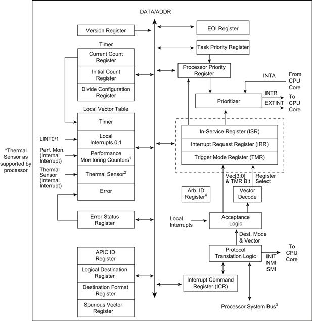
FIGURE 4.7 Local APIC Details.
The 8259 interrupt controller must be disabled to use the local APIC features; when the local APIC is disabled, the processor LINT[0:1] pins change function to become the legacy INT and NMI pins.
In multiprocessor or hyper-threaded system configurations, the APIC registers are initially mapped to the same 4-kB region of the physical address space; that is, each process can only see its own local APIC registers. Software has the option of changing initial mapping to a different 4-kB region for all the local APICs or of mapping the APIC registers for each local APIC to its own 4-kB region.
As you may have noticed, there is similarity between the 8259 and Advanced Programmable Interrupt Controllers, namely, the In-Service Interrupt Request registers. The registers, however, are much wider on the LAPIC than on the legacy interrupt controller, supporting the full range of vectors from 0 to 255. The registers are directly memory mapped (each register has a unique address in the processor memory map) and not indirectly, as is the case for the 8259-based interrupt controller. To illustrate the point, a portion of the memory map is shown in Table 4.1.
A number of interrupts are mapped directly to the local APIC; these must be assigned vectors for each source. The local APIC contains a local vector table (LVT) that associates an interrupt source with a vector number, which is provided to the processor during the interrupt acknowledge sequence. Register names that begin with LVT in Table 4.1 are used to configure the vector and mode of operation for the local interrupts, which are directly wired to the APIC.
By way of example, Figure 4.8 shows the bits definition of the LVT local interrupt 0/1 registers.
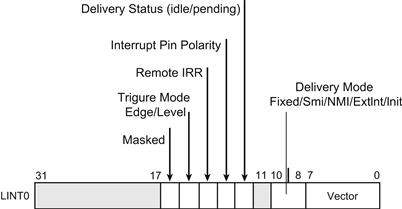
FIGURE 4.8 LVT Local Interrupt Register Definition.
As an example, setting the LVT LINT0 register value to 0x000,0020 will cause a processor interrupt with vector 32 to be generated when the processor’s local interrupt pin 0 transitions from a low to high value (active high, edge triggered).
The local APIC also accepts interrupts routed to it from PCIe devices. The PCIe devices can generate messages known as Message Signaled Interrupts. The interrupts generated by PCIe devices contain the interrupt vector to be signaled to the processor. It’s important to note that many of the internal devices on Intel systems present themselves as integrated PCIe devices. The devices themselves do not sit on a real PCIe bus, but the discovery logic and interrupt allocation mechanism do not distinguish external or internal “PCI” devices. There is more on PCIe devices later in the chapter.
Up to this point we have concentrated on the local interrupt scalability of the local APIC, but the local APIC provides a critical mechanism for other interrupt controllers in the system: a way to send interrupt requests to the processor. The I/O APIC is one such interrupt controller that is integrated into the SOC. The I/O APIC interrupt controller on Intel SOCs collects interrupt signals from with the SOC and routes the interrupt to the local APIC.
A key portion of the local APIC accepts interrupt messages from the I/O APIC. The I/O APIC on the SOC provides 24 individual interrupt sources. The I/O APIC interrupt sources are actually used within the SOC; none of the sources are brought out on pins for use as an external interrupt source. For example, the 8254 timer is connected to the I/O APIC IRQ2 pin internally. Most other pins are routed to serial interrupt request lines. The serial interrupt line is a single pin with a specific data encoding that simple devices can use to raise an interrupt. A number of devices can be daisy-chained on to the serial interrupt line and used for low pin count, low frequency interrupts. The translation between the I/O APIC interrupt source and the vector generated is contained in the I/O APIC interrupt redirection table. The table entries are similar to the LVT interrupt entry in the local APIC, but obviously reside in the I/O APIC (see Figure 4.9). There is one critical additional entry in the I/O APIC redirection table: the specification of a targeted local APIC. This allows a particular interrupt vector to be routed to a specific core or hyper-thread. The vector range for the I/O APIC is between 10h and FEh. In multiprocessor systems, the interrupts can be sent to “any” local APIC, where either core can respond to the interrupt.

FIGURE 4.9 I/O APIC Redirection Table Entry.
The I/O APIC provides just three registers that are memory-mapped to the core. Two of the three registers provide an indirect mechanism to access the registers inside the APIC. The first register is an Index register at address 0xFEC00000. This 8-bit register selects which indirect register appears in the window register to be manipulated by software. Software will program this register to select the desired APIC internal register. The second indirect register is the Window register located at address 0xFEC00010. This 32-bit register specifies the data to be read or written to the register pointed to by the Index register. This mechanism of using a few memory-mapped registers to access a larger bank of internal device registers is a common design pattern used in IA-32 systems. The third register is the EOI register. When a write is issued to this register, the IOxAPIC will check the lower 8 bits written to this register and compare it with the vector field for each entry in the I/O Redirection Table. When a match is found, the Remote Interrupt Request Register (RIRR) for that entry will be cleared. If multiple entries have the same vector, each of those entries will have RIRR cleared. Once the RIRR entry is cleared, I/OAPIC can resume accepting the same interrupt.
Figure 4.10 shows the interrupt hardware hierarchy for a uniprocessor system. The interrupts come from many different sources, and all converge at the processor with an interrupt vector number.
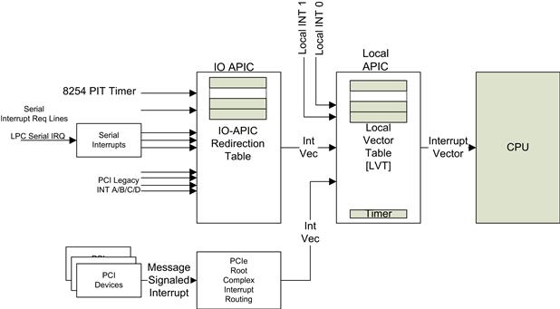
FIGURE 4.10 Interrupt Controller Hierarchy.
The software must acknowledge level-triggered interrupts by generating an EOI by writing memory-mapped EOI register in the LAPIC. The LAPIC subsequently broadcasts EOI message to all IOxAPICs in the system. The local APIC LVT registers are directly mapped, whereas the I/O APIC registers are indirectly mapped As a result, the act of writing to the local APCI LVT registers is more efficient in software.
Timers
Hardware-based timers are critical to all computer systems. A hardware-based timer generally consists of a hardware counter that counts down from a provisioned value and triggers an event such as an interrupt to the CPU when the counter reaches zero. The timer usually automatically restarts counting from the provisioned value (free-run). At least one timer is required for the operating system, particularly if it is a preemptive operating system (which most are). The operating system timer is often called the OS tick. The interrupt handler for the OS tick triggers the operating system scheduler to evaluate whether the current process should be suspended in favor of executing another ready task.
You should be aware of a number of attributes of a timer when programming it:
• Clock source. The clock source dictates the countdown interval of the timer. The clock source to a timer is usually derived by dividing one of the system clocks by a hardware divider, which can be programmed.
• Timer accuracy. The timer accuracy is largely dictated by the accuracy of the underlying clock or oscillator used to feed the timer. The accuracy of the original source is defined in parts per million (PPM). Platforms with oscillators are generally much more accurate than those that use crystals to generate the clock source. In embedded systems, the operating system tick may be used to keep track of the time of day; in this case the accuracy of the oscillator or crystal is very important. For example, a crystal source with 100 PPM will have an accuracy of 100/10e6, which is 0.01%. Given that there are 86,400 seconds in a day, a ±100 PPM crystal could be out by ±8.64 seconds per day. A good rule of thumb is that 12 PPM corresponds to approximately 1 second per day. You should note that the accuracy can vary with temperature (but within the PPM bounds specified by the manufacturer). In Intel systems, a separate real-time clock (RTC) is available. A key attribute of the RTC is that time can be maintained when power is removed from the system through the use of a battery backup. However, in deeply embedded systems a battery backup is often not used, as it would need to be replaced at some point. If the PPM of the crystal/oscillator is too high and the accuracy not acceptable, embedded platforms often rely on some external agent to provide a more accurate time of day. The Network Time Protocol is a protocol often used to acquire and maintain an accurate time of day on an embedded system. Global positioning systems also provide an accurate time stamp capability, which can be used to maintain a highly accurate time of day on the platform.
• Free run/one shot. This attribute defines the behavior of the timer itself. A free-running timer will start from a reference value and count down to zero; once the counter reaches zero the counter is reloaded with the reference value automatically and continues to count down from the reference value. The timer can be programmed to trigger an event such as an interrupt when the counter reaches zero. A one-shot timer, on the other hand, stops counting once it reaches zero. The timer must be explicitly restarted by software. Free-run mode is also referred to as periodic mode, and one shot is referred to as non-periodic mode.
• Count direction. Timers can count either down or up. The event generation value is zero for countdown timers and the reference value for count up timers.
• Counters. In this context a counter counts the clock input to the counter. The counters run freely and don’t restart automatically. The counter will start at zero and simply roll over when the counter value saturates at “all ones” in the register; that is, a 32-bit counter will roll over from 0xFFFF,FFFF to zero. Some counter registers are wider (in terms of bits) than software can read in one single read operation. For example, a 64-bit counter is often read as two individual 32-bit reads. In this case, you have to be cautious that the counter has not rolled over during the two reads. In some timer implementations a command can be issued to latch the current timer into a latch register(s). This prevents the contents from changing as the value is being read.
• Watchdog timers. These are a special class of timer. A watchdog timer (WDT) is a timer like the others, but it can usually generate an event such as a non-maskable interrupt (NMI) or reset to the hardware if the timer expires. The WDT is used to ensure that the system is restarted if the software is deemed to be nonfunctional for some reason. The software must service the WDT at adequate intervals to prevent the WDT from expiring. Embedded software uses many different strategies to make sure the overall system is operating appropriately. The simplest is to have a dedicated process that sleeps for a period, wakes up, and services the WDT. Setting the priority of this task is always tricky; under heavy loads the system may be behaving perfectly normally but does not have time to schedule the watchdog process/task. More sophisticated strategies use operating system task context switch information and software-based notifications from applications tasks to assess whether the system is behaving well. WDTs are usually set to expire in 1–2 seconds. In order to prevent the accidental servicing (such as errant software writing to a single restart register) of a watchdog timer, the timer usually requires several different register writes in a specific order to service the timer and prevent its expiration.
Figure 4.11 shows the logical configuration for a generic timer block.

FIGURE 4.11 Logical Timer Configuration.
Hardware timers are often read in a tight busy loop by software delay routines. Especially if the delay is short, for longer delays it is best to call the appropriate operating system service to allow the operating system schedule some useful work while the thread is delayed.
Intel Timers/Counters
The timer infrastructure, like most parts of the IA-32 platform, has been built up as the platform has evolved. All modern Intel architecture platforms provide the following timer capabilities:
• 253/4 Legacy PIT timer block. This timer capability has been on IA-32 platforms almost since the beginning; it has been preserved on IA-32 platforms largely for legacy compatibility but is still extensively used.
• High Precision Event Timers (HPET). This is a block of timers that are wider in resolution (32/64 bit) and directly memory-mapped to the processors address space.
• Local APIC interrupt timer that is part of the logical core.
The original timer component on IA-32 systems was known as the 8253/4. It was an external IC device on the motherboard. This external component has long since been integrated into the chipset, and in Embedded Atom SOCs it has been provided on the SOC as part of a legacy support block. It is known as the Programmable Interrupt Timer (PIT) and is often still used to provide the OS tick timer interrupt, although we recommend migration to the high precision event timers at this point. The PIT timer is sourced by a 14.31818 MHz clock. The timer provides three separate counters:
• Counter 1. Refresh request signal; this was at one point in time used to trigger the refresh cycles for DRAM memory. It is no longer used.
As we mentioned, counter 0 is the key timer used for the OS tick. The control registers listed in Table 4.2 are provided in the 8253/4.
Table 4.2. PIT Timer Registers—In/Out Space
| Port | Register Name | Software Read/Write |
| 40h | Read/Write | |
| 43h | Read/Write |
This counter 0 functions as the system timer by controlling the state of IRQ0. There are many modes of operation for the counters, but the primary mode used for operating system ticks is known as mode 3: square wave. The counter produces a square wave with a period equal to the product of the counter period (838 nanoseconds) and the initial count value. The counter loads the initial count value one counter period after software writes the count value to the counter I/O address. The counter initially asserts IRQ0 and decrements the count value by two each counter period. The counter negates IRQ0 when the count value reaches zero. It then reloads the initial count value and again decrements the initial count value by two each counter period. The counter then asserts IRQ0 when the count value reaches zero, reloads the initial count value, and repeats the cycle, alternately asserting and negating IRQ0. The interrupt is only actually caused by the transition of the IRQ0 line from low to high (rising edge).
The counter/timers are programmed in the following sequence:
1. Write a control word to select a counter; the control word also selects the order in which you must write the counter values to the counter.
2. Write an initial count for that counter by loading the least and/or most significant bytes (as required by control word bits 5, 4) of the 16-bit counter.
Only two conventions need to be observed when programming the counters. First, for each counter, the control word must be written before the initial count is written. Second, the initial count must follow the count format specified in the control word (least significant byte only, most significant byte only, or least significant byte and then most significant byte).
Writing to the timer control register with a latch command latches (takes a snapshot copy of) the counter value so it can be read consistently, while providing a consistent copy for software to read.
The high precision event timers (HPET) are a more modern platform timer capability. They are simpler to use and are of higher precision—usually 64-bit counters. The Embedded Atom SOC platform provides one counter and three timers. The HPET are memory-mapped to a 1-kB block of memory starting at the physical address of FED00000h. Table 4.3 lists the key HPET registers.
Table 4.3. HPET Registers (Subset)
| Offset Address | Register Name | Description |
| 0000h | General capabilities and identification | The 64-bit value provides the period of the clock as input to the counter, the number of timers, and the precision of the counter. |
| 0010h | General configuration | Controls the routing of some default interrupts for the timers and a general timer enable bit. |
| 0020h | General interrupt status | In level-triggered mode, this bit is set when an interrupt is active for a particular timer. |
| 00F0h | Main counter value | Counter value: reads return the current value of the counter. Writes load the new value to the counter. |
| 0100h | Timer 0 config and capabilities | The register provides an indication of the capabilities for each timer. Not all timers have the same features. The register provides control for the one-shot/free-run mode and interrupt generation capability. Some of the timers are 64 bit, while others are 32 bit. |
| 0108h | Timer 0 Comparator Value (T0CV) | When set up for periodic mode, when the main counter value matches the value in T0CV, an interrupt is generated (if enabled). Hardware then increases T0CV by the last value written to T0CV. During runtime, T0CV can be read to find out when the next periodic interrupt will be generated. |
The HPET counter typically runs freely and always increments; the value rolls over to zero after the 64-bit value reaches all ones. If a timer is set up for periodic mode (free run), when the main counter value matches the value in T0CV, an interrupt is generated (if enabled). Hardware then increases T0CV by the last value written to T0CV. During runtime, T0CV can be read to find out when the next periodic interrupt will be generated. A timer may also be configured as a one-shot timer; this mode can be thought of as creating a single shot. When a timer is set up for nonperiodic mode, it generates an interrupt when the value in the main counter matches the value in the timer’s comparator register. On Intel Atom E600 Series timers 1 and 2 are only 32 bit, and the timer will generate another interrupt when the main counter wraps.
The next category of timer is that provided in the local APIC. The local APIC timer can be programmed to send a local interrupt to its associated processor when a programmed count is reached.
The local APIC unit contains a 32-bit programmable timer that is available to software to time events or operations. This timer is set up by programming four registers: the divide configuration, the initial-count register, the current-count register, and the Local Vector Table (LVT) timer register. The time base for the timer is derived from the processor’s bus clock, divided by the value specified in the divide configuration register. The timer can be configured through the timer LVT entry for one-shot or periodic operation. In one-shot mode, the timer is started by programming its initial-count register. The initial-count value is then copied into the current-count register and countdown begins. After the timer reaches zero, an timer interrupt is generated and the timer remains at its 0 value until reprogrammed.
In periodic mode, the current-count register is automatically reloaded from the initial-count register when the count reaches zero and a timer interrupt is generated, and the countdown is repeated. If during the countdown process the initial-count register is set, counting will restart, using the new initial-count value. The initial-count register is a read-write register; the current-count register is read-only.
The LVT timer register determines the vector number that is delivered to the processor with the timer interrupt that is generated when the timer count reaches zero. The mask flag in the LVT timer register can be used to mask the timer interrupt. The clock source to the local APIC timer may not be constant. The CPUID feature can be used to identify whether the clock is constant or may be gated while the processor is in one of the many sleep states. If CPUID Function 6:ARAT[bit 2] = 1, the processor’s APIC timer runs at a constant rate regardless of P-state transitions, and it continues to run at the same rate in deep C-states. If CPUID Function 6:ARAT[bit 2] = 0 or if CPUID function 6 is not supported, the APIC timer may temporarily stop while the processor is in deep sleep states. You need to know the behavior if you are using times to benchmark/time events in the system. The Atom processor timers continue to run even in the deep power-saving sleep states.
The IA watchdog timer provides a resolution that ranges from 1 μs to 10 minutes. The watchdog timer on the Embedded Atom SOC platform uses a 35-bit down-counter. The counter is loaded with the value from the 1st Preload register. The timer is then enabled and it starts counting down. The time at which the watchdog timer first starts counting down is called the first stage. If the host fails to reload the watchdog timer before the 35-bit down-counter reaches zero, the watchdog timer generates an internal interrupt. After the interrupt is generated, the watchdog timer loads the value from the second Preload register into the watchdog timer’s 35-bit down-counter and starts counting down. The watchdog timer is now in the second stage. If the processor still fails to reload the watchdog timer before the second timeout, the watchdog triggers one of the following events:
• Assert a General-Purpose Input/Output Pin (GPIO4 on Intel Atom E600 Series). The GPIO pin is held high until the system is reset by a circuit external to the SOC.
• Warm Reset. This triggers the CPU to restart from the startup vector.
• Cold Reset. This is a reset of the SOC device and the CPU restarts from the startup vector.
The process of reloading the WDT involves the following sequence of writes, as we mentioned to reduce the likelihood of an accidently servicing the timer.
When a watchdog restart event occurs, it is very useful for the software to understand if the watchdog timer triggered the restart. To that end, the watchdog controller has a bit that indicates if the last restart was caused by a system reset. The bit itself is not cleared as part of the system reset.
Timer Summary
The hardware timers all provide a similar set of capabilities; the mechanism of setup and control all vary depending on the platform, but at heart they are all the same. The operating system will take ownership of at least one timer in the system for its uses. The application software then most often uses operating system timer services that are derived from this single source. In some cases you will write your own software for a particular timer; then you have to develop the setup code as well as, critically, the software to handle the interrupt generated by the timer expiration. In many cases you may just want to read the counter value to implement a simple delay function that does not depend on the frequency of the processor or speed of executing a particular code sequence.
Volatile Memory Technologies
A complete embedded system is composed of many different memory technologies.
Intel platforms have two distinct address types. The first is for I/O devices; this is read using either IN/OUT assembly instructions or, more likely, using normal MOV instructions to a dedicated part of the address map known as memory-mapped I/O space (MMIO). When a program reads to an MMIO space it is routed to a device. The other key address space is memory. The memory space is mapped to memory devices on the platform such as the DRAM on the platform, a flash ROM device, or, in some SOCs, local on-die SRAM memory. The hardware block that converts internal memory transactions to access the memory device is known as a memory controller. We discuss some key attributes of the DRAM memory controller in this section.
DRAM Controllers
Dynamic random access memory is a form of volatile storage. The bit value at a memory location is stored in a very small capacitor on the device. A capacitor is much smaller than a logic gate, and therefore the densities are greater than memory technologies using logic such as caches for the processor or SRAM block on an SOC. The ratio is significant. For example, a level two cache of 1 MB is reasonably large for a cache on an embedded device, whereas a device such as the Intel Atom Processor E6xx Series supports up to 2 GB of DRAM.
Although the densities are considerably higher, the price per bit is lower. However, there is a system trade-off that takes place. The DRAM read time is usually far slower than memory that is made from logic gates, such as the CPU cache or SRAM devices (both internal or external).
The read latency is a key performance attribute of memory. Although many strategies are used in processor and cache design to reduce the effect of read latency to memory, in many cases it will directly impact the performance of the system. After all, eventually the processor will have to wait for the result of the read from memory before it can continue to make progress. In order to read a DRAM bit, a logic device must check the value stored on the capacitor for the bit. This is done using a sense amplifier. The sense amplifier takes a little time to figure out whether the bit has a charge or not.
Another key performance attribute is the overall bandwidth or throughput supported by the DRAM devices. Whereas the read latencies of DRAM technology have not been reduced at nearly the same pace as the increase in density or overall throughput performance, the throughput performance has increased dramatically over time. The key improvements in throughput performance of DRAM are accomplished by pipelining as many read and write requests to the memory devices as possible. The DRAM device duplicates many of the logic resources in the device to have many concurrent lookups (sensing) occurring. Figure 4.12 shows the increased performance through multiple parallel requests to the DRAM. DDR memories have separate requests and response lines; this allows the requester interface to enqueue multiple requests while waiting for the response to review requests.
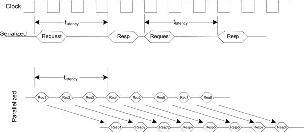
FIGURE 4.12 Increased Performance through Pipelining.
It is important that memory interfaces are standardized to allow many different manufacturers to develop compatible devices for the industry. At the time of writing, DDR2 SDRAM is the predominant DRAM type used in embedded platforms. DDR3 is becoming the DRAM technology used on mainstream compute platforms. The adoption of memory technologies in embedded platforms usually lags behind the adoption of the technology in mainstream platforms. This is often due to a price premium for the memory when it is first introduced into the market.
The DRAM interface as well as many physical attributes are standardized by JEDEC. This organization is the custodian of the DDR1, 2, and 3 SDRAM standards. These devices are known as synchronous DRAMs because the data are available synchronously with a clock line. DDR stands for double data rate and indicates that data are provided/consumed on both the rising and falling edge of the clock. As we mentioned above, the throughput of the memory technology can be increased by increasing the number of parallel requests to the memory controller. Both the depth of pipelining and the clock speed have increased from DDR1 to DDR2, and DDR3 has resulted in a significant increase in throughput throughout the generations of DRAM (see Table 4.4).
Table 4.4. DRAM Performance
| DRAM Tech | Memory Clock Speeds | Data Rates |
| DDR2 | 100–266 MHz | 400s–1066 MT/s |
| DDR3 | 100–266 MHz | 800–2133 MT/s |
The memory controller on the Intel Atom Processor E6xx Series supports DDR2-667 and DDR2-800 megatransfers per second (MT/s).
Unlike mainstream computers, embedded platforms usually solder the memory directly down on the printed circuit board (PCB). This is often due to the additional cost associated with a module and connector, or mechanical/physical concerns with respect to having the memory not soldered to the platform. Clearly, if the memory is directly soldered to the platform, there is limited scope for upgrading the memory after the product has been shipped. The ability to expand the memory in an embedded system post-shipment is not usually required. When the memory is directly soldered down, the boot loader or BIOS software is typically preconfigured to initialize the exact DRAM that has been placed on the board. However, when modules are used such as the dual in-line modules (DIMM) prevalent on mainstream computers, the BIOS or boot loader has to establish the attributes of the DIMM plugged in. This is achieved by a Serial Presence Detect (SPD) present on the DIMM modules. The SPD is an EPROM that is accessed via a serial interface SPI explained later. The EPROM contains information about the DIMM size and memory timing required. The BIOS takes this information and configures the memory controller appropriately.
The memory cells within the DRAM device are organized in the device in a matrix of rows by columns, shown in Figure 4.13. A memory transaction is split into to two phases; the first is called the Row Address Strobe (RAS). In this phase an entire row of address bits is selected from the matrix; all the bits in the row are sent to the bit sense amplifiers and then into a row buffer (also called a Page). The process of reading a row of data from the capacitors is actually destructive, and the row needs to be written back to the capacitors at some point. Before entering the second phase for the transaction, the memory controller must wait for the RAS to CAS Latency, called RAS CAS Delay (tRCD). The second phase of the transaction is called the Column Address Strobe (CAS). In this phase the word being read is selected from the previous row selected. The CAS Latency (tCL) is often a figure quoted; it is the time from the presentation of the column address strobe to getting the data back to the memory controller. It is measured in memory clocks, not nanoseconds. Once the memory transaction has been completed, a command called Precharge needs to be issued unless the next request falls in the same row. Precharge closes the memory row that was being used. RAS Precharge Time (tRP) is the time taken between the Precharge command and the next active command that can be issued. That is, the next memory transaction generally won’t start until the time has been completed (more on that later). As you can see, the overall latency performance of the memory device consists of three separate latencies. If we can continue to make use of the row that has been loaded into the sense amplifier logic, then we can get subsequent data with much lower latency. To this end the memory devices and controller support a burst memory command. This is where the subsequent data are provided with much lower latency. The typical burst size supported is 4. Given that modern processors have a cache subsystem, the burst memory command is a very useful transaction to exchange data between the cache and memory.
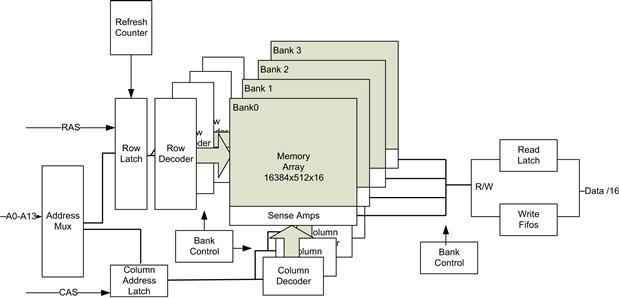
FIGURE 4.13 DDR Overview.
The normal burst mode support expects the initial address to be aligned to the size of the burst; for example, if the DRAM were a 32-bit device with a burst size of 4, the initial address for a burst would have to be 0xXXXX,XX00. The initial data returned would be for the first double word, then 0xXXXX,XX04, 0xXXXX,XX08, and lastly 0xXXXX,XX0C. If, however, the processor were waiting for the last double word in the burst (0xXXXX,XX0C), then using a burst command would decrease the performance of the processor waiting for the read result. To mitigate this, many memory controllers support a feature called Critical Word First. This CRW feature provides the data that the processor are actually waiting for first and then returns the other data elements of the burst. In the example above, the device would return the data for 0xXXXX,XX0C, 0xXXXX,XX00, 0xXXXX,XX04, and finally 0xXXXX,XX08. This would reduce the overall latency experienced by the processor but would still make use of data locality to load the cache line while the DRAM row was still active.
Another optimization to the DRAM subsystem is to have a policy on how long to keep the row buffer (page) active. As we mentioned, subsequent access to an active or open page takes less time than that required to load a new row. Given that programs often have high degrees of spatial and temporal locality, it is often best for the controller to keep a page open until a new row is accessed. This does, however, delay the time to open the new row when a new row is needed. Keeping a row active until a request is made outside that row is known as a page open policy. If the controller proactively closes the page once the transaction is complete, it is known as having a page close policy. The page sizes are relatively large; on Embedded Atom SOCs the memory controller supports devices with 1-kB, 2-kB, and 4-kB pages. Since there can be a considerable advantage to reading from an open page, the DRAM devices are partitioned into independent banks, each with its own page (row buffer) support. The SOC supports 4- and 8-bank DRAM devices. With 4–8 banks, memory controllers can thus keep multiple pages open, improving chances of burst transfers from different address streams.
In an embedded system you often have more flexibility and control over how memory is allocated and portioned in the system. A reasonable performance advantage can be seen by allocating different usage patterns to different banks. For example, a gain of approximately 5% can in some cases be achieved in a simple network router where the memory allocated to the network packets, operating system code space, and applications were all allocated from a separate banks.
The memory devices come in varying bit densities and data bus widths (x4, x8, x16, x32). The total memory required can be built up using any number of options. For example, one could use a 256-Mb device that has a 32-bit interface or two 128-Mb devices each with a 16-bit interface connected to the memory bus. The DRAM controller needs to be set up with the appropriate configuration to operate correctly. The rationale for determining the appropriate configuration usually comes down to the size of the devices on the platform and the amount of space available, as fewer higher density devices are required. The decision also has an economic dimension; higher-density memories are usually more expensive than lower-density ones.
No discussion of DRAM is complete without mentioning the refresh cycle. The DRAM cells are made up of tiny capacitors, and because a capacitor’s charge can leak away over time, this could ultimately result in in a 1 bit turning into a 0 bit. Clearly, this is not acceptable. Each row in each device must go through a refresh cycle with sufficient frequency to guarantee that the cell does not discharge. Generally, each DRAM device must be entirely refreshed within 64 ms. If a device has 8192 ROWs, then the refresh cycle must occur every 7.8 μs. The refresh cycle consists of a CAS before RAS cycle where the ROW address to memory array determines the row to be refreshed. Some DDR devices have their own refresh counter, which updates ROW address during refresh cycle; the DRAM controller just triggers the refresh cycle and does not have to keep track of refresh ROW addresses. Some platforms support a DDRx’s self-refresh capability; in this case the DRAM device performs the refresh cycle while the device is in low power mode with most of its signals tristated. This is usually used to allow the memory controller to be powered down when the system is in a sleep state, thus reducing the power required by the system in this state. The ability of a capacitor to retain charge is temperature dependent; if you develop a platform that supports an extended temperature range, the refresh rate may need to be increased to ensure data retention in memory cells. It is important to refresh with the required interval. Most of your testing will probably be done at normal room temperature, where the chance of a bit fading is relatively low. However, when your platform is deployed and experiences real-world temperatures, you really don’t want to be trying to debug the random system crashes you might experience. I’ve been there, and it’s no fun at all.
Even if the DRAM is being refreshed with the required interval, there is a small probability that a capacitor may spontaneously change its value, or an error in the reading of a bit may occur. These errors are known as soft errors and are thought to be the result of cosmic radiation, where a neutron strikes a portion of the logic or memory cell. To mitigate the effects, designers add a number of extra redundant bits to the devices. These extra bits record the parity of the other bits, or an error correcting code covering the data bits. Parity protection requires just a single bit (for 8 bits of data) and allows the controller to detect a single bit error in the memory. It cannot correct the bit error, as there is insufficient information. When a parity error is detected, the memory controller will typically generate an exception to the processor, as the value read from memory is known to be bad. Using additional protection bits, single bit errors in the data can be corrected, while double bit errors can be detected. The most popular protection used today is known as Error Correcting Code (ECC). The scheme uses 2 bits per 8 bits covered. When the memory controller detects a single bit error, it has enough redundant information to correct the error; it corrects the value on the fly and sends the corrected value to the processor. The error may still exist in the memory, so the controller may automatically write back the correct value into the memory location, or in some systems an interrupt is raised and the software is responsible for reading the address and writing back the same value (while interrupts are disabled). A double bit error cannot be corrected and will raise an exception to the processor. When any new data are written to memory, the controller calculates the new ECC value and writes it along with the data. During the platform startup, there is no guarantee that the error bits in the device are consistent with the data in the device. The boot code or in some cases the memory controller hardware has to write all memory locations once to bring corresponding ECC bits to the correct state before any DDR location is read. Since ECC has the ability to correct a single bit error, it is prudent to have a background activity that reads all memory locations over a period of time and self-correct memory location if a single bit soft error is encountered. Such a process is known as scrubbing. Since fixing single bit errors obviously prevents a double bit error from occurring, scrubbing drastically reduces memory data loss due to soft errors.
SRAM Controllers
Static random access memory is a volatile storage technology. The technology used in the creation of an SRAM cell is the same as that required for regular SOC logic; as a result, blocks of SRAM memory can be added to SOCs (as opposed to DRAM, which uses a completely different technology and is not found directly on the SOC die). The speed of SRAM is usually much faster than DRAM technologies, and SRAM often responds to a request within a couple of CPU clock cycles. When the SRAM block is placed on die, it is located at a particular position in the address map. The system software and device drivers can allocate portions of the SRAM for their use. Note that it is unusual for the operating system to manage the dynamic allocation/de-allocation from such memory; it is usually left up to the board support package to provide such features. SRAM memory is commonly allocated for a special data structure that is very frequently accessed by the processor, or perhaps a temporal streaming data element from an I/O device. In general, these SRAM blocks are not cache-coherent with the main memory system; care must be taken using these areas and they should be mapped to a noncached address space. On some platforms, portions of the cache infrastructure can be repurposed as an SRAM, the cache allocation/lookup is disabled, and the SRAM cells in the cache block are presented as a memory region. This is known as cache as RAM; some also refer to this very close low-latency RAM (with respect to the core) as tightly coupled memory.
The cells in a CPU cache are often made from high-speed SRAM cells. There is naturally a trade-off; the density of SRAM is far lower than DRAM, so on-die memories are at most in the megabyte range, whereas DRAMs is often in gigabytes.
Given that the read/write access time of SRAM memory is far faster than DRAM, we don’t have to employ sophisticated techniques to pipeline requests through the controller. SRAM controllers typically either handle one transaction at time, or perhaps pipeline just a small number of outstanding transactions with a simple split transaction bus. There is no performance advantage from accessing addressing in a line as is the case for DRAM.
You should understand the memory sub-word write behavior of the system can be lower than you might expect. As the density of the memory cells reduces, they can fall victim to errors (as in the case of DRAM), so in many cases the SRAM cells have additional redundancy to provide ECC error bits. When the software performs a sub-word write (such as a single byte), the SRAM controller must first perform a word read, merge in the new byte, and then write back the update word into the SRAM with the correct ECC bits covering the entire word. In earlier SRAM designs without ECC, the SRAM often provided a byte write capability with no additional performance cost.
Nonvolatile Storage
All embedded systems require some form of nonvolatile storage. Nonvolatile storage retains data even when the power is removed from the device. There are a range of technologies with varying storage capacities, densities, performance reliability, and size. There are two primary nonvolatile storage technologies in use today: the first and most prevalent for embedded systems is solid state memory, and the second is magnetic storage media in the form of hard drives.
Modern solid state memory is usually called flash memory. It can be erased and reprogrammed by a software driver. Flash memory read speed is relatively fast (slower than DRAM, but faster than hard drives). Write times are typically much slower than the read time. There are two distinct flash memory device types: NOR flash and NAND flash. They are named after the characteristic logic gate used in the construction of the memory cells. These two device types differ in many respects, but one key difference is that NAND flash is much higher density than NOR devices. Typically, NOR flash devices provide several megabytes of storage (at the time of writing, Spansion offered 1-MB to 64-MB devices), whereas NAND devices provide up to gigabytes of storage (devices in the 512-MB range are typical). Most commercial external solid state storage devices such as USB pen drives and SD cards use NAND devices with a controller to provide access to the device. In embedded use cases, it is usual to directly attach the flash devices to the SOC through the appropriate interface and solder the devices directly to the board.
NOR Flash
NOR flash memory devices are organized as a number of banks. Each bank contains a number of sectors. These sectors can be individually erased. You can typically continue to read from one bank while programming or erasing another. When a device powers on, it comes up in read mode. In fact, when the device is in read mode, the device can be accessed in a random access fashion: you can read any part of the device by simply performing a read cycle. In order to perform operations on the device, the software must write specific commands to specific addresses and data patterns into command registers on the device. Before you can program data into a flash part, you must first erase it. You can perform either a sector erase or full chip erase. In most use cases you will perform sector erases. When you erase a sector, it sets all bits in the sector to one. Programming of the flash can be performed on a byte/word basis.
An example code sequence to erase a flash sector and program a word is shown below. This is the most basic operation, and there are many optimizations in devices to improve write performance. This code is written for a WORD device (16-bit data bus).
//Sector Erase
// ww(address,value) : Write a Word
// See discussion on volatile in GPIO section below
unsigned short sector_address
ww(sector_address + 0x555), 0x00AA); // write unlock cycle 1
ww(sector_address + 0x2AA), 0x0055); // write unlock cycle 2
ww(sector_address + 0x555), 0x0080); // write setup command
ww(sector_address + 0x555), 0x00AA); // write additional unlock cycle 1
ww(sector_address + 0x2AA), 0x0055); // write additional unlock cycle 2
ww(sector_address) ,0x0030); // write sector erase command ∗/
.. you should now poll to ensure the command completed succesfully.
// Word Program into flash device at program_address
ww(sector_address+ 0x555), 0x00AA); // write unlock cycle 1
ww(sector_address+ 0x2AA), 0x0055); // write unlock cycle 2
ww(sector_address+ 0x555), 0x00A0); // write program setup command
ww(program_address), data); // write data to be programmed
// Poll for program completion
When programming a byte/word in a block, you can program the bytes in the block in any order. If you need to program only one byte in the block, that’s all you have to write to.
A parallel NOR interface typically consists of the following signals:
• Chip Enable: a signal to select a device, set up by an address decoder.
• Output Enable: used to signal that the device place the output on the data bus.
• Address bus: A0.A20 required number of address bits to address each byte/word in the device (directly).
• Data bus: D0–D7, (and D8–D15 for word devices). The data for a read/write are provided on the data bus.
• Write Enable: signaled when a write to the device is occurring.
• Write Protect: if active it prevents erase or writes to the flash device. As a precaution, this is hardwired on the board (perhaps with a jumper switch) or connected to a general-purpose output pin under software control.
The cycles used to access the device are consistent with many devices using a simplified address and data bus.
In order to discover the configuration of a flash device such as size, type, and performance, many devices support a Common Flash Interface. A flash memory industry standard specification [JEDEC 137-A and JESD68.01] is designed to allow a system to interrogate the flash.
Many flash devices designate a boot sector for the device. This is typically write-protected in a more robust manner than the rest of the device. Usually it requires a separate pin on the flash device to be set to a particular level to allow programming the device. The boot sectors usually contain code that is required to boot the platform (the first code fetched by the processor). The boot sector usually contains enough code to continue the boot sequence and find the location of the remaining code to boot from, and importantly it usually contains recovery code to allow you to reprogram the flash remainder of the flash device.
The initial program of flash devices that are soldered on to a platform is usually carried out through the JTAG chain. This is presented through a connector that can be attached to a JTAG programmer or ICE (see Chapter 17, “Platform Debug”). The device has access to the flash device directly and can program it by emulating the behavior of a host processor in read/writing the device.
On Intel platforms, the initial instructions fetched (BIOS or boot loader) are usually stored on a NOR flash device. The flash devices can provide either a serial or parallel interface. In most cases, a serial interface is used on Intel platforms, although many others use a parallel interface.
There are some reliability differences between NOR and NAND flash devices. NOR devices are more reliable and less susceptible to bit loss. As a result, NOR flash devices are often considered the safest memory type for storing the initial program sequence for the processor (although NAND devices do have techniques to mitigate this by duplicating copies of the boot block and adding additional ECC bits to the sectors).
With random access read/write capabilities, the NOR flash more naturally supports a mode of operation called eXecute in Place (XIP). This is where a program can run directly from the flash (without first copying the data from flash to DDR memory).
Flash devices are characterized by the number of erase cycles a device supports before it starts to fail. Current devices support up to 100,000 erase cycles per sector. If flash memory is being used for a file system or to store logs of frequently changed data, then the sectors are frequently erased and reprogrammed. Software drivers must ensure that all the activity is not focused on a small number of sectors. This strategy is known as wear leveling, and all flash file systems support the principle.
The Linux kernel uses the Memory Technology Device (MTD) interface. MTD provides a generic interface for flash devices. This layer manages the individual devices at the lowest level. There are a number of flash file systems that are also provided (with differing characteristics) built up on top of the MTD layer. The most commonly used at present is the Journaling Flash File System 2 (JFFS2).
We mentioned that erasing a block sets all bits to 1. Through programming you can convert any bit with a value of 1 to zero. You can even do this without erasing. You can never convert a 0 bit to a 1 without an erase cycle. Many flash file systems make use of this attribute to help to maintaining metadata associated with a file system.
In addition to programmable storage, many devices (NOR and NAND) offer One Time Protect/Programmable (OTP) storage. This is used to store permanent information such as a serial number IMEI/ESN information, secure boot code, or SIM-Lock. The OTP bits are programmed at the time of manufacturing and cannot be updated.
NAND Flash
In contrast to the NOR flash, NAND flash does not provide a direct random access address interface. The devices work in a page/block mode. To read the device the driver must first request a page before the data from the page can be accessed. This is not unlike other secondary storage mechanisms such as disk drives, and as such it is relatively straightforward to build a file system on top of NAND devices. Erasing and programming occur in block modes. Unlike the NOR device, the programming of a block must occur in serial fashion (incremental address programmed in order). Each block has a number of pages. The page size is typically 2 kB. The time taken to load the page into the page register is relatively slow in comparison to the subsequent reads from the page register. To improve performance, many divides contain a number of page registers.
NAND (and to a lesser extent NOR) devices may contain bad pages. These bad pages must be managed by the controller (hardware or software) that provides the interface to the device. To improve the yield of NAND devices, the devices may be released with marked bad blocks. NAND devices may start life with bad blocks and further degrade over the lifetime of the device. The bad blocks found during manufacture are typically marked in spare bits within each block. You must not erase or program pages that are marked as being bad. Also, the increased density of the NAND devices brings with it some compromises, such as a possibility of a spontaneous bit change. To ensure correct overall operation, a number of additional bits are set aside for error correct control (ECC).
A native NAND physical interface typically consists of the following signals:
• Chip Enable: a signal to select a device, set up by an address decoder.
• Write and Read: to indicate direction of access.
• Command Latch Enable: latch a command on the I/O pins.
• Address Latch Enable: latch the address.
• I/O 0–7 (0–15 for 16-bit devices): this is a multiplexed command, address, and data protocol.
• Write Protect: if active it prevents erase or writes to the flash device.
• Busy indication: used to indicate if the device can accept a command.
A NAND read operation consists of loading a page from the flash array and then reading the data from the page register. Figure 4.14 shows the representation of the page register and blocks.

FIGURE 4.14 NAND Device Representation.
The following steps are required to read from the device:
1. Issue a Read Command by placing 0x00h on I/O[0:7]. Bring command latch signal and write enable active.
2. Issue the address to read by placing each byte of the address on the I/O[0:7] bus, activating the address latch and write enable for each byte of address.
3. Issue the second cycle of the read command by placing 0x30h on the I/O[0:7] while activating the command latch and write enable signals.
4. The busy line should now go active while the flash array is being read and places the contents in the page register.
5. Data can now be clocked out of the page register; by issuing subsequent Read Enable signals, the device places data on the I/O pins.
There are device optimizations to improve the performance, but this is the general process of accessing the device. As you can see, it really is block oriented.
In order to reduce the need for both NAND and NOR devices in a system, some NAND devices provide a special boot block. The boot block is designed to be as reliable as a traditional NOR device (using additional ECC or reduced density or an actual NOR partition). This boot page is automatically placed in the read page buffer, so that a processor can start random accesses to this page when the system first boots.
NAND Interfaces
When NAND devices were first introduced into the market, no standard interface was defined. The Open NAND Flash Interface (OnFi) industry workgroup was formed in 2006 to drive the standardization for raw flash devices. The OnFi workgroup has developed a number of specifications since 2006 (http://www.onfi.org):
• ONFi 1.0 defines a standard electrical and protocol interface, including the base command set.
• Block Abstracted NAND 1.0 defines a managed NAND solution that utilizes the raw NAND interface.
• ONFi 2.0 defines a high-speed double data rate interface (synchronous) of up to 133 megatransfers/second.
• NAND connector 1.0 defines a physical connector that supports a DIMM type form factor. This allows for upgrade of density/devices, and so on.
• ONFI 2.1 increased bus speed to 200 megatransfers/second.
• ONFI 2.2 includes interruptible read/erase to allow support for high-priority reads.
Some SOCs provided a “native NAND” interface. In many cases the SOC incorporates an NAND controller, and the NAND devices are connected to the SOC via an ONFi standard interface. In other cases the interface (especially the asynchronous model) uses low level software to manage the flash transactions at a low level. In the simplest form (and probably the lowest performance) the interface can be driven by GPIO pins, as you can review in a Linux kernel driver (linux/drivers/mtd/nand/gpio.c).
NAND Controllers
As you can see, the interface to the NAND devices is complex enough that a NAND controller is required, especially if high performance is needed. The NAND controllers are usually within the SOC. A controller generally supports a DMA engine that takes a block read request and a pointer to the buffer. Then the controller issues the commands to the NAND device using the ONFi-defined mechanism, performs the NAND register read, places the results in the target memory buffer, and raises an interrupt to indicate the page has been read. An example of such a driver can be found in linux/drivers/mtd/nand/denali.c.
In many cases, the SOC does not include a NAND controller or direct support for ONFi standard NAND devices. In this case the SOC usually provides an alternative interface known as MultiMediaCard (MMC). MMC memory usually takes the form of MMC cards. The definition is now standardized under the stewardship of the JEDEC organization (http://www.jedec.org/). The definition includes a flash memory controller and the flash memory devices. Of particular interest to embedded applications is the Embedded MMC (eMMC) specification (http://www.jedec.org/standards-documents/docs/jesd84-a441). In some cases eMMC devices can be soldered down onto the motherboard. The eMMC devices consist of a controller and memory. The controller offers a higher level application interface to the SOC. The driver for MMC devices can be found in Linux/drivers/mmc. The code is split into a card-specific folder, general host files, and files specific to the MMC controller. Secure Digital (SD) memory interface is the new flash interface standard based on MMC. The standard MMC/SD host controller interface is defined by the SD Association. Most controller covers operation with SD and MMC/eMMC devices/cards. The Linux kernel supports a device driver for the SDHC host controller in linux/drivers/mmc/host/sdhc.c. The driver provides access routines to file systems such as FAT32 on the device. The I/O hub device in the Intel Atom E600 Series design provides a standard-compliant SDHC controller.
Hard Disk Drives and Solid State Drives
Hard disks have been a traditional low-cost form of mass storage in platforms for many years. The hard disk drive is a device where data are stored on circular magnetically coated platters. This form of storage has the least cost per bit of all storage types considered. There are mechanical and environmental considerations that you must consider for these forms of mass storage device, and the environmental conditions associated with embedded devices often precludes their use. Because the media is revolving on a spindle, they are sometimes known as spindle-based drives. As the cost of NAND devices has come down, a new type of storage known as the solid state drive (SSD) has become cost-effective in many embedded cases. The SSD is a drive that is made up of NAND devices and a sophisticated NAND controller. The NAND controller presents a traditional hard disk drive interface to the host. The controller takes care of all the low-level flash management including wear leveling.
The latest drive interface is Serial Advanced Technology Attachment (SATA). It is defined by the Serial ATA International Organization (www.serialata.org). It is an interface used to connect host controller adaptors to mass storage devices. It is the natural evolution of the previous Parallel ATA standard. In most platforms the host controller follows a standard register level interface known as AHCI. The AHCI standard is defined by Intel (http://www.intel.com/technology/serialata/ahci.htm).
Most controllers can be configured in legacy Parallel ATA mode or the more advanced native interface. The native high-performance mode should be used for SATA drives. This native interface is a hardware mechanism that allows software to communicate with Serial ATA devices. AHCI is a PCI class device that acts as a data movement engine between system memory and SATA devices. The host bus adaptor (controller) supports programmed I/O mode, DMA modes (which are akin to the original legacy modes on PATA devices), and a mode known as native command queuing for SATA devices. The vast majority of operating systems provide some level of support for SATA drives, especially since the controller supports the most basic of operating modes (PIO). The source for the SATA drivers can be found in Linux/drivers/ata/∗ahci∗.c.
Table 4.5 summarizes some of the relative attributes for each mass storage device.
Table 4.5. Summary of NAND and NOR Flash and SSD
| NAND Flash | NOR Flash | SSD |
| Lowest cost per bit | Higher cost per bit | Cost per bit similar to NAND |
| Slow random access | Random access | Faster than magnetic drives |
| Fast writes | Slower writes | Drive performance is based on NAND devices and controller algorithms |
| Fast erases | Slower erases | Drive performance is based on NAND devices and controller algorithms |
| Page writes only | Byte writes | Block-based device |
| Sustained sequential read performance similar to NOR | Sustained sequential or random read performance is similar | Drive performance is based on NAND devices and controller algorithms |
| Aligns with file system block semantics | Supports execute in place, similar to ROM | Supports standard file systems through traditional mass storage interfaces |
| Controller must perform some sanity checks before it can be used | Available instantly after power on | The controller must perform some NAND integrity checks before it is used |
Device Interface—High Performance
In many cases an SOC needs additional capabilities such as an external application-specific I/O device. The device interface consists of a device interface controller and a defined external interconnect to attach to an external device.
A peripheral bus interface requires a number of capabilities:
• Transaction mapping from the processor to the device address space—The device controller captures transactions directed to the memory address of the external bus and associated device, and translates the transaction (read or write) into the appropriate transaction on the expansion bus. The translation may involve adaption due to bus width changes (such as 32-bit to 16-bit), or byte order (such as endian conversions).
• Inbound transactions—For high-performances interfaces, it is important that the expansion interface allow the external devices to read and write resources in the SOC. This is often called bus mastering. This is primarily used to access memory so the device can read and write data. Without the ability to read or write system memory, the processor or a DMA controller on the device would need to move data to and from the device. When transactions are generated by the device the transaction contains an address, the address space may be different from that used by the processor; you should be aware of the system address map as viewed by the device. The address on the device interconnect is usually known as the bus address. Your software must translate the host system address to bus address if you want the DMA engine on the device to read the system address. The device interface block in the SOC will translate the inbound bus address to the system address.
• Interrupts—Interactions with a high-performance device require the ability to route interrupts from the device to the processor. This can be used to simply indicate events on the I/O device, but most frequently it is used to send service events from the DMA engine on the device. The interface ideally includes assignment and routing of interrupts as an integral part of the capability. In simple bus interfaces the interrupts are usually routed as signals on the side, in this case general-purpose I/O signals that are configured to generate interrupts.
• Physical standard—Some interface definitions also include a physical connector standard, such as card size. A physical standard allows the system to be expanded with many different capabilities. The Peripheral Component Interconnect (PCI) is an excellent example of this. There are other expansion connector standards that cover much more than a device interconnect such a ComExpress (http://www.picmg.org) (although this standard includes a PCI bus among others as part of the interconnect). In some cases, the interface supports removable/reinsertion of devices while the system is active. This is usually known as hot plug and can be key to maintaining high availability on platforms.
There are many different bus definitions, from well-standardized Peripheral Component Interconnect (PCI) to de facto standard parallel address and data bus interfaces.
Peripheral Component Interconnect (PCI)
The predominant high-performance external interface standard is PCI. PCI has been on Intel platforms for many years and has evolved from a 32-bit parallel bus to a high-speed lower-pin-count serial bus (with many lanes to scale performance). Although the PCI standard has significantly increased I/O performance with every PCI generation, the logical view of the PCI system has been kept very consistent throughout the evolution of the standard. The approach to discover and access the device has remained the same, allowing full software compatibility over PCI generations.
PCI Express (PCIe) is the third generation of the PCI standard. It is a higher-performance I/O bus used to connect peripheral devices to compute systems. PCIe is the primary peripherals interconnect used on Intel architecture systems, but it has become popular on many platforms. The PCIe standard is developed by the PCI-SIG (http://www.pcisig.com).
The PCIe standard provides the capability to identify devices attached to a PCIe bus at runtime. Once these devices are discovered, the system software can allocate resources to these devices dynamically. This process is called bus enumeration. The enumeration process allocates a range of addresses in the system address map to access the device, as well as one or more interrupt vectors. To facilitate the enumeration process, there is a special PCIe bus space known as configuration space. The PCIe configuration space size is a total of 256 MB. The bus supports device discovery and initial configuration by responding to special configuration space transactions on the bus. The configuration space is partitioned into PCIe busses (up to 256), devices per bus (up to 32), and functions within a device (up to 8 per device). This three tuple address is known as the Bus Device Function (BDF) address. The BDF address for a device depends on where it is connected to on the PCIe fabric. The function is dedicated by the design of the device. For example, if a Ethernet card has two separate Ethernet interfaces, it will mostly likely present two separate functions. The process of enumeration is a runtime search through the PCI configuration space looking for devices. Figure 4.15 shows the physical topology of a PCIe system.
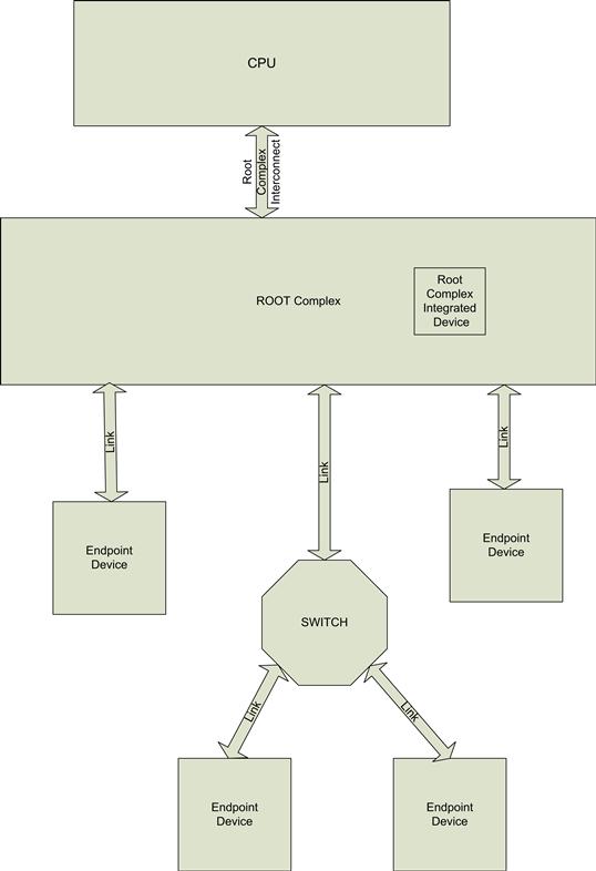
FIGURE 4.15 PCIe Physical Hierarchy.
The head of the PCIe hierarchy is known as the root complex. The root complex takes processor read/write transactions and routes them to the appropriate transaction type in the PCIe fabric. The root fabric takes upstream transactions from PCIe devices and routes them to the host memory. It also routes interrupts from the devices to the appropriate processor. Devices can also be integrated into the root complex; in this case the devices are presented in exactly the same way as devices that are attached via external physical PCIe links. This provides a consistent approach to discovering internal and external devices.
Each device has a configuration space header. Each device configuration space can be up to 256 bytes. A device can optionally have an extended capabilities register at offsets in range 256 to 4095. A total of 65,536 devices are theoretically supported on PCI. Processors cannot natively generate a PCI configuration cycle; the PCI configuration space transactions can be generated by either of the following mechanisms (on Intel architecture systems):
• Indirect mode: Use a sequence of I/O transaction to write to address port at I/O address 0xCF8 followed by read/write to Data Port register at I/O address 0xCFC. The address register is written with the PCI configuration address to read, and then content is read/written to by accessing the data port register. This mechanism allows accessing of first 256 configuration registers; extended capability registers in range [256–4095] can be assessed only through the MMIO mechanism described next.
• MMIO: Up to 256-MB (max 4K per device ∗ 65,536 devices) configuration space is mapped into the processor’s memory-mapped address space. Reads or writes to this address space generate the configuration transactions on the PCI bus.
The enhanced MMIO mode of configuration can directly access all registers of any device on the PCI bus. The MMIO address bits are built up from the following bit fields:
• A[32:28] = MMIO configuration space: base of which is set by the MMBAR register
• A[19:15] = Device number on bus
Each device must have a base configuration header. Figure 4.16 shows a base configuration header. It allows the system software to identify the device type and to assign memory and interrupts to the device.
FIGURE 4.16 PCI Configuration Header.
The vendor ID identifies the manufacturer of the function. The IDs are assigned by the PCI-SIG. The vendor ID assigned to Intel devices is, somewhat humorously, 8086h. The device ID is assigned by the manufacturer and is used to indicate the device type. This device ID is usually used by operating systems to find the appropriate device driver to load and associate with the device. The device revision can be used to adapt the driver for specific versions of the device. The Class code can for some generic devices be used to provide a generic device driver support for a device. In this case the device ID is ignored and the operating system assigns the device driver based on class code. An example where a class code for a generic device is used is a simple VGA adaptor.
PCI devices are composed of two different register spaces, the configuration space and device registers. The configuration space is primarily used as part of the enumeration and allocating the driver to the device. The configuration space contains a number of base address registers. These base address registers are programmable decoders that are used to decode access to the actual device registers. There are six 32-bit or three 64-bit base address registers. The base address register contains some read-only low-order bits set to zero. When you write all ones to the base address register and read back the value, the enumeration software establishes the size of memory the enumeration software must allocate. For example, if the software writes 0xFFFFFFFF to a base address register but reads back 0xFFFF000, then the device is requesting a space of 4 kB. The enumeration software allocates all the memory for the devices “requested” by the enumeration process and writes to all the device base address registers. The lower byte of the base address register has some special meaning; it indicates whether the base address is to allocate memory or I/O space, although the vast majority of devices now limit the registers to memory-mapped only. It also includes an prefetchability attribute—it indicates if the memory space for the device is prefetchable. This is an important classification for I/O devices. Registers on a device must not be prefetchable of a speculative read by the processor; this has a side effect on the hardware. Consider a processor speculative read of a hardware FIFO. In this case the value is read, but it may not be used by the software: the data are lost. This bit has no special significance for Intel hardware since the Intel CPU does not do speculative prefetch to MMIO space, which is normally mapped into the uncacheable region.
When the base address register is written, all memory transactions generated to that bus address range are claimed by the device. The addresses are assigned to be in noncacheable memory-mapped I/O space by the bus enumeration software at startup. The registers allocated via the bar address registers are specific to the device and not standardized in any way by the PCI-SIG.
The addresses used on the bus are known as bus addresses. On Intel platforms there is a one-to-one correspondence between the host physical address and the address used on the bus. There is no translation of the outbound address in the system (unless virtualization is being used in the system).
In Linux the lspci command details the devices for all PCI devices in the system. It shows the device types, the memory and interrupts allocated, and the device driver attached to the device.
>lspci –v (sample of results)
00:03.0 Multimedia video controller:
Intel Corporation Device 8182 (rev 01)
Subsystem: Intel Corporation Device 8186
Flags:bus master, fast devsel, latency 0, IRQ 11
Memory at d0300000
(32-bit, non-prefetchable) [size=512K]
I/O ports at f000 [size=8]
Memory at b0000000
(32-bit, non-prefetchable) [size=256M]
Memory at d0380000
(32-bit, non-prefetchable) [size=256K]
02:0a.2 Serial controller:
Intel Corporation Device 8812
(prog-if 02 [16550])
Flags:bus master, fast devsel, latency 0, IRQ 19
I/O ports at e040 [size=8]
Memory at d0149000
(32-bit, non-prefetchable) [size=16]
Kernel driver in use: serial
Intel Corporation Device 8802
Flags:bus master, fast devsel, latency 0, IRQ 25
Memory at d0158000
(32-bit, non-prefetchable) [size=512]
Kernel driver in use: ioh_gbe
The interrupts vectors are also assigned during the enumeration process. Each PCIe device provides configuration registers to support a feature known as MSI/MSI-X. There are two key register types: the first is an address register and the second is a data register. The address is a special address in the system, and it is the targeted interrupt controller for which the interrupt is being sent to. Each processor hardware thread has an individual target address, so MSI/MSI-X interrupts can be steered to a specific hardware processor thread (mechanism for any processor to handle the thread are also defined). The data register is the vector for the interrupt that is assigned to the device. The device can request multiple interrupt vectors, and the enumeration process attempts to satisfy all device requests with individual interrupt vectors. In cases where there is oversubscription of interrupt vectors versus device requirements, (i.e. the system cannot allocate all the vectors requested by the device), some vectors must be shared among different functions within a device. Having many separate vectors for a device can improve the performance of an interrupt handling routing, as it does not have to read device status registers to find out the cause of the interrupt.
Not all operating systems support MSI-X; fallback legacy interrupt support mechanisms provide emulated wired interrupts.
Bus Mastering
The ability for a PCI device to read and write payloads (descriptions of work, data to be transmitted, and so on) is very important, especially for high-performance interfaces or devices. The ability for a device to read or write host memory is known as bus mastering. A device can generate read and write transactions on the PCIe bus. These transactions are routed to the root complex and then to the system memory controller. The bus address used in an Intel system corresponds to host physical addresses in the system (unless virtualization is being used). The device has access to the entire physical memory space of the host. It may directly access memory with high performance. A common PCI communication pattern is to provide circular buffers of work to send to a device in host memory. The device contains head and tail pointers for the host memory resident circular buffer, and these pointers are mapped via the base address registers. The circular buffer contains the description of the work requested of the device (for example, “transmit the packet pointed to by the descriptor”). Let’s discuss the case of a network interface card. The software first sets up the descriptor with a pointer to the packet to be transmitted. Then the tail pointer is updated in the device. This indicates to the device that there is something to do. The device reads the descriptor and finds a pointer to a packet to be transmitted. The device then directly accesses the packet from host memory to internal FIFOs for transmission on the line. A similar process occurs in reverse for reception of packets. The device driver can also update the circular buffer multiple times before writing the tail pointer to send a batch of work to the device. The pointers written to the device (such as the pointer to packet) must all be specified as PCIe bus addresses. In the case of Intel architecture systems this is the same as physical addresses, but not all systems are like that so you should use bus to physical address conversion routines provided by your operating system. If you are using virtual memory, you must convert from virtual to bus address when populating any address in a device that it will subsequently access directly.
Transaction Ordering
When a device has the capability of directly accessing host memory, it becomes very important to understand the memory transaction ordering rules for these host memory accesses. Consider a device that has received a packet from the network. The device issues a number of memory writes to update the packet in memory and raises an interrupt to the processor. Depending on the bus and SOC topology, the interrupts may follow a different path than the memory writes. On PCI there are very well-defined rules for transaction ordering. The interrupt indication (when MSI and MSI-X is used) follows the same logical ordered path as the memory writes, and the interrupt cannot pass the memory writes until they are globally visible to the processor. That means than when the driver eventually receives the interrupt you can be sure that the memory has been updated with the correct values from the device (or if not actually in memory, the right data values are returned if the processor performs a read of the address). On many SOC devices this is not as rigorously defined, and ordering of transactions and interrupts is loosely defined. In such cases, the software may operate on inconsistent memory contents partially updated by the device; in many cases, reading the device ensures that the memory is fully up to date.
Universal Serial Bus
The Universal Serial Bus (USB) is a low-voltage differential pair serial bus that was designed to connect computer peripherals to PC platforms. The USB is standardized by the USB Implementers Forum, Inc. (www.usb.org). It has been designed to support real-time data transfer of video, audio, and data. The USB is composed of a tiered star physical topology. At the top of the hierarchy is the host root hub. There is a single USB host in the USB hierarchy; the USB host contains the USB host controller. In some cases, the host controller has an integrated hub to expand the number of connectors on the host controller. There are two types of USB device, hubs and functions. Hubs provide additional fan-out for the bus, and functions provide a capability such as a mass storage or mouse.
Each physical link consists of four wires. A pair of differential signal wires, D+ and D-, are used to carry the data to and from the device. The wires are effectively half duplex. In addition to the data wires, there is a 5 V power supply and a ground pin. The data is carried using an NRZI line encoding, and a special sync sequence is sent at the start of all the packets to allow the receiver to recover a clock. This scheme removes the need for a separate clock wire.
As the USB standard has grown in its use, the trend has been to miniaturize the USB connector standard, from the traditional PC/laptop USB connector to the micro USB connector found on many cell phones.
The USB bus is hot-pluggable, which means that the device can be added or removed from the system without any electrical considerations. When a device is inserted into the platform, a change in the electrical characteristics is detected by the host. This triggers the discovery process.
As we mentioned, the USB provides a 5 V power supply. It is provided for use by the peripherals being attached to the platform. The current supply is relatively low, from 100 mA to 500 mA. This is adequate for peripherals such as mice, touch screens, and pen drives, but not for a peripheral such as a printer.
Different speeds have been standardized; these allow for quite significant data transfer capabilities over the bus:
• Low speed: 1.5 Mbps. This is standardized under the USB 1.0/1.1 specification, and included in the USB 2.0.
• Full speed: 12.0 Mbps. USB 1.0/1.1 and 2.0.
• High speed: 480 Mbps. This data rate is only available under the USB 2.0 standard.
The speed of the bus should not be confused with sustainable throughput of the bus after all the bus and protocol overheads have been taken into account. For example, on a bulk endpoint there is a maximum payload size of 512 bytes. A reasonable sustained user payload throughput of about 400 Mb/s or 50 MB/s is available for a high-speed device when overheads are included. Actual devices may be lower due to its own hardware limitations.
Compatibility is a key feature of the USB standard; a USB device compliant with an older version of the standard can be inserted into a platform supporting a newer standard and operate at its originally supported speed. The bus limits the transactions seen by a device to ensure this compatibility: high-speed transactions are only distributed to high-speed devices, full-speed transactions are distributed to full-speed devices and low-speed transactions are distributed to full- and low-speed devices.
There are two sides to a USB link; one is known as the host side and the other as the device side. The host port is the primary driver of the USB bus. There can only be one host port in a USB hierarchy, as shown in Figure 4.17. There can be up to 127 devices on a Universal Serial Bus. This fan-out is supported by a hierarchy of simple hub devices.

FIGURE 4.17 USB Hierarchy Examples.
There are many cases where an embedded system may want to behave as a USB device in one use case and as a USB host in another use case. For example, when a mobile phone is connected to a PC to change and synchronize the contacts, the PC acts as the USB host and the mobile phone acts as a USB device. However, when the phone is connected to a peripheral such as a printer or audio speakers via USB, the mobile phone now acts as a USB host and the peripheral attached acts as a USB device. A good example of this can be found in the current Android-based handsets that support the Android@Home APIs. In order to support this, a mode known as USB On-The-Go (USB OTG) has been developed. It is a supplement to the USB 2.0 specification. A USB controller that supports USB OTG can act as a device or host. This also allows you to connect two devices of the same type, where one becomes the host and the other becomes the device; the roles are defined by the cable.
Any time a device is inserted into the bus it is detected in real time, or the host is powered on and a bus enumeration occurs. This allows the host software to assign each device in the USB hierarchy a device address. The bus protocol itself is robust with a built-in error handling/fault recovery mechanism.
The USB specification outlines the data flow between host and devices, as well as scheduling of traffic to and from the devices, as illustrated in Figure 4.18. The protocol supports isochronous and bulk data transfers across the bus.
FIGURE 4.18 Transaction Phases for USB Transfer to and from a Device.
The USB is a polled bus; the host controller initiates all data transfers between the host and devices.
Most bus transactions consist of three separate packets transmitted on the bus. The host controller starts by generating a token packet; this packet indicates the type and direction of the transaction. It also contains a device and endpoint address. The endpoint is a logical channel identifier at the device. There can be up to 15 endpoints within a device. After the token has been received by the device, the data transaction is generated either by the host or by the device depending on the direction specified. Once the data transaction is complete, the handshake packet is generated. The ACK packet is generated by the device of the data flow from the host to device (OUT transfer) or by the host to indicate that the host has received an error-free data packet from the device. IN and OUT are defined from the host controller view; an OUT token indicates that data will be sent from the host to the device, and an IN token solicits data from the device to the host.
The USB supports data and control exchange among the USB host and devices across a set of logical pipes. A pipe is a logical association between a logical endpoint and the host device. These pipes can be unidirectional or bidirectional. Pipes are used to present a logical connection between a software element running on the host and an endpoint in a device. From the software view this is a direct connection and hides the details of the bus hierarchy.
In order to support many different device types and use cases on the USB, four fundamental types of data transfer have been defined:
• Control Transfers. These are used to configure the device when it is initially discovered in on the bus. Control transfers are usually used to set up the other endpoints (e.g., a bulk endpoint) on the device.
• Bulk Data Transfers. These are used for large-scale transfer of data to and from the device. They are used when no special latency constraints exist in the transfers to or from the device. The data exchange is reliable. The bandwidth occupied by bulk transfers can vary depending on the other bus activities; these transfers are the lowest priority.
• Interrupt Data Transfers. These are used for timely delivery of data to and from the device. These can be used for events such as mouse movements, or they can be used from a device that wishes to indicate that data are available for a bulk transfer (avoiding constant polling of the a bulk endpoint).
• Isochronous Data Transfers. These transfers are allocated a guaranteed bandwidth and delivery latency constraint. They are continuous and occur in real-time. Dedicated bandwidth is set aside on the bus for isochronous data. They are usually used for real-time transfers of audio and video.
Transfer types cannot be mixed on the same pipe. The bandwidth is allocated among pipes. Depending on the configuration of the pipe, bulk data transfers can occupy any remaining unassigned bandwidth.
Devices are assigned an address during a bus enumeration process. This process occurs when the host controller is first initialized or when devices are inserted (hot-plugged). All devices support at least one endpoint: endpoint zero. Endpoint zero contains a control pipe. The control pipe on endpoint zero provides a standardized mechanism to interact with the device. The control endpoint must support standard requests: set_address, set_configuration, get_descriptor for device and configuration descriptors. The standard information that can be obtained for all USB devices is
In addition to this standard information, further information that is specific to the class can be provided. After that, vendors can provide additional information, but there is no standardization of this information.
The information provided by the control endpoint is provided as a series of descriptors. The command below shows a subset of the data provided by the Linux lsusb command. It shows the device, configuration, interface, and endpoint descriptors for a USB pen drive.
>lsusb –v
Bus 001 Device 002: ID0781:5406 SanDisk Corp. Cruzer Micro U3
Device Descriptor:
bcdUSB 2.00
bDeviceClass 0 (Defined at Interface level)
bDeviceSubClass 0
bDeviceProtocol 0
bMaxPacketSize0 64
idVendor 0x0781 SanDisk Corp.
idProduct 0x5406 Cruzer Micro U3
Configuration Descriptor:
bmAttributes 0x80 (Bus Powered)
MaxPower 200mA
Interface Descriptor:
NumEndpoints 2
InterfaceClass 8 Mass Storage
InterfaceSubClass 6 SCSI
InterfaceProtocol 80 Bulk (Zip)
Endpoint Descriptor:
EndpointAddress 0x81 EP 1 IN
Transfer Type Bulk
Synch Type None
Usage Type Data
MaxPacketSize 0x0200 1x 512 bytes
Endpoint Descriptor:
EndpointAddress 0x01 EP 1 OUT
Transfer Type Bulk
Synch Type None
Usage Type Data
MaxPacketSize 0x0200 1x 512 bytes
The pen drive is one of the simplest USB devices; it only used two bulk endpoints. A similar command issued for an Apple iPhone™ 4 shows far more extensive use of the USB capabilities. Table 4.6 is a summary of the endpoints on such a device as listed by lsusb. There are four different configurations supported with the device we queried. Only one of these configurations is active at a time.
Table 4.6. Apple iPhone 4 Configuration and Endpoints
| Configuration | Endpoints/Type | Usage |
| PTP | 2 bulk endpoints (IN /OUT) 1 interrupt endpoint |
Still image capture using Picture Transfer Protocol |
| iPod USB Interface | 1 isochronous (IN) 1 interrupt |
|
| PTP + Apple Mobile Device |
2 bulk + interrupt 2 bulk (IN/OUT) |
PTP Vendor-specified protocol |
| PTP + Apple Mobile Device + Apple USB Ethernet |
2 bulk + interrupt 2 bulk (IN/OUT) 2 bulk (IN/OUT) |
PTP Vendor-specified protocol Vendor-specified protocol |
For a particular configuration, a device’s descriptors contain a list of interface classes (and subclasses). The interface classes are mapped to endpoints with the required capabilities. The interface classes have been standardized for a number of common use cases. If an interface conforms to the standard, then the device does not require a special device driver to operate with the host—it can in most cases rely on the OS class driver for the capability. If the device does not support the standard class, the platform will require a special driver to interact with the device. The following is a list of classes that are supported:
The USB organization standardizes the class specifications. The standard covers items such as the required descriptors and endpoints, and, most importantly, it specifies the format for the payloads that go across the endpoints.
Many concurrent users of the bus are carried over the various pipes between each of the devices and the host controller. Each of the pipes has specific bandwidth requirements and latency bounds. The host controller controls the allocation of bandwidth across the bus. It manages when the host and each individual pipe are allowed to transmit data. The maximum size of a packet that a device can transmit or receive is provided in the endpoint descriptor. The USB bandwidth is allocated on the bases of 1-ms frames, with microframes of 125 μs. Each microframe can contain multiple USB transactions. The USB host controller software schedules transactions to be performed during each frame by building up a list of transfer descriptors. Linked lists of transfer descriptors called a frame list are fetched by the host controller for each USB frame. The host controller makes sure that that the microframes are packed with transactions, but no transaction can cross the microframe boundary.
Programming Interface
The programming interface for USB host controllers has been standardized. These standards define the register maps for the controller and the descriptor formats for the data when they are transmitted and received on the bus. Three standards are in existence:
• UHCI – Universal Host Controller Interface standardized by Intel and used for USB 1.x controllers.
• OHCI – Open Host Controller Interface for USB 1.x. This standard was developed by Compaq, Microsoft, and National Semiconductor (ftp://ftp.compaq.com/pub/supportinformation/papers/hcir1_0a.pdf). The OHCI specification expects more capabilities in the hardware over that expected by a UHCI controller.
• EHCI – Extended Host Controller Interface. This is used for USB 2.0 device controllers on Intel platforms (http://www.intel.com/technology/usb/ehcispec.htm).
• USB OTG – As we mentioned, there is no standard host controller interface standard for the device model.
Most devices support both 1.1 and 2.0 devices by instantiating both a UHCI and EHCI controller. This is often done for expedience; the two controllers can coexist and a multiplexing function can be placed between the devices and each controller.
Depending on the source of the IP in the embedded SOC device, the register map and descriptor format may not follow these standards.
Figure 4.19 shows the components of a software stack on top of the EHCI controller.
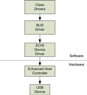
FIGURE 4.19 Software Stack on ECHI Controller.
The EHCI host controller manages the transmission and reception of frames on the bus. The Enhanced USB host controller contains two sets of software accessible hardware registers, memory-mapped registers, and optional PCI configuration registers. The PCI configuration registers are required if the host controller is implemented as a PCI device. The PCI registers contain the PCI header and some additional configuration registers required to allocate the appropriate system resources during enumeration. The PCI registers are not used by the USB driver after enumeration.
The memory-mapped registers are divided into two sections:
• Capability registers are a set of read-only capability registers. The capability registers specify the limits, restrictions, and capabilities of a host controller implementation. These values are used as parameters to the host controller driver.
• Operational registers (which are read/write). The operational registers are used by system software to interact with the operational state of the host controller. The operation registers contain pointers to lists in host memory that are used to define the traffic to be transmitted and received.
Figure 4.20 shows the register structure for a PCI ECHI controller.
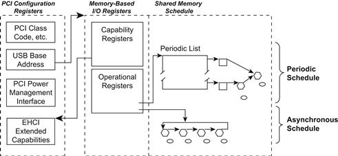
FIGURE 4.20 EHCI Register Classification.
Source: http://www.intel.com/technology/usb/download/ehci-r10.pdf
The EHCI provides support for two categories of transfer types: asynchronous and periodic. Periodic transfer types include both isochronous and interrupt. Asynchronous transfer types include control and bulk. Figure 4.20 illustrates that the EHCI schedule interface provides separate schedules for each category of transfer type. The periodic schedule is based on a time-oriented frame list that represents a sliding window of time of host controller work items. All isochronous and interrupt transfers are serviced via the periodic schedule. The asynchronous schedule is a simple circular list of schedule work items that provides a round-robin service opportunity for all asynchronous transfers.
Note
Wake on USB: The ECHI specification often describes the physical location of the registers within the device. Different parts of the ECHI controller are powered by different supply voltages within the SOC. As a result, some sets of registers retain their values during different CPU power states. These features are provided to support wakeup events from a USB device. Consider the case where your laptop is in a sleep state (suspended); moving the mouse can trigger a wakeup event to the platform, but in order to do so the ECHI controller must remain powered.
The ECHI controller generates interrupts to the processor based on a number of events. One such interrupt is generated at a point in the processing of the asynchronous lists. This is configured when the list is generated by the driver to provide enough advanced notice for the driver to add more work to the list. Another interrupt is generated when the period frame list rolls over; this again is to ensure that the driver supplies data for subsequent frames.
As we mentioned, there are two key lists managed by the driver and consumed by the host controller: the periodic frame list (for isochronous and interrupt traffic) and the asynchronous list (control and bulk transfers). We’ll discuss the asynchronous list first. The list is only processed when the host controller reaches the end of the periodic list, the periodic list is disabled, or the periodic list is empty. That is, it has the lowest priority of all traffic and will only be sent on the bus when there is no other work to do. The asynchronous list is pointed to by a control register: AsyncListAddress. The list is a circular list of queue heads. The controller cycles through each element in the list (in a round-robin fashion), processing each queue head as it goes. One queue head is used to manage the data stream for one endpoint. The queue head consists of a queue element transfer descriptor. The queue head structure contains static endpoint characteristics and capabilities. It also contains a working area from where individual bus transactions for an endpoint are executed. Each queue element transfer descriptor represents one or more bus transactions, which is defined in the context of this specification as a transfer. A descriptor has an array of buffer pointers, which is used to reference the data buffer for a transfer. Figure 4.21 shows how the elements described above are linked together.
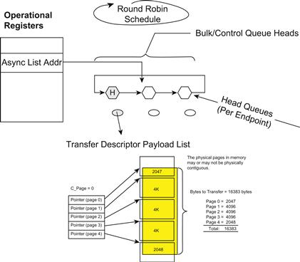
FIGURE 4.21 Async List Address, Head Queues, and Payload Description.
Source: EHCI Intel Spec.
The USB UHCI device driver provides services to the individual class drivers, which make use of the bus drive to transmit and receive data.
Linux Driver
• The Linux USB driver is split into a core and set of class drivers. The core driver provides capabilities to read and write to an endpoint (among other things). The core driver provides a very simple mechanism to access the bus. The steps are as follows (http://lxr.linux.no/linux+v2.6.35.7/drivers/usb/usb-skeleton.c):
• Allocate a USB Request Block (URB) using usb_alloc_urb().
• Copy data into the allocated DMA buffer.
• Initialize the URB with device, endpoint, and data buffer pointers, and a function pointer to a callback routine using the call usb_fill_bulk_urb().
• Submit the URB using usb_submit_urb(). The interface to the USB host controller is asynchronous, which means that the call usb_submit_urb() returns straightaway and does not block to caller.
• The USB driver will call the callback function associated with the URB once the transmission of the data associated with the URB is complete.
That describes the basic mechanism of sending data on the bus, but it is agnostic as to the payload being sent or received. The USB class driver for the device actually formats the payload that sent on the endpoint. For example, a USB pen drive uses the USB mass storage class device driver. Reference source code for the USB mass storage driver can be found at Linux/drivers/usb/storage/.
Device Interconnect—Low Performance
There is a wide range of low-speed, low-pin-count, low-performance interface types. These are used to control sensors, flash devices, simple LCD displays, and the like. In this section we discuss the following interface types:
• Inter-Integrated Circuit (I2C) bus
• Serial Peripheral Interface (SPI) bus
Inter-Integrated Circuit Bus
One of the most prevalent of these buses is known as the Inter-Integrated Circuit bus, or I2C bus. It was invented by Philips (now NXP) in the 1980s. The specification can be found at http://www.nxp.com/documents/user_manual/UM10204.pdf.
The bus standard allows for multiple masters on the bus (however, in many use cases it runs as a single master with multiple slaves attached). It is a simple two-wire bus consisting of a serial clock line (SCL) and a serial data line (SDA). Figure 4.22 shows the interconnection between devices on an I2C bus.
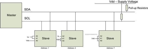
FIGURE 4.22 Single Master I2C Bus.
Each wire (SDA and SCL) is bidirectional. They are driven by open collector gates on each of the devices. Open collector gates allow any device to bring a pin to zero. You may have noticed the pull-up resistors in the diagram; these are typical when open collector outputs are used, and they bring the default bus value to Vdd—a logic one. The protocol is quite simple and is often driven by software directly controlling two general-purpose I/O pins. Each device has a 7-bit address so that transactions can be directed to a particular slave device from the master. The addresses are hard-coded by pull-up/pull-down pins on the device such as A[0-2] in Figure 4.22. Although the bus supports up to 112 devices, most devices export a low number of address bits such as 3 bits. The 3 bits that are selected with the board straps form the lower-order address bits of the device. The higher-order address bits (for example, the remaining 4) are assigned to the device type and built in to the device. The result is that you can have up to eight devices of the same type on a bus, as other devices will contain different high-order address bits.
The bus is controlled by the master device. The master device generates the serial clock, controls bus access, and controls the stop and start conditions. The clock speeds are relatively low, from 10 kHz to 100 kHz and 400 kHz to 2 MHz. The bus follows the following state transitions:
• Bus Not Busy – When both SDA and SCL are high (logic one).
• Start Bus Transfer – A high to low transition of SDA while SCL is high. All commands must start with a start transfer signal.
• Data Transfer – The data line must be set to the required value when the SCL line is low; when the SDL line is high, the data line value is considered to be valid.
• The first byte of data transfer after the start bus transfer consists of 7 bits of slave address and 1 read/write bit to indicate the type of transfer.
• An acknowledge bit/cycle is required after every byte; generally, the slave addressed will generate an acknowledge cycle. This allows the slave to indicate it has accepted the byte. The master releases the SDA line during the acknowledge clock pulse so the slave can pull the SDA line low; it must remain low during the high period of this clock pulse (still generated by the master). If the SDA line remains high during this clock phase, it is treated as a not acknowledge (NACK).
• Stop Bus Transfer – A low to high transition of SDA while SDL is high indicates that the bus transfer has completed, and the bus returns to Not busy.
The format of the data after the address transfer (first byte after a start bus transfer) is dictated by the actual device you connect, for example, a serial EEPROM (http://ww1.microchip.com/downloads/en/devicedoc/21189f.pdf). To perform a byte write to the device, the two bytes following in the device address specify an address to write within the device, and the following byte is the byte we wish to write to the address within the device. Read in the device can take two forms; the first is a current address read capability. The device has an address counter that starts at zero. Each read of the device provides a byte back to the master and the counter is incremented. This is the easiest way to read out the EEPROM contents. There is also an address specific read, but this is accessed by setting the counter using a device write sequence, then reading back the current address value. This is just an example; the actual interactions with the device are defined by the vendor.
System Management Bus (SMBus)
The System Management Bus is a two-wire bus used for host-to-device and device-to-device communications (http://smbus.org/specs/). It was originally invented by Intel, but its principles are similar to that defined by the I2C bus. It is ubiquitous on modern PC motherboards and is used to control the power supply on/off, temperature sensors, fan control, read the configuration from the memory DIMMs, and the like. Intel devices such as the Intel Atom Processor E6xx Series integrate the SMBus host controller, which acts as a master and communicates to slave devices on the motherboard. SMBus specification 2.0 permits a bus speed for an SMBus of between 10 Khz and 100 KHz. The SMBus specification defines a number of commands for use with devices:
• Quick Command – This is the simplest message that can be sent to a device; the only data communicated is the address byte (see I2C) where the read/write bit is only data indication. It can be used to simply turn the device on or off.
• Send Byte – A simple device will recognize its slave address and process the subsequent data byte as a command.
• Receive Byte – Similar to send byte, but gets a data byte from the device. When the device is read it provides a single byte. This could be a temperature reading from a device.
• Write Byte/Word – The first byte of a Write Byte/Word sequence is the command code. The next one or two bytes are the data to be written to the device.
• Read Byte/Word – To read a byte from the device, the host must first write a command to the slave device. Then the host must follow that with repeated START commands to denote a read from the slave; the slave returns one or two bytes of data.
• Process Call – This sends data to the slave device and waits for a response byte based on the data sent to the device.
• Block Read/Write – This is an extension of the read/write byte where a number of bytes to be sent or received is added is indicated after the command byte.
• Block Write-Block Read Process Call – This is an combination of block write and process call: it allows for the transmission of multiple bytes as the “argument” to the process call. The response can also be a variable number of bytes.
The commands described above are all quite similar to the semantics used in an I2C bus, but SMBus has also defined a mechanism for a slave to send a notification to the host (not unlike an I2C slave device becoming the master for a particular transaction). The SMB notification is often used by devices to alert the host processor of a particular condition. For example, an SMBus motherboard temperature sensor could be programmed to generate an alert if the temperature were to go above a critical threshold. In this case, the system software would program the device to send the alert. The system software would not be required to poll the device to check the temperature. However, if the temperature crossed the threshold, the system would be notified. Many devices have a separate alert pin that is asserted to raise a non-maskable or system management interrupt. The system software can generate a broadcast call to read all slave devices that have current alerts active (the address used is the “alert response address”). There are many manufacturers of SMBus devices, such as the Nation Semiconductor LM75. The Linux lm-sensors project provides software that can be used to manage the hardware sensors on an Intel-based motherboard. A comparison between SMBus and I2C can be found in Application note 476, www.maxim-ic.com (direct link does not work).
Serial Peripheral Interface (SPI)
Serial Peripheral Interface (SPI) is a four-wire bus. It consists of a serial clock, master output/slave input, master input/slave output, and a device select pin. The speed of the bus range is much higher than that found in I2C or SMBus; speeds up to 80 MHz are not uncommon. There are variants that provide multiple bits for the transfer (up to 4). These additional data bits dramatically increase the performance. There is no standard specification defined for SPI—it is a de facto standard. The SPI bus is used to connect to serial flash parts that provide the initial boot code for Intel platforms, as shown in Figure 4.23.
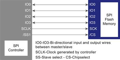
FIGURE 4.23 SPI Interface to Flash Parts.
The effective throughput of a 80-MHz 4-pin serial peripheral interface to a NOR flash device is approximately 40 megabytes per second. This is faster than many parallel interfaces to older NOR flash devices. Intel SOC and chipset integrate SPI host controller, which offloads the processor from driving the SPI protocol on SPI bus.
Audio Buses
Audio buses differ from the low-pin-count buses we have described so far. They typically run continuously, providing audio samples between devices. The most common use case is to connect a codec (analog device with d/a and a/d converters) to a digital SOC where the samples are processed or generated. The Intel-based SOC devices typically use a High Def Audio bus (http://www.intel.com/design/chipsets/hdaudio.htm).
A typical configuration can carry 16 channels per stream, 32-bit audio samples at a sample rate of 192 kHz. The HD audio controller provides DMA engines that manage the transmission and reception of audio samples across the bus with low processor overhead.
Inter IC Sound (I2S)
The I2S bus is another bus defined by Philips (http://www.nxp.com/acrobat_download2/various/I2SBUS.pdf). The bus was designed to transfer audio samples between integrated circuits. The bus is a three-wire bus: a continuously running clock, a data line, and a word select line to allow for the selection of two channels (left/right for stereo), which are time-multiplexed on the data pins.
Universal Asynchronous Receiver/Transmitter
A universal asynchronous receiver/transmitter (UART) is a device that transmits and receives data between a peer UART across a serial line. There are a number of EIA standards, RS-232, RS-422, and RS-485, that define the data format, signals, and electrical voltages on the wires and connector format. The COM port (if it still has one) on PC computer platforms is an RS-232 port. The simplest form of serial communication requires just three wires: a transmit wire, a receive wire, and an electrical ground wire (by which the signals are referenced). To connect two systems together via the serial port, you need to cross over the Tx and Rx wires so the Tx of one port is connected to the Rx of the other port and vice versa. This is known as a null modem cable. There are other wires that can be defined on the serial port connector. There are hardware flow control signals and indications associated with analog modems that are no longer that prevalent. The most standard form is the simple three-wire Tx/Rx and Ground.
A serial port is one of the most basic items you can find on an embedded system. It is quite simple to program and can provide a simple command console and boot indication on when to bring up the system. If the device SOC has a UART, you should definitely make it accessible on your system. In many cases the UART signals are not electrically compatible with the RS-232 standard, and you must use a level shifter to be compatible with an actual RS-232 standard. A Maxim MAX232 is a common level shifter part used to convert the logic levels coming from the UART port to the RS-232 levels.
The asynchronous nature means that there is no separate clock signal to indicate the bit transitions on the Tx and Rx wires. The line encoding used is sufficient for the bits being transmitted to be detected. The transmission consists of a start bit, 5 to 8 data bits, an optional parity bit, and then 1, 1.5, or 2 stop bits. The most ubiquitously used format is No-Parity, 8 data bits, and 1 stop bit. This is usually written as N81.
There are many different speeds supported on UARTS: 300, 600, 1200, 1800, 2400, 4800, 7200, 9600, 14,400, 19,200, 38,400, 57,600, and 115,200 baud. The most common speed used by default on systems is 9600. If the UART is used for heavy data transfer such as downloading images to a platform, a faster baud rate such as 115,200 or higher is used.
When transferring data across the serial port, some form of flow control is often needed. Flow control allows the receiver of the data to indicate to the transmitter than it cannot process additional data sent to it. There are two forms of flow control: hardware and software. The hardware flow control uses additional signal wires (Request to Send and Clear to Send for five-wire RS-232) between the transmitter and receiver to delay the transmission of data to the receiver. More frequently used is software flow control, where the receiver sends a special data value to the transmitter to request that the transmitter pause transmission, and another code to resume the transmission. The characters used are XON/XOFF; XOFF corresponds to the Ctrl-S character and XON corresponds to the Ctrl-Q character. These key sequences can still be used on Linux terminals to pause and resume the terminal.
In some cases, the serial port is used to transfer binary data. In these cases the binary data must be altered and sent in a special format, as it cannot be transmitted directly (imagine XON/XOFF was one of the binary values to be transmitted). A common binary to serial (escaping) format is that provided by a protocol known as kermit (http://www.columbia.edu/Kermit/). Kermit is a terminal emulation program that provides a binary file transfer mechanism. However, the protocol is used more widely than the program itself, especially in embedded systems.
The UART device is a relatively simple device. It provides control registers to set for format (such as N81), clock dividers to set the baud rate, simple transmit and receive FIFOs, and interrupt triggers based on the levels of occupancy within these FIFOs. The model used (register set, behavior, and so on) by the vast majority of UART devices in systems was based on a device known as the 16550A UART, which was originally made by National Semiconductor. There are some limited variations used; one common variation is the size/depth of the FIFO. When the part was originally developed, baud rates supported were relatively low and the size of the corresponding FIFO was quite small; in later revisions or instantiations the FIFO grew to a nominal size of 16 bytes.
The Linux serial driver can be used to start a login shell on a serial port. The serial driver is located in kernel/drivers/serial/8250.c. It supports the 8250 (the 16550A predecessor) and 16550A UART devices. The driver does its best to probe the hardware to identify which variant of UART is there. The serial devices are presented to the system via the /dev/ttyS handle, for example, /dev/ttyS0 for serial port 0 (usually COM port 0 on PCs), /dev/ttyS1 for serial port one, and so on. The Linux boot arguments can specify that a login console be brought up on a specific serial port as follows.
Kernel /vmlinux-2.6.34 ro root=LABEL=/ console=ttyS0,38400
The kernel arguments are specified by the bootloader configuration files. Bootloaders such as Grub, readboot, and uboot all support passing arguments to the kernel.
As the baud rates have increased, there can be some limited performance concerns due to the interaction model with the de facto standard 16550A UART model. In this model the FIFOs must be read by and written to by software byte by byte. In order to reduce the software overheads in handling UARTS, some UART controllers provide a DMA mechanism to transfer the serial characters received from the FIFO to contiguous memory buffers provided by the device driver (similar structure for Transmit). In these cases the interrupt indication is usually based on filling the supplied buffer or a timeout after the last character has been received. This significantly reduces the software overheads associated with transferring data over the serial port. It should be noted that the speeds are still very low in comparison to the relative performance of the processor, and large FIFOs are more common than DMA capable UARTS.
Bluetooth Usage Model
In the previous section we focused on using the UART to interact with a user for debug or a device console provisioning, and so forth. In many platforms the UART is used as a data channel to other devices on the platform. For example, many Bluetooth devices provided a UART interface for connection to the device. For example, the Infineon Bluetooth module (PMB 8763) provides a UART interface Host Controller Interface (HCI) and a Pulse Code Modulation (PCM) interface for audio connections/routing. The HCI transport layer is defined by the Bluetooth organization (www.bluetooth.com). The specification provides for the transmission of commands, events, and data packets between the Host and the Host Controller (Bluetooth device). The specification defines a number of physical interconnects, namely, UART, USB, Secure Digital, and three-wire, that can be used. In many embedded use cases the UART physical interconnect is used, whereas for aftermarket PC designers the USB interface is used. The Bluetooth stack is configured to run over a particular physical interface. There are a number of Linux commands, such as hciattach, hcitool scan, and hcidump, that can be used to discover, attach to, and control Bluetooth devices. The tools are user space tools that communicate with the Bluetooth stack, known as BlueZ (on Linux distributions). You should note that although the UART is a very simple physical interface, a sophisticated multiuse protocol stack can be built on top providing transfer of audio, packet data, contact information, and so on, as shown in Figure 4.24.
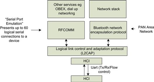
FIGURE 4.24 Bluetooth Protocol Stack.
The Bluetooth air interface can run to several megabits per second (consider a tethered use case where Bluetooth is used to connect to the cell phone, which in turn provides data connectivity at 3G or 4G speeds). As the air interface capabilities have improved, so too must the speed of the UART to connect to Bluetooth radio. As we mentioned above, as the speed increases you may need to make use of DMA features (if they exist) on the UART to reduce the overheads in communicating with the radio.
General-Purpose Input/Output
General-purpose input/output (GPIO) pins are external pins on an SOC device that are under direct control of software. The pins can be typically configured as an input pin or an output pin, or tri-stated.
The value (one or zero) of an output pin is controlled by the value of a specific bit in a control register. In some cases there is also control of the current that the pin can source (called drive strength). The output pin can be connected to any logic device on the platform. A very common use is to tie it to an LED to provide some form of user indication.
There is also a configuration known as open collector. An open collector output can be connected to other open collector outputs from other devices. In this configuration the line is typically pulled up to high with a resistor connected to the supply voltage. In this case any device can drive the line low. This is also known as wired AND for positive TRUE logic.
When the GPIO pin is configured as an input, the logic value on the external pin is reflected in a bit within a register. As the external value changes, it is updated automatically in the register.
In some configurations the input pin logic can be attached to the pin after the output driver so the software can read the actual pin value even though the pin may also be driven by the software. This can be useful for reading the logic state value of an open collector bus, ensuring that the value on the pin reflects the output value, or referencing the value written to output previously. Such feedback logic can also help detect a short on pin or some output contention, where multiple devices are driving different logic values onto the wire (this should not occur but it happens).
It is common to provide some interrupt processing logic that can be assigned to the input pins. An interrupt can typically be generated by the following events on the GPIO pin:
• Active Low Level – This generates an interrupt while the pin signal is low.
• Active High Level – This generates an interrupt while the pin signal is high.
• Rising Edge – This generates an interrupt when the GPIO pin transitions from a low to high signal value.
• Falling Edge – This generates an interrupt when the GPIO pin transitions from a high to low signal value.
• Any Edge – This generates an interrupt when the GPIO pin toggle its states, that is, transitions from a low to high or a high to low signal value.
When controlling the GPIO pins through software, the software will have a number of registers that are memory mapped. Given that the register value may change as a result of change in GPIO pin status, you must ensure that the actual hardware is read. It used to be common to use the C keyword volatile when using pointers to access hardware registers; it is recommended that you use functions supplied by the operating system to read/write to the hardware. These functions ensure that the compiler does not optimize away the access. Figure 4.25 shows a simple example to read a bit value.
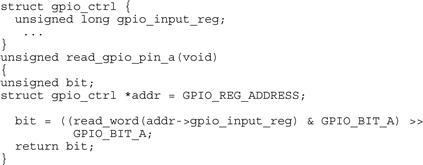
FIGURE 4.25 GPIO Read Pin Example.
A discussion kernel position on volatile can be found in the kernel tree Kernel/Documentation/volatile-considered-harmful.txt.
The I2C bus we described earlier can be implemented using two GPIO pins and a software driver that drives the clock pins and configures the data pin as an output, toggles it in line with the clock output toggles, and then changes the direction of the data pin to an input to receive the data from the bus while continue toggling the clock pin, all through software control.
Power Delivery
The details of the power deliver mechanism are not critical to understand as a software developer, but one topic may be relevant, and that is the management of power failure events. In many cases systems provide an indication that the power is about to fail. In this scenario, the platform has a very limited amount of time to perform critical save operations. The interrupt should be handled with the upmost priority; usually, the software flushes cached elements from RAM to nonvolatile storage (such as flash).
A subset of power fail scenarios is known as brown-outs. These are cases where the power supply drops below its normal operating level but not completely off. Think of an engine cranking in your car; this is such a heavy electrical load that the power to some of the electronics can drop momentarily. Managing these scenarios is beyond the scope of this book, but rest assured there can be significant effort expended in testing these scenario; in particular, the integrity of the nonvolatile storage file systems needs particular attention. The technique often requires fail-safe file system updates that can easily be rolled back in the event of corruption due to brown-outs. It is important to have robust brown-out detection circuitry on such platforms. Bear in mind that nothing can be trusted in this grey zone of operation.
Summary
As you can see, an embedded platform consists of a wide range of peripheral types with many different characteristics. Many of the peripherals we mentioned are now integrated as part of modern SOC devices, while others remain as part of the platform board. We have shown how many of the interfaces are used to expand the capabilities of the SOC device.