Chapter 5
Embedded Processor Architecture
How do we go about classifying an embedded processor? The traditional embedded CPU market is generally divided into microprocessors, microcontrollers, and digital signal processors. Microcontrollers are typically 8-/16-bit processors with a number of input/output (I/O) peripherals, and they are usually self-sufficient in terms of ROM and RAM. Microprocessors, on the other hand, traditionally comprise a 32-bit processor with a number of onboard peripherals. As the transistor continues its reduction in size every year, it has become more and more cost-effective to develop large-scale System-On-Chip (SOC) devices. The majority of SOCs today contain a 32-bit microprocessor integrated with a broad range of additional capabilities alongside the processor. The ability to expand the capabilities of an SOC by integrating industry standard interfaces is an important attribute of developing embedded systems.
The embedded industry currently uses 8-, 16-, and 32-bit processors, continually evolving the performance and applications supported. As applications have steadily evolved well beyond simple control functions, there is a significant migration to 32-bit microprocessor SOCs, as a result we will focus its attention on 32-bit microprocessor based systems. The capabilities of the processors used in the embedded market have typically lagged behind those found in the mainstream processors’ environments. As embedded applications have become more and more complex, requiring higher performance and using larger data sets, this lag is quickly diminishing.
A number of embedded applications incorporate digital signal processing (DSP) algorithms. Consequently, a number of embedded microprocessors incorporate capabilities that are optimized for DSP algorithms. In this book, we discuss processor extensions that are designed to support DSP operations (Chapter 11), but coverage of discrete digital signal processor devices is beyond the scope of this work.
This chapter covers a range of concepts associated with the processor within the SOC, with a focus on topics that are of particular interest when developing embedded systems. Where examples are required we make reference to the Intel® Atom™ processor, and where appropriate make comparisons to other embedded processor architectures.
Basic Execution Environment
All processors provide a register set for use by the programmer. We consider a subset of the registers in a processor to be architecturally defined. Architecturally defined registers are persistent across many specific implementations and generations of the architecture.
All processors provide a general-purpose register file—these registers hold the data to be operated on by the processor. Processors provide a rich set of instructors to operate on these registers; the most basic functions that can be performed are loading to and from memory and logical and arithmetic operations.
The register file on some processors such as ARM™ and PowerPC™ is completely generalized, and most registers can be used as source or destination operators in any of the instructions, whereas other processors impose limitations on the registers that can be used in a subset of the instructions.
The Intel processors provide eight general-purpose registers and six segment registers. The general-purpose registers are known as EAX, EBX, ECX, EDX, ESI, EDI, EBP, and ESP. Although all registers are considered general purpose, some instructions are limited to act on a subset of the registers.
The general-purpose registers are either 32 bits or 64 bits wide, 32 bits when the CPU is configured in IA32 mode and 64 bits in EM64T mode. We will concentrate on 32-bit operation in this chapter, as at the time of writing it is the most widely deployed configuration for Atom-based processors. On Intel processors, naming conventions are used to access the registers in 16- and 8-bit modes. The naming conventions used by mnemonics to access portions of the 32-bit register are shown in Figure 5.1.

FIGURE 5.1 Intel Architecture Register Naming in 32-Bit Mode.
Each processor architecture and programming language has conventions that assign specific uses for particular registers. The general-purpose registers can attain a specific meaning for many reasons, perhaps because the operation is particularly fast with the designated register or more commonly through conventions established by high-level languages. Conventions established by high-level languages are known as application binary interfaces (ABIs). The ABI is a specification (sometimes de facto) that describes which registers are used to pass function variables, manage the software stack, and return values. The ABIs are always architecture specific and often also operating system dependent. As an embedded systems programmer, it’s quite beneficial to know these conventions for your target architecture/operating system/language combination. We describe ABIs in more detail in the section “Application Binary Interface” later in this chapter.
The segment registers on Intel architecture processors are worth a brief discussion. Both the Intel architecture and the operating systems that run on it have evolved over many years. This evolution has allowed the Intel architecture to keep pace with advances in software architectures and best in class operating system design, moving from 16-bit single-thread real-memory models under MS-DOS to multi-threaded protected mode 32- and 64-bit applications under a variety of modern operating system kernels, such as Linux. Features such as segmented memory solved the need of 16-bit applications to access more memory than a single 16-bit register could address. Segment registers were first introduced to allow the generation of a linear address greater than 16 bits. The segment register was shifted and added to a 16-bit register to generate a logical address greater than 16 bits. Intel processors provide three primary modes of operation, namely, Flat, Segmented, and Real 8086 modes. However, today the predominant configuration mode of the processor is the Flat Memory mode. In this mode a selection of bits within the segment registers provide indexes into a table, which selects a segment descriptor. The segment descriptor then provides a base address for the segment. The base address is added to the contents of the register to create the linear address for the memory reference. The segment base addresses are configured by the operating system; they are set to zero for Linux User Space, Linux™ kernel space, and VxWorks™. Some operating systems (such as Linux) use the FS and GS segment registers to access application thread-specific data or OS-specific data in the kernel. The GCC compiler may use GS to implement a runtime stack protector or as a base pointer for Thread Local Storage (TLS).
The key point is that for most Intel environments today you don’t have to worry about the segmentation model to any great extent, as most environments have migrated to a linear 32-bit flat memory model.
In addition to the general-purpose register file, the processor maintains an instruction pointer, flags, stack, and frame pointers:
• Instruction pointer. All processors provide a register that contains the current instruction pointer. The instruction counter is mostly maintained by the processor and updated automatically as the processor executes instructions. The program flow may be altered from its normally increasing (words) sequence through call, branch, conditional instructions, exceptions, or interrupts. On some architecture such as ARM, instructions are provided to directly alter the instruction pointer itself.
• The instruction pointer on Intel architecture is called the Extended Instruction Pointer (EIP). The EIP is a 32-bit register unless the processor is in one of its extended 64-bit modes. There are no instructions that can be used to directly read or write to the EIP. The EIP can only be modified using instructions such as JMP (jump to an address), JMPcc (conditionally jump to an address), CALL (call a procedure), RET (return from a procedure), and IRET (return from an interrupt or exception).
• Flags. All processors provide a register that contain a set of flags. The bits within a flag register on a processor can usually be broken down into two groups. The first are status flags. Status flags are updated as a result of an instruction that operates on one of the general-purpose registers. Examples of instructions that update the status flags are ADD, SUB, and MUL. Status flags can be used by subsequent instructions to change the flow of the program, for example, to branch to a new program address if the zero flag bit is set. Most processors offer a similar set of status flags, sometimes known as condition codes. Intel processors provide the following status flags: Carry, Parity, BCD Carry/Borrow, Zero, Sign, and Overflow.
• Along with the status flags, processors usually have a number of additional bits providing information to the programmer and operating system; these bits are usually specific to the processor architecture. They typically provide information on the privilege level of the processor, a global mask for interrupts, and other bits used to control the behavior of the processor for debugging, legacy support, and so on. The full list of flags in the EFLAGS register is shown in Figure 5.2.
• Stack pointer. In higher-level languages such as C, The program stacks are created in system memory. The stack can used to store local variables, allocate storage, and pass function arguments. It is typical for processors to provide dedicated registers to hold the stack pointer and specific instructions to manipulate the stack. The Intel processor provides PUSH and POP instructions, which operate on the ESP register. Depending on the processor architecture, stacks grow up or grow down as entries are added; which way they grow is a largely arbitrary and up to the architecture creators. In Intel processors, the stack frame grows down.
• Base pointer. In conjunction with the stack pointer, higher-level languages create what’s often known as a stack frame. The base pointer allows the program to manage the function calling hierarchy on the stack. Using a memory dump of the program stack, the base pointer, and stack pointer, you can identify the calling sequence of function calls that occurred before the current function. Some processors provide a dedicated base register, and others just define a specific register by ABI convention. The Intel processor ABIs designate the EBP register as the base pointer. The base pointer is also referred to as a frame pointer in other architectures.
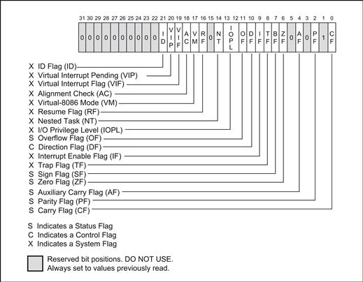
FIGURE 5.2 Intel Architecture EFLAGS Register.
Figure 5.3 brings together the basic view described above and adds some conventions for registers use cases.
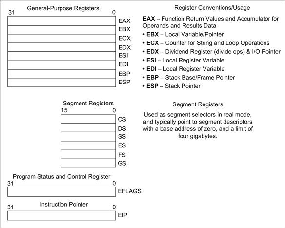
FIGURE 5.3 Basic 32-Bit Execution Environment.
Privilege Levels
All modern embedded processors provide a mechanism to allow portions of the software to operate with differing levels of privilege. The current privilege level is used by the system to control access to resources and execution of certain instructions. The number and specific use of privilege levels are architecture specific, but most architectures support a minimum of two privilege levels. The highest privilege level is usually reserved for the operating system. User programs and applications typically run with a lower privilege level. The use of privilege levels increases the robustness of the system by reducing the ability of an application to interfere with system-wide resources. For example, the ability to disable interrupts is a privileged instruction and ideally not accessible directly by an application.
Intel processors provide four privilege levels, although in practice level zero and level three are predominantly used. The current privilege level (CPL) of the processor is stored in the lowest 2 bits of the code segment selector (CS). The highest privilege level is number zero. This level is commonly known as Kernel Mode for Linux and Ring 0 for Windows-based operating systems. A CPL of three is used for user space programs in both Linux and Windows.
Many processors simply grant privileges to execute system level instructions or access system level resources by being at a privileged supervisor level. However, on Intel architecture processors some further details are required to understand how an Intel processor decides whether an operation is allowed. Whether an instruction has sufficient privilege to perform a specific operation is established by comparing the CPL to the active I/O Privilege Level (IOPL) The IOPL is stored in bits 12 and 13 of the FLAGS register and its value is controlled by the operating system. If the CPL is less than the current IOPL, then the privileged operation is allowed; if greater than or equal to IOPL, then a privileged operation will fail. On an Intel processor the CPL value is stored in the low 2 bits of the Code Segment register. Most operating systems set the IOPL value to three, thus having a CPL value of three corresponds to the lowest privilege level allowed in the system, and a CPL value of zero is the highest privilege level. As an embedded systems programmer, you might often require direct access to a hardware resource from your application. Most operating systems provide a mechanism to alter the privilege level, and a root privileged application, for example, can call the IOPL() function on Linux to altar the IOPL flags. To increase the security of your application you should minimize the time where the code executes with higher privilege level, and you should not run the entire application with increased privileges.
Floating-Point Units
Floating-point mathematical operations are required in a wide range of embedded applications, such as control systems and digital signal analysis. Where an application does require floating point, the performance targets often dictate the need for a hardware-based floating-point unit. Most embedded processor SOCs offer a version that provides hardware-based floating point. A key attribute of a floating point acceleration function associated with the processor is whether the floating-point unit is compliant with the IEEE Standard 754 for Binary Floating-Point Arithmetic. The precision of the floating-point unit (single/double) is also an important attribute in developing the floating-point algorithms.
Intel processors have two floating-point units. The first and probably best known is the x87 Floating-Point Unit (FPU). The x87 FPU instructions operate on floating-point, integer, and binary-coded decimal (BCD) operands. It supports 80-bit precision, double extended floating-point. The FPU operates as a coprocessor to the instruction unit. The FPU instructions are submitted to the FPU and the scalar (main processor) pipeline continues to run in parallel. To maximize overall application performance it is important to ensure that the processor’s main execution flow can perform useful work while the FPU performs the floating-point operations. To that end it is usually best to use a compiler to generate the target code to ensure efficient instruction scheduling.
Not all floating-point operations can be completed; for example, dividing a number by zero results in a floating-point fault. The following floating-point operations result in faults: all invalid operations, for example, square root of a negative number, overflow, underflow, and inexact result. The operating system provides an exception handler to handle the floating-point fault exceptions. In the case of Linux, the kernel catches the fault and sends a user space signal (SIGFPE, signal floating-point exception). The application will be terminated unless the application has chosen to handle the exceptions. The C language specification as defined by the ISO C99 (ISO/IEC 9899:1999) standardizes a number of functions to control the behavior of floating-point rounding and exception handling. One such function is fegetexceptflag().
Intel processors also have a Single Instruction Multiple Data (SIMD) execution engine. The Intel Atom processor supports the Supplemental Streaming SIMD Extensions 3 (SSSE3) version of the SIMD instructions, which support integer, single, and double precession floating-point units.
The Intel Atom processor has a rich set of floating-point coprocessor capabilities. As a result, a particular algorithm could be implemented in a number of ways. The trade-offs for the use of each floating-point unit for a particular operation are described in Chapter 11, “Digital Signal Processing.”
The floating-point units are resources that contain a number of registers and some current state information. When different software threads wish to use the resources, the kernel software may have to save and restore the registers and all state information during operating system context switches. The Intel processor provides FXSAVE and FXRSTOR to save and restore the required state and register information of FP and SSE units. These operations can be costly if performed on every task transition, so Intel processors provide a mechanism to help the kernel identify whether an FPU was actually used by a particular process. The TS flag in the control register zero (CS0.TS) provides an indication that the floating point unit has been used. The kernel can clear the value when it performs a context switch, and check if the bit has been set during the execution of the process (indicating the process used the FP unit). The operating system can be configured to save the registers and state on transition from a thread that used the resource or alternatively raise an exception when a new thread attempts to use the resource after a previous thread has used it. If the real-time behavior of your FP/SSE code is important, you should look into the detailed operating system behavior. You may have to take special steps if you want to use floating-point or SSE units from within the kernel. For example, in Linux you have to call kernel_fpu_begin() and kernel_fpu_end() around the code that uses the FP/SSE units. This will save and restore the required state.
Processor Specifics
Practically all embedded processors have been in existence for a number of generations, though none of the existing embedded processors quite match the longevity of the Intel architecture. As each product generation evolves, new capabilities are introduced, and as an embedded systems developer you will need to establish exactly which features are supported on the particular version you are working with. Having mechanisms to identity product capabilities at runtime facilitates the development of code that will run on a number of different generations of the part without modification. The information is typically provided by special registers that are accessed via dedicated instructions. For example, on ARM platforms, there are a number of co-processor registers one of which is the System Control co-Processor. The system control coprocessor is known as CP15 and provides information and controls the processor behavior. On Intel platforms, a number of control/information registers, CR0, CR1, CR2, CR3, and CR4, and a special instruction (CPUID) are available. The CPUID instruction and registers describe capabilities of the processor and also provide some current processor state information. The CPUID instruction provides detailed information on the executing processor. The output from the CPUID instruction is dependent upon the contents of the EAX register; by placing different values in the EAX register and then executing the CPUID instruction, the CPUID instruction performs the function defined by the EAX value. The CPUID instruction returns the requested values in the EAX/EBX/EDX and ECX registers. The code segment below uses GCC compiler inline assembly code to dump all the CPUID values available on an Intel Atom platform.
long maxCpuId=0 , long cpuid;
long eax = 0, ebx = 0, ecx=0, edx=0;
eax = 0; /∗ Get the maximum CPUID range ∗/
/∗
∗ Input:Loads eax input register with eax variable value
∗ Call CPUID instrucion
∗ Output:Ensure EAX/EBX/EXC and EDX registers are mapped
∗ the variables with the corresponding name.
∗/
__asm__ __volatile__
("CPUID"
:"=a"(eax), "=b"(ebx), "=c"(ecx), "=d"(edx)
:"a"(eax)
);
maxCpuId=eax; /∗ Get the maximum value for EAX∗/
for ( cpuid=0; cpuid <= maxCpuId ; ++cpuid)
{
eax = cpuid;
__asm__ __volatile__("CPUID"
:"=a"(eax), "=b"(ebx), "=c"(ecx), "=d"(edx)
:"a"(eax)
);
printf("CPUID [%2X] = %08X, %08X, %08X, %08X ",cpuid, eax,ebx,ecx,edx);
}
The code above displays the various CPUID values, which can be decoded to provide detailed information about the processor. A good example of the type of information provided is the processor feature list. This is provided by calling CPUID with an EAX value of 01h. The processor features capabilities listed on an Atom processor returned the following values: EDX[31:0] = 0xBFE9FBFF and ECX[31:0] = 0x0040C3BD. Decoding the bits set in EDX/ECX indicates the following feature set on the Intel Atom processor: Floating-Point Unit, Time Stamp Counter, Physical Address Extension, Local Interrupt Controller (APIC), Cache Line Flush, Model Specific Registers, FXSAVE/FXSTOR, MMX, SSE, SSE2, SSE3, SSSE3, Thermal Management, Multi-Threading – (Hyper thread). The support for 64-bit operation (EM64T) is also indicated through the CPUID feature.
It is often useful to have an awareness of the cache structures on your platform, especially when it comes to performance tuning or at least understanding the behavior of your application and the correlation between application data set size and overall cache sizes. Chapter 18, “Platform Tuning,” provides more specific details on tuning your system. The CPUID provides cache structure details of the processor. The decoded values returned from the current Intel Atom processor are as follows:
• L1 data cache: 24 kB, six-way set associative.
The Linux command cat/proc/cpuinfo provides similar details relating to the CPU. A portion of the details presented is obtained by issuing using the CPUID instruction.
The provision of free running counters and hardware timers is required by most operating systems to provide the operating system “Tick,” timed delay loops, code performance measurements, and the like. Intel Atom platforms provide a wealth of timers and counters on the platform. A very useful free running time stamp counter is provided on Intel platforms. It is simply accessed by using the RDTSC instruction. The instruction returns the number of ticks at maximum processor frequency (resolved at boot up) since reset. The tick represents the length of time for one duty cycle of the CPU clock, so for a processor running at 1.6 GHz, a tick would represent 0.625 ns. The value is very reliable, but you should be aware that in some system interactions may skew some measurements, such as when the processor’s actual speed is slowed due to power-managed controls, although this is not the case for Atom processors. The code segment below shows how the time stamp counter can be read from a C program. The embedded assembly is written to be compiled by the GCC compiler.
long long timeStamp;
__asm__ __volatile__
("RDTSC" ; Mnemonic to read counter
:"=A"(timeStamp) ; Map 64bit timeStamp to EDX/EAX
:
);
In addition to the free running counter, embedded platforms will make use of hardware-based timers. The timers on the Intel Atom platform are described in Chapter 4, “Embedded Platform Architecture.”
Application Binary Interface
As an embedded software developer, you will develop most of your software in higher-level languages. It is less likely that you have to develop large portions of your code in assembly language. However, it is very important that you are conversant with assembly language and how assembly and high-level languages interact, particularly when it comes to debugging the platform. For embedded systems it is not unusual to have to “root cause” a system crash with information saved at the time of the system crash. A common example of this is debugging Linux Kernel Oops (http://www.kerneloops.org). The crash logs provide register values, stack frames, and software versions at the time of the crash. Understanding the register usages and calling convention of the high-level language is critical to debugging such logs. There is little formal standardization of the calling conventions but in general two de facto standard conventions predominate. The open source Gnu Compiler (GCC) conventions are used on Unix-like operating systems and most real-time operating systems, whereas the Microsoft Compiler calling conventions are used by compilers and tool chains on Windows-based operating systems. The best source of information on Linux/Unix type ABIs is located at http://refspecsfreestandards.org; consult http://msdn.microsoft.com for Windows-based platforms. As an indication of the fragmentation that arises, the Intel C++ Compiler provides an -fabi-version option, which allows you to select between most recent ABI, g++ 3.2 and 3.3 compatible, or compatible with gcc 3.4 and higher.
The calling conventions define the following aspects of the code generated by compilation:
The width (number of bits to represent) of data types is largely standard across all compilers and in general is intuitive. The alignment and packing behavior, on the other hand, can vary significantly and cause difficulty when debugging the stack trace associated with a crash. In general, data types are aligned to the width of the data type. A 4-byte integer is aligned to a 32-bit address; this is also known as double word aligned. The number of bits in a word, double word, and quad word is itself a convention specific to the processor architecture. On IA-32 processors, a 16-bit value is a word, a 32-bit value is a double word, and a 64-bit value is a quad-word. ARM and PowerPC architectures were defined later and word size changed to 32 bits, therefore making 16-bit values half words and 64-bit values double words.
The compilers also provide compiler options and pragmas that can be used to change the alignment of basic types and structure members. The most common option to change the way elements in a structure are aligned is the __PACKED__ pragma or equivalent command line compiler option. In this case all members of a structure are packed together, leaving no unused memory space. The alignment of members may not be on their natural boundary. This mechanism is often used in embedded systems where we want to share information between different systems or overlay a structure over the register map of a device. When sharing information across processors within a system or between systems, this approach may suffice, but it is not very rigorous. When sharing data across embedded systems, it is important to format the data in a formally agreed-upon standard for transmission; this removes all packing and endian issues that may arise. Common packing standards are eXternal Data Representation (XDR) and, more recently, XML.
The stack alignment is typically double word (4-byte) aligned for 32-bit operating systems and 16-byte aligned for 64-bit operating systems. The compiler will often have an option to set the alignment. An example of such an option is -mpreferred-stack-boundary=value , which is available when using a GCC compiler. The alignment of the stack is useful to know when debugging stack traces.
The processor’s register usage by high-level languages can be divided into a number of categories:
• Caller saved registers. A number of registers may be altered (such as scratch registers) when a function is called; if the caller needs to retain this value, the caller must save the contents of these registers on the stack to facilitate restoration after the function returns.
• Callee saved registers. This is the list of registers the called function must restore to their previous value when the function returns.
• Function argument passing registers. Arguments are passed to a function either in registers or on the stack, depending on the number and type of arguments. For 32-bit IA-32 ABIs, all function parameters are passed on the stack; for 64-bit ABIs, a combination of registers and stack is used.
• Function return value registers. Function that returns a value does so in a register.
The IA-32 registers for the GNU compiler Linux 32-bit ABI are shown in Table 5.1. At the time of writing, a new draft ABI for use on Intel EM64T-capable processors is known as X32-ABI (https://sites.google.com/site/x32abi/). It maximizes the use of the registers available while enabled in EM64T mode, yet retains pointer, long, and integer sizes as if it were a 32-bit machine. This is a best-case hybrid for 32-bit applications.
Table 5.1. ABI Register Calling Conventions—32-Bit Linux/Windows
| IA-32 Register | 32-Bit Linux GNU/Windows |
| EAX | Scratch and return value |
| EBX | Callee save |
| ECX | Scratch |
| EDX | Scratch and return value |
| ST0-ST7 | Scratch/ST0 return float |
| ESI | Callee save |
| EDI | Callee save |
| EBP | Callee save |
| XMM0-XMM7 | Scratch registers |
| YMM0-YMM7 | Scratch registers—256 bit on AVX-capable processors only |
A key aspect of the calling conventions is the creation of a stack. The stack is built up from a number of stack frames. Each stack frame consists of memory that is allocated from the program stack. The stack frame consists of parameters to the function being called, automatic stack variables, saved scratch registers, and callee and caller saved register values. A number of conventions specify where the stack cleanup operations must take place. These are known as cdecl, stdcall, and fastcall. The cdecl is the default calling convention and requires the calling function to perform the stack cleanup. The cdecl calling convention supports functions with a variable number of arguments such as printf. The stdcall calling convention supports a fixed number of arguments for a function and the stack cleanup is performed by the called function. The majority of embedded systems use the C default cdecl convention. Windows libraries primarily use the stdcall convention. The fastcall convention is an additional convention supported by Linux and Windows to increase the performance of the function call. It is critical that the caller and callee use the same convention—if not, the stack program will undoubtedly crash.
The following sequence of actions is performed as part of a function call:
• Save scratch registers in the caller.
• Push the function arguments onto the stack from right to left.
• Call the function, and the call instruction pushes the Instruction Pointer (EIP) onto the stack and transfers control to the function. The EIP value contains the address of the next instruction, and therefore the stack will contain the address of the instruction after the call.
• Save the base pointer (pushed onto the stack) and update the base pointer with the current stack pointer. The base pointer can now be used to reference the calling arguments. The first argument of the function is referred to by 8(%EBP); the second argument is accessed by 12(%EBP).
• Save scratch registers (caller save) used by this function.
• Grow the stack for local variables, simply by decrementing the ESP by the amount of space needed. Local variables are typically accessed by relative reference from the EBP.
• Free the local stack storage, by adding the appropriate value to the ESP.
• Restore the scratch registers.
• Restore the base pointer, using POP.
• Return from the function, using RET. This moves the previously pushed address off the stack and transfers control to the instruction after the call.
• As this is the cdecl convention, the caller now frees the stack of the calling arguments, typically discarded by adding the required value to the ESP, or if the variables are reused, the values are moved into registers with POP for reuse.
The following section shows a simple C function call and the corresponding assembly.
main()
{
int a = 1; x = 100; y = 150;
int z;
z = foo1(a,x,y);
printf("Z foo1:%d ", z);
}
int foo1(int a, int x, int y)
{
int z;
z = a + x + y;
return(z);
}
This produces the following assembly code using GNU disassembly format. The code is produced by calling gcc with the –S option. The GNU tools command objdump (called with argument –s) is very useful command in studying study the assembly code of an object or executable.
1 main:pushl %ebp ; Save the base pointer
2 movl %esp, %ebp ; Set the stack = base
3 andl $-16, %esp ; Allocate stack -16
4 subl $32, %esp ; Allocate stack -32
5 movl $1, 16(%esp) ; Put 01h into variable a
6 movl $100, 20(%esp) ; Put 100h into variable x
7 movl $150, 24(%esp) ; Put 100h into variable y
8 movl 24(%esp), %eax ; Get y into eax
9 movl %eax, 8(%esp) ; Put y onto stack
10 movl 20(%esp), %eax ; Put x into eax
11 movl %eax, 4(%esp) ; Put x onto stack
12 movl 16(%esp), %eax ; Put a into eax
13 movl %eax, (%esp) ; Push a onto stack
14 call foo1 ; Call the function
15 movl %eax, 28(%esp) ; Put return z onto local stack
16 movl 28(%esp), %eax ; Move local variable into eax
17 movl %eax, 4(%esp) ; move return z into call stack
18 movl $.LC0, (%esp) ; move pointer to printf str
20 leave ; Set ESP to EBP, POP EBP
21 ret ; return from function.
22 …
23 foo1:
24 pushl %ebp ; Save the base pointer
25 movl %esp, %ebp ; Set the stack = base
26 subl $16, %esp ; Grow stack by 16 bytes
27 movl 12(%ebp), %eax ; Get x from stack into eax
28 movl 8(%ebp), %edx ; Get a from stack into edx
29 leal (%edx,%eax), %eax ; Add edx+eax into eax
30 addl 16(%ebp), %eax ; add y to eax
31 movl %eax, -4(%ebp) ; put Z local regstack
32 movl -4(%ebp), %eax ; put local Z into return reg
33 leave ; Sets ESP to EBP and POPs EBP
34 ret ; Return from function
35
36 .section .rodata
37 .LC0:
38 .string "Z foo1:%d " ; String for printf
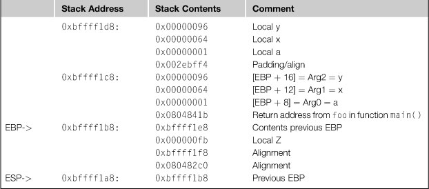
The stack dump below in Table 5.2 is a snapshot of the stack when the processor is executing from line 32 above. The table shows the different stack values, parameters, local variables, and return addresses.
Table 5.2. Detailed Example Stack Snapshot
The code generated for this simple function is far from optimized, and was generated with the default compiler options. The instruction count for the function foo() above is 11 instructions, with the average optimization (GCC option –O2), the code generated is reduced to 7 instructions. The optimized code will make more efficient usage of the stack as well.
Processor Instruction Classes
In this section, we outline the general classes of instructions available in most processors. This is by no means a complete list of instructions; the goal is to provide a flavor of the instruction classes available. As an embedded programmer, this is often the level of detail you will require; you should be familiar enough to read assembly code, but not necessarily proficient at writing highly optimized large scale assembly.
First, a brief segway to discuss the symbolic representation of instructions. The actual representation is defined by the assembler used, but not all assemblers use the same presentation for instructions. In the context of this book, the following representation is used:
label: mnemonic argument1, argument2, argument3
• Label is an identifier that is followed by a colon.
• A mnemonic is a reserved name for a class of instruction op-codes that have the same function.
• The operands argument1, argument2, and argument3 are optional. There may be zero to three operands, depending on the op-code. When present, they take the form of either literals or identifiers for data items. Operand identifiers either are reserved names of registers or are assumed to be assigned to data items declared in another part of the program.
When two operands are present in an arithmetic or logical instruction, the right operand is the source and the left operand is the destination (same order as the mathematical assignment operator (=)). For example:
LOADREG: MOV EAX, SUBTOTAL
In this example, LOADREG is a label, MOV is the mnemonic identifier of an op-code, EAX is the destination operand, and SUBTOTAL is the source operand. The direction of the assignment is just a convention set out by the assembler. We’ll call the convention above the Intel convention; the opposite assignment is also used on Intel platforms and it’s known as the AT&T convention. The LOADREG instruction would be shown as follows:
LOADREG: MOV SUBTOTAL, EAX
The Intel Compiler and Microsoft compilers use the Intel convention. The GNU tool chain (including debuggers) uses the AT&T convention by default. However, we use the Intel convention throughout this book, unless it’s an example segment to be used by a GNU tool chain.
The types and number of operand supported by a processor instruction set are architecture specific; all architectures allow operands that represent an immediate value, a register, or memory location. Intel architecture machine instructions operate on zero or more operands. Operands are specified explicitly and others are implicit. The data for a source operand can be found in one of the following:
• The instruction itself (an immediate operand)—The number of bits available in the op-code for an immediate value depends on the processor architecture; on Intel processors an immediate value has a range of 232. RISC processors such as ARM have a fixed size op-code and as a result support immediate values with a reduced range of 216. As a result, RISC processors generally use literal pools to load 32-bit values into a register.
• An I/O port—The Intel architecture supports 64K 8-bit I/O ports that can be written to and read from using the OUT/IN instructions. These ports are now mostly used to provide simple debug output on Intel reference platforms; most will provide a two-character eight-segment LED display to show the values written to I/O PORT 80h and 84h.
When an instruction returns data to a destination operand, it can be returned to:
• Memory location—In limited cases the Intel processor supports direct memory to memory moves, this is typically not supported on RISC processors.
The size of the instruction is worth a brief mention. Most RISC processors such as ARM and PowerPC use fixed size instructions, typically 32-bit instruction word. The Intel processors use variable sized op-codes ranging from a single byte op-code to a theoretical maximum of 17 bytes. When using a debugger to display the raw assembly of a program, the address provided to the decode command must be aligned to an instruction boundary. This can take some practice, although it is pretty obvious when you get it wrong, as the command will display quite a few invalid op-codes.
Immediate Operands
Some instructions use data encoded in the instruction itself as a source operand. The operands are called immediate operands. For example, the following instruction loads the EAX register with zero.
MOV EAX, 00
The maximum value of an immediate operand varies among instructions, but it can never be greater than 232. The maximum size of an immediate on RISC architecture is much lower; for example, on the ARM architecture the maximum size of an immediate is 12 bits as the instruction size is fixed at 32 bits. The concept of a literal pool is commonly used on RISC processors to get around this limitation. In this case the 32-bit value to be stored into a register is a data value held as part of the code section (in an area set aside for literals, often at the end of the object file). The RISC instruction loads the register with a load program counter relative operation to read the 32-bit data value into the register.
Register Operands
Source and destination operands can be any of the follow registers depending on the instruction being executed:
• 32-bit general purpose registers (EAX, EBC, ECX, EDX, ESI, EDI, ESP, or EBP)
• 16-bit general purpose registers (AX, BX, CX, DX, SI, SP, BP)
• 8-bit general-purpose registers (AH, BH, CH, DH, AL, BL, CL, DL)
• System Table registers (such as the Interrupt Descriptor Table register)
On RISC embedded processors, there are generally fewer limitations in the registers that can be used by instructions. IA-32 often reduces the registers that can be used as operands for certain instructions.
Memory Operands
Source and destination operands in memory are referenced by means of a segment selector and an offset. On embedded operating systems, the segment selector often results in a base address of zero, particularly if virtual memory is used, so the memory address specified by the operand degenerates to being the offset value. The segment selector is automatically chosen by the processor, but can be overridden if needed. The following instruction moves the value in EAX to the address pointed by EBX, assuming the data segment selector contains zero. It is the simplest memory operand form.
MOV [EBX], EAX
The memory operand can also specify offsets to the base address specified in the memory operand. The offset is added to the base address (the general-purpose register) and can be made up from one or more of the following components:
• Displacement—An 8-, 16-, or 32-bit immediate value.
• Index—A value in a general-purpose register.
• Scale factor—A value of 2, 4, or 8 that is multiplied by the index value.
So we have a memory operand that can consist of
![]()
Since the segment selector usually returns zero, the memory operand effective address becomes the following:
![]()
The compiler will make best use of these modes to de-reference data structures in memory or on the stack. The components of the offsets can be either positive or negative (two’s complement values), providing excellent flexibility in the memory operand address generation.
Data Transfer Instructions
All processes provide instructions to move data between registers, memory, and registers, and in some architectures between memory locations. Table 5.3 shows some instruction combinations.
Table 5.3. Data Transfer Instructions
| Instruction Mnemonic | Example | Description |
| MOV | MOV EAX,EBX | Move contents between registers. Note that register may be ALU register, segment register, or control registers such as CR0 |
| MOV | MOVEAX,0abcd00h
MOV EAX,[ EBX -4] |
Load a register from memory. Effect address defined by the addressing modes discussed above |
| MOV | MOV [EBX],EAX | Write register contents to memory |
| MOV | MOV EAX,12345678h | Load an immediate value into a register |
| MOV | MOV EAX,[4∗ESI][EBX+256] | Load memory at 4∗ESI + BX + 256 to register ax |
| MOV | MOVS EDI,ESI | String move memory to memory |
| PUSH | PUSH EBP | Push ECX value onto stack. Update EBP |
| POP | POP ECX | Pop ECX, update EBP |
| XCHG | XCHG EBX, ECX | Swap register values |
| XCHG | XCHG [EAX],EBX | Swap contents at memory location with register value in atomic fashion |
| CMOVcc | CMOVE EAX,[EBX] | Move if Flags show equal (ZF = 1) |
There is also a set of instructions that provides hints to the underlying hardware to help manage the cache more efficiently. The MOVNTI (store double word using non-temporal hint) instruction is designed to minimize cache pollution; by writing a double word to memory without writing to the cache hierarchy, it also prevents allocation in the cache line. There are also PREFETCH instructions that perform memory reads and bring the result data closer to the processor core. The instruction includes a temporal hint to specify how close the data should be brought to it. These instructions are used when you are aggressively tuning your software and require some skill to use effectively. More details are provided in Chapter 18, “Platform Tuning.” These hints are optional; the processor may ignore them.
Arithmetic Instructions
The arithmetic instructions define the set of operations performed by the processor Arithmetic Logic Unit (ALU). The arithmetic instructions are further classified into binary, decimal, logical, shift/rotate, and bit/byte manipulation instructions.
Binary Operations
The binary arithmetic instructions perform basic binary integer computations on byte, word, and double word integers located in memory and/or the general-purpose registers, as described in Table 5.4.
Table 5.4. Binary Arithmetic Operation Instructions
| Instruction Mnemonic |
Example | Description |
| ADD | ADD EAX, EAX | Add the contents of EAX to EAX |
| ADC | ADC EAX, EAX | Add with carry |
| SUB | SUB EAX, 0002h | Subtract the 2 from the register |
| SBB | SBB EBX, 0002h | Subtract with borrow |
| MUL | MUL EBX | Unsigned multiply EAX by EBX; results in EDX:EAX |
| DIV | DIV EBX | Unsigned divide |
| INC | INC [EAX] | Increment value at memory eax by one |
| DEC | DEC EAX | Decrement EAX by one |
| NEG | NEG EAX | Two’s complement negation |
Decimal Operations
The decimal arithmetic instructions perform decimal arithmetic on binary coded decimal (BCD) data, as described in Table 5.5. BCD is not used as much as it has been in the past, but it still remains relevant for some financial and industrial applications.
Table 5.5. Decimal Operation Instructions (Subset)
| Instruction Mnemonic |
Example | Description |
| DAA | ADD EAX, EAX | Decimal adjust after addition |
| DAS | DAS | Decimal adjust AL after subtraction. Adjusts the result of the subtraction of two packed BCD values to create a packed BCD result |
| AAA | AAA | ASCII adjust after addition. Adjusts the sum of two unpacked BCD values to create an unpacked BCD result |
| AAS | AAS | ASCII adjust after subtraction. Adjusts the result of the subtraction of two unpacked BCD values to create a unpacked BCD result |
Logical Operations
The logical instructions perform basic AND, OR, XOR, and NOT logical operations on byte, word, and double word values, as described in Table 5.6.
Table 5.6. Logical Operation Instructions
| Instruction Mnemonic | Example | Description |
| AND | AND EAX, 0ffffh | Performs bitwise logical AND |
| OR | OR EAX, 0fffffff0h | Performs bitwise logical OR |
| XOR | EBX, 0fffffff0h | Performs bitwise logical XOR |
| NOT | NOT [EAX] | Performs bitwise logical NOT |
Shift Rotate Operations
The shift and rotate instructions shift and rotate the bits in word and double word operands. Table 5.7 shows some examples.
Table 5.7. Shift and Rotate Instructions
| Instruction Mnemonic |
Example | Description |
| SAR | SAR EAX, 4h | Shifts arithmetic right |
| SHR | SAL EAX,1 | Shifts logical right |
| SAL/SHL | SAL EAX,1 | Shifts arithmetic left/Shifts logical left |
| SHRD | SHRD EAX, EBX, 4 | Shifts right double |
| SHLD | SHRD EAX, EBX, 4 | Shifts left double |
| ROR | ROR EAX, 4h | Rotates right |
| ROL | ROL EAX, 4h | Rotates left |
| RCR | RCR EAX, 4h | Rotates through carry right |
| RCL | RCL EAX, 4h | Rotates through carry left |
The arithmetic shift operations are often used in power of two arithmetic operations (such a multiply by two), as the instructions are much faster than the equivalent multiply or divide operation.
Bit/Byte Operations
Bit instructions test and modify individual bits in word and double word operands, as described in Table 5.8. Byte instructions set the value of a byte operand to indicate the status of flags in the EFLAGS register.
Table 5.8. Bit/Byte Operation Instructions
| Instruction Mnemonic |
Example | Description |
| BT | BT EAX, 4h | Bit test. Stores selected bit in Carry flag |
| BTS | BTS EAX, 4h | Bit test and set. Stores selected bit in Carry flag and sets the bit |
| BTR | BTS EAX, 4h | Bit test and reset. Stores selected bit in Carry flag and clears the bit |
| BTC | BTS EAX, 4h | Bit test and complement. Stores selected bit in Carry flag and complements the bit |
| BSF | BTS EBX, [EAX] | Bit scan forward. Searches the source operand (second operand) for the least significant set bit (1 bit) |
| BSR | BTR EBX, [EAX] | Bit scan reference. Searches the source operand (second operand) for the most significant set bit (1 bit) |
| SETE/SETZ | SET EAX | Conditional Set byte if equal/Set byte if zero |
| TEST | TEST EAX, 0ffffffffh | Logical compare. Computes the bit-wise logical AND of first operand (source 1 operand) and the second operand (source 2 operand) and sets the SF, ZF, and PF status flags according to the result |
Branch and Control Flow Instructions
We clearly need instructions to control the flow of a program’s execution. The branch and control flow instructions fall into two primary categories. The first is unconditional changes of program flow to a new program counter address. This occurs when a jump or call instruction is encountered. The second category of branch or control flow instructions are conditional branches or conditional execution of an instruction. The conditional execution of an instruction is dictated by the contents of bits within the EFLAGS register, or for some instructions the value in the ECX register.
Jump operations transfer control to a different point in the program stream without recording any return information. The destination operand specifies the address of the instruction we wish to execute next. The operand can be an immediate value, a register, or a memory location. Intel processors have several different jump modes that have evolved over time, but a number of modes are no longer used. The near jump is a jump within the current code segment. As we mentioned earlier, the current code segment often spans the entire linear memory range (such as zero to 4 GB). So all jumps are effective within the current code segment. The target operand specifies either an absolute offset (that is, an offset from the base of the code segment) or a relative offset (a signed displacement relative to the current value of the instruction pointer in the EIP register). A near jump to a relative offset of 8 bits is referred to as a short jump. The CS register is not changed on near and short jumps. An absolute offset is specified indirectly in a general-purpose register or a memory location. Absolute offsets are loaded directly into the EIP register. A relative offset is generally specified as a label in assembly code, but at the machine code level it is encoded as a signed 8-, 16-, or 32-bit immediate value. This value is added to the value in the EIP register. (Here, the EIP register contains the address of the instruction following the JMP instruction). Although this looks complicated, in practice the near jump is a simple branch with flexibility in specifying the target destination address. Intel processors also includes FAR jumps, which allow the program to jump to a different code segment, jump through a call gate with privilege checks, or a task switch (task in the IA-32 processor context). Table 5.9 shows the different instructions with examples.
Table 5.9. Program Flow—No Saved Return State
| Instruction Mnemonic |
Example | Description |
| Jmp | JMP target_label | Jumps unconditionally to the destination address operand |
| JZ | JZ target_label | Jumps conditionally to the destination operand if the EFLAG. Zero bit is set |
| JNZ | JZ target_label | Jumps conditionally to the destination operand if the EFLAG. Zero is not set |
| LOOP | MOV ECX,5
LoopStart: XXX YYY LOOP LoopStart |
Decrements the contents of the ECX register, then tests the register for the loop-termination condition. If the count in the ECX register is non-zero, program control is transferred to the instruction address specified by the destination operand |
Call gates are sometimes used to support calls to operating system services; for instance, this is a configuration available in VxWorks for real-time tasks when calling operating system services. However, operating system calls are more usually provided via the software interrupt call.
Calling subroutines, functions, or procedures require the return address to be saved before the control is transferred to the new address; otherwise, there is no way for the processor to get back from the call. The CALL (call procedure) and RET (return from procedure) instructions allow a jump from one procedure (or subroutine) to another and a subsequent jump back (return) to the calling procedure. The CALL instruction transfers program control from the current procedure (the calling procedure) to another procedure (the called procedure). To allow a subsequent return to the calling procedure, the CALL instruction saves the current contents of the EIP register on the stack before jumping to the called procedure. The EIP register (prior to transferring program control) contains the address of the instruction following the CALL instruction. When this address is pushed on the stack, it is referred to as the return instruction pointer or return address. The address of the called procedure (the address of the first instruction in the procedure being jumped to) is specified in a CALL instruction in the same way it is in a JMP instruction (described above).
Most processors provide an instruction to allow a program to explicitly raise a specified interrupt. The INT instruction can raise any of the processor’s interrupts or exceptions by encoding the vector number or the interrupt or exception in the instruction or exception, which in turn causes the handler routine for the interrupt or exception to be called. This is typically used by user space programs to call operating system services. Table 5.10 shows the instructions that affect the program flow.
Table 5.10. Program Flow with Saved Return State
| Instruction Mnemonic | Example | Description |
| CALL | CALL target_label | Saves the return address of the stack and jumps to subroutine |
| RET | RET | Returns to the instruction after the previous call |
| INT x | INT 13h | Calls software interrupt 13 |
| IRET | IRET | Returns from the interrupt handler |
On Intel platforms there is quite a lot of history associated with the INT calls. Legacy (non-EFI) BIOS supports a number of INT calls to provide support to operating systems. An example of a well-known INT call is the E820. This is an interrupt call that the operating system can use to get a report of the memory map. The data are obtained by calling INT 15h while setting the AX register to E820h. For embedded programmers, there is an ever-decreasing dependence on the INT service provided by the BIOS. The Linux kernel reports the memory map reported by the BIOS in the dmesg logs at startup.
The BIOS environment is transitioning from a traditional legacy BIOS, which was first developed a few decades ago, to a more modern codebase. The newer codebase is known as Unified Extensible Firmware Interface (UEFI). At the time of writing, many products are transitioning from this legacy BIOS to EFI. More information on this topic can be found in Chapter 6.
Structure/Procedure Instructions
Modern languages such as C/C++ define a frame structure on the stack to allocate local variables and define how parameters are passed on the stack. The IA-32 provides two instructions to support the creation and management of these stack frames, namely, ENTER and LEAVE. The stack frame is discussed as part of the Application Binary Interface discussed earlier in this chapter.
SIMD Instructions
Several classes of embedded applications are a mix of traditional general-purpose (scalar) workloads with an additional moderate digital signaling workload. Most embedded processors provide extensions to their core instruction set to support these additional workloads. These instructions are known as Single Instruction Multiple Data (SIMD). On Intel platforms the extensions are known as Intel Streaming SIMD Extensions (Intel SSE). Other processors have more basic extensions to provide single multiply-and-accumulate (MAC) operations. This operation is the basic building block for a large number of simple DSP algorithms. Over time the range of SSE instructions has grown significantly, and in fact they can bring substantial performance benefits to a wide range of workloads:
• Speech compression algorithms and filters
• Speech recognition algorithms
• Video display and capture routines
• Image and video processing algorithms
Generally, code that contains small-sized repetitive loops that operate on sequential arrays of integers of 8, 16, or 32 bits, single-precision 32-bit floating-point data, and double-precision 64-bit floating-point data are a good candidate for tuning using SSE instructions. The repetitiveness of these loops incurs costly application processing time. However, these routines have the potential for increased performance when you convert them to use one of the SIMD technologies.
On the Intel Atom processor, the SSSE3 SIMD instructions are supported and the instructions operate on packed byte, word, and double-word integers, as well as single-precision floating point. A key efficiency of the SIMD instructions is the fact that a single instruction operates on a number of data elements in parallel. If your data structures can be structured to make use of SIMD instructions, significant improvements in performance can be obtained. Figure 5.4 shows a typical SIMD operation.

FIGURE 5.4 Typical SIMD Operation.
The following code sequence is an example of how to get the data into the XMM registers and have the SIMD operation performed. It is written in the Intel Compiler format to incorporate assembly into C code.
1 void add(float ∗a, float ∗b, float ∗c)
2 {
3 __asm {
4 mov eax, a
5 mov edx, b
6 mov ecx, c
7 movaps xmm0, XMMWORD PTR [eax]
8 addps xmm0, XMMWORD PTR [edx]
9 movaps XMMWORD PTR [ecx], xmm0
10 }
11
The first three instructions get pointers for a, b, and c into EAX, EDX, and ECX registers, respectively. The MOVAPS instruction in line 7 above moves four quad-words containing four packed single-precision floating-point values from memory pointed to by EAX (128 bytes) into the XMM0 register. The ADDPS instruction performs a SIMD add of the four packed single-precision floating-point values in XMM0 with the four packed single-precision floating-point values pointed to by the EDX register. The final MOVAPS instruction saves the XMM0 (128-byte contents) to the memory pointed to by the ECX register. This is far more efficient than the traditional scalar equivalent.
Exceptions/Interrupts Model
Integral to all processors is the ability for the processor to handle events that are orthogonal to the execution flow of the program. All modern processors have a well-defined model to signal and prioritize these events. The processor can then change the flow of the executing instructions sequence to handle these events in a deterministic manner. The event is typically handled by transferring execution from the current running task to a special software routine. The software routines are called interrupt or exception handlers. The processor will save sufficient processor state information to allow the processor to return to the currently executing task when the interrupt or exception was raised. The resumption of the interrupts task happens with no loss in program continuity unless the exception is not recoverable or causes the running program to be terminated. To aid in handling exceptions and interrupts, each architecturally defined exception and each interrupt condition requiring special handling by the processor is assigned a unique identification number, called a vector.
Interrupts are divided into two types—hardware and software. Hardware interrupts are typically generated as a result of a peripheral (external to the processor core) that needs attention. Peripherals both within the SOC device and on the platform can raise an interrupt to the processor. The processor then transfers control to the appropriate interrupt handled for the specific device interrupt. The allocation and sharing of interrupt vectors is performed by the operating system. A simple example of a peripheral is a timer block, used to “kick” the operating system timer.
Software interrupts are typically triggered via a dedicated instruction such as INT #vector on Intel processors and SWI on ARM architectures. The execution of a software interrupt instruction causes a context switch to an interrupt handler in a fashion similar to an external hardware interrupt. Software interrupts are most often used as part of a system call. A system call is a call to an operating system kernel in order to execute a specific function that controls a device or executes a privileged instruction. The Linux operating system uses INT 0x80 for service calls.
Interrupts can be classed as maskable or non-maskable, though not all processors make provision for non-maskable interrupts. Non-maskable interrupts, as the name suggests, are interrupts that are always serviced. There is no ability to prevent or delay the recognition of a non-maskable interrupt. Non-maskable interrupts are themselves uninterruptible, with at most one non-maskable interrupt active at any time.
Exceptions are events detected by the processor. They are usually associated with the currently executing instruction. A common exception supported by all processors is “Divide by Zero,” which is generated as a result of a DIV instruction with a denominator of zero. Processors detect a variety of conditions including protection violations, page faults, and invalid instructions. The processor also monitors other processor conditions that may not be strictly correlated to the current instruction being executed. On the Intel platform these are known as machine check exceptions. Machine check exceptions include system bus errors, ECC errors, parity errors, cache errors, and translation look-aside buffer (TLB) errors. The machine check details are recorded in machine-specific registers.
Precise and Imprecise Exceptions
Exceptions can be categorized as precise or imprecise. Precise exceptions are those that indicate precisely the address of the instruction that caused the exception. Again, the divide-by-zero exception is an excellent example of a precise exception because the faulting instruction can be identified. Imprecise exceptions, on the other hand, cannot directly be associated with an instruction. The processor has continued execution of an indeterminate number of instructions between the time the exception was triggered and when the processor processed it; alternatively, the exception was generated by an event that was not due to an instruction execution. An example of an imprecise exception is the detection of an uncorrectable ECC error discovered in a cache. Imprecise exceptions are not generally recoverable; although the Linux machine check handler does all it can to avoid a kernel panic and the resulting reboot, imprecise exceptions are referred to as aborts on Intel architectures. Precise exceptions fall into two categories on Intel architectures, faults and traps:
Faults. A fault is an exception that can generally be corrected and that, once corrected, allows the program to be restarted with no loss of continuity. When a fault is reported, the processor restores the machine state to the state prior to the beginning of execution of the faulting instruction. The return address (saved contents of the CS and EIP registers) for the fault handler points to the faulting instruction, rather than to the instruction following the faulting instruction.
Traps. A trap is an exception that is reported immediately following the execution of the trapping instruction. Traps allow execution of a program or task to be continued without loss of program continuity. The return address for the trap handler points to the instruction to be executed after the trapping instruction. Traps are generated by INT 3 and INTO (overflow) instructions.
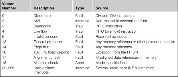
You may have noticed that the fault handler points to the faulting instruction for faults; this is because the handler is likely to rerun the faulting instruction once the underlying reason for the fault is resolved. For example, if a page fault is generated, the operating system will load the page from disk, set up the page table to map the page, and then rerun the instruction. Instructions that generate a trap, on the other hand, are not rerun. On other embedded platforms such as ARM, the fault address recorded on the exception is always that of the next instruction to run. However, when all instructions are the same size (32-bits) it’s a trivial matter to establish the faulting instruction; it’s not quite as straightforward with a variable size instruction set. The list of exceptions and interrupts that a processor supports is part of a processor’s architecture definition. All exceptions and interrupts are assigned a vector number. The processor uses the vector assigned to the exception or interrupt as an index into a vector table. On Intel architectures this vector table is called the Interrupt Descriptor Table (IDT). The table provides the entry point to the exception or interrupt handler. IA-32 defines an allowable vector range of 0 to 255. Vectors from 0 to 31 are reserved for architecture-defined exceptions and interrupts. Vectors 32 to 255 are designed as user-defined interrupts. The user-defined vectors are typically allocated to external (to the processor) hardware generated interrupts and software interrupts. Table 5.11 is a partial list of the IA-32 Protected mode exceptions and interrupts. See Chapter 5 of IA-32 Intel Architecture Systems Programming Guide.
Table 5.11. Abbreviated IA-32 Exceptions and Interrupts
In summary, exceptions and interrupts can come from a wide range of sources from the processor core, caches, floating-point units, bus interfaces, and external peripherals. Figure 5.5 shows the wide range of sources.
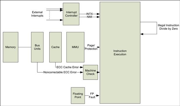
FIGURE 5.5 Exception and Interrupt Sources.
Vector Table Structure
All processors provide mechanisms to translate an interrupt or exception into a handler for the interruption. Different processor architectures provide differing levels of hardware support in identification of the underlying hardware exception. As we mentioned above, external hardware interrupts are assigned a vector. PowerPC and some ARM architectures have a single IRQ line to the processor. The exception handler must then resolve the underlying cause of the interrupt, look up a software-based vector table, and transfer control to the interrupt handler. On Intel processors, the processor hardware itself identifies the underlying cause of the interrupt and transfers control to the exception handler without software intervention. An Intel processor takes a number of steps in the transition to the interrupt handler. Figure 5.6 shows the structures and registers that are used in the process.
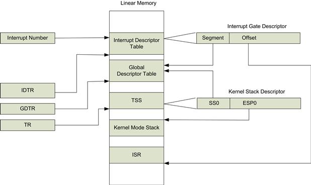
FIGURE 5.6 Interrupt Descriptor Dereferencing.
The IA-32 processor automatically takes several steps in transfer of control to the exception function handler. The hardware interrupt controller sends an interrupt N message to the CPU. The interrupt controller is called the Local Advanced Peripheral Interrupt Controller (Local APIC) on Intel processors. The CPU reads the interrupt descriptor from the interrupt descriptor table (IDT). The interrupt descriptor table is located in system memory. The IDT stores a collection of gate descriptors that provide access to interrupt and exception handlers. The linear address for the base of the IDT is contained in the interrupt descriptor table register (IDTR). The IDT descriptor can contain one of three types of descriptor: task gate, interrupt gate, and trap gate. The IDT contains either an interrupt gate or trap gate descriptor for external interrupts. The difference between an interrupt gate and a trap gate is its effect on the IF flag: using an interrupt gate clears the IF flag, which prevents other interrupts from interfering with the current interrupt handler. The interrupt gate contains the following information:
• Segment selector. The segment selector selects a segment in the global or local descriptor table; this provides a base address for the IRQ handler table.
• Segment offset. This offset is added to the base address found in the referencing of the segment selector to produce the linear address of the ISR handler.
• Privilege level. This is usually set to zero (same privilege level as kernel mode code).
The address of the actual interrupt service routine is
ISR Linear Address =
GDT[(IDTR[Vector Number ].SegmentSelector)].BaseAddress +
IDTR[Vector Number].SegmentOffset
For Linux the values populated in the tables degenerate to the following (the processor still performs the lookups but the value returned is zero):
ISR Linear Address =
IDTR[Vector Number].SegmentOffset
Before the processor transfers control to the ISR, it must identify the appropriate stack to use to save registers. Two situations can occur. The first is when the interrupt privilege is the same level as the currently executing code. This occurs when an interrupt occurs while the processor is running kernel mode software. In this scenario the processor saves the EFLAGS, CS, and EIP registers on the current stack. The other situation occurs when the interrupt privilege level is lower than the currently executing code, for example, when the processor is interrupted while running user mode application code. In this case the segment selector and stack pointer for the stack to be used by the handler are obtained from the Task State Segment (TSS) for the currently executing task. On this new stack, the processor pushes the stack segment selector and stack pointer of the interrupted procedure. The processor then saves the current state of the EFLAGS, CS, and EIP registers on the new stack. The processor then transfers control to the interrupt service routine. The following sections describe the stack frame established by the processor and the resulting software handlers.
Exception Frame
A considerable amount of data must be saved when an exception or interrupt occurs. The state is saved on a stack, and the format of the saved data is known as an exception frame, as shown in Figure 5.7 . The exception frame can be split into two distinct portions: the first is the portion saved automatically by the processor, and the second is the set of additional registers that are saved by operating system interrupt service routine before it loads the software handler that deals with the actual device interrupt.

FIGURE 5.7 Stack Frames.
Some processor-generated exception frames include an error number on the stack. For example, a page fault will provide an error code on the stack frame. These error codes provide additional information such as whether the fault was due to a page not being present or a page-level protection violation.
The actual IRQ function call is usually written in assembly language. The function is then responsible for saving the registers that may be destroyed in the handling of the interrupt. For example, the MACRO SAVE_ALL defined in the Linux kernel file entry_32.s saves all the required registers as part of interrupt handler call. Once the interrupt has been processed, the system must return to normal execution. The IRET instruction will restore the processor to the same state prior to the interrupt (once the software saved state is also unrolled). In a simple embedded system this is the normal mechanism used to return to the pre-interrupt operation; however, in a multitasking operating system environment, the operating system may not necessarily return directly to the task that was interrupted. For example, if the operating system timer IRQ fires while a user process is running, the operating system will save the user space process registers into a process-specific storage area, execute the interrupt handler, and then identify what code should run next. It most likely will execute the kernel scheduler function. The kernel scheduler identifies the process to continue with, and transfers control to that process.
Masking Interrupts
As we discussed, interrupts fall into two classes, maskable and non-maskable interrupts. Processors provide a control mechanism to disable the servicing of interrupts received by the processor core. For Intel CPUs the Interrupt Enable (IF) flag in the EFLAGs register provides the control. If the flag is set, then the processor will service interrupts. If the flag is cleared, the processor will not service maskable interrupts. A number of mechanisms can be used to control the state of the IF flag. First, there is an instruction specifically assigned to allow you to set and clear the flag directly. The STI (set interrupt enable flag) instruction sets the flag, and the CLI (clear interrupt enable flag) clears the flag.
The use of STI/CLI (or its equivalent on other processors) has been quite prevalent in embedded systems to provide a low-cost method of mutual exclusion. For instance, if two threads were working with a linked list, it was quite common to disable interrupts while the pointer updates associated with link element insertion took place. Then the interrupts were re-enabled. This allowed the multiple pointer updates associated with a linked list insertion to be atomic. The mechanism has also been used between interrupt handlers and threads used for deferred processing.
However, two issues arise with this approach. The first issue relates to the introduction of multiple hardware threads in processors (multiple processor cores, or hardware threading on a single core). The STI/CLI instructions mask interrupts on the hardware thread that issued the instruction (the local CPU). Interrupts can be processed by other hardware threads. As a result, the guarantee of atomicity has been lost. In this case other synchronization mechanisms such as locks may be needed to ensure that there are no race conditions. The second issue arises because masking of interrupts can affect the real-time behavior of the platform. Masking interrupt introduces non-determinism associated with the overall interrupt latency performance. In embedded systems, having a deterministic latency time to service specific interrupts can be very important. For both these reasons and others, directly enabling and disabling of interrupts to provide mutual exclusion should be avoided. A case in point: the Linux kernel 2.4 had a significant number of sti/cli calls in the device drivers. The introduction of version 2.6 kernels was aligned with multi-core processors being much more prevalent, and correspondingly there are almost no driver calls left in the drivers for the 2.6.∗ Linux kernel. In fact, function wrappers for sti()/cli() have been removed from the kernel.
The interrupt flags can also be affected by the following operations: the PUSHF instruction saves the flags register onto the stack where it can be examined, and the POPF and IRET instructions load the flags register from the stack, and as a result can be used to modify the interrupt enable flag.
The interrupts are automatically masked when you enter an interrupt handler, and the driver or operating system will re-enable interrupts.
Acknowledging Interrupts
When a device indicates an interrupt request to the interrupt controller, the interrupt controller typically latches the request in an interrupt status pending register. The interrupt handling software must eventually clear the interrupt in the device and also indicate to the interrupt controller that the interrupt has been serviced. The device driver is typically responsible to consume all events that are associated with the interrupt and explicitly clear the source on the device. The interrupt controller (such as 8259/IOAPIC) must also be notified that an interrupt has been processed so the interrupt controller state can be updated.
The device interrupts on Intel systems may be presented to the interrupt controller as either edge- or level-triggered interrupts. For level-based interrupts, the device will de-assert the interrupt line once the underlying device event has been acknowledged. Level-triggered interrupts consist of a message sent to the interrupt controller that an interrupt has been raised. The actual interrupt line is now represented by a message being routed on a bus. There is no message signal to indicate that the interrupt has been cleared. The legacy (8259) interrupt controller has a register known as the End of Interrupt (EOI) register. The system interrupt handler may have to write to this register depending on the configuration.
Interrupt Latency
It is important to understand both the latency and the jitter associated with interrupt latency on embedded systems, as shown in Figure 5.8. The interrupt latency is defined as the time from when the hardware event occurred to the time when the software handler starts to execute. The contributions to the overall latency (and its variability) are:
• Hardware detection of the interrupt and its propagation to the processor core.
• Waiting for the interrupt to be at the appropriate level, for example, waiting for a current interrupt handler to complete.
• Recognition by the processor either by waiting for the current instruction to complete or by interrupting the current instruction at the next available cycle.
• The processor must identify the linear address of the interrupt handler. On Intel processors this requires reading the GDT and IDT tables, which could result in cache and translation look-aside buffer misses.
• The processor saves critical registers and transfers control to the interrupt handler.
• The interrupt handler then saves the remaining registers before the tradition C interrupt handler is called.
As you can see, quite a few steps are involved between the interrupt event and the actual transfer of control to the handler. In most operating systems the first handler must do very little work directly. Typically, the interrupt is just acknowledged and a signal to another thread or context is generated. The rest of the interrupt processing then takes place in the signaled task. This latency before this next task executes is generally larger than the original latency between events and interrupt handler. At a platform level, additional latencies such as system management interrupts, power-saving sleep states, and CPU frequency throttling can all affect the jitter of the interrupt response.
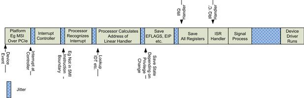
FIGURE 5.8 Components of Interrupt Latency.
As soon as you start to discuss interrupt latencies in a system, the question of real-time behavior arises. Is your system hard real time or soft real time, for instance? It depends on your target application and the expected deadlines imposed by the application and how it interacts with the interrupt events. For real-time platforms, the actual delay between interrupt and service routine, consistency of time delay, and a maximum upper bound are all important criteria. As you can see in Figure 5.8, there can be a number of delays before the interrupt is called. The nominal interrupt latency delay for between the raising of an interrupt to the execution of the handler is on the order of microseconds.
Memory Mapping and Protection
For the most trivial of embedded processors, the address space that the processor runs in is the same as the physical addresses used in the system. That is, the pointers used by your program are used directly to decode the physical memory, peripherals, and external devices. These systems are known as Memory Management Unit (MMU)-less processors, to which category the ARM M3 and older ARM7 TDMI belong. All programs and processes live in the same overall address space. The executable running on such a device is typically a monolithic image (all linked together). Most of the system runs either a single program or an RTOS. It is unusual to run a general-purpose operating system such as Linux, although a limited version of Linux is available for such devices, known as uCLinux.
In MMU-less devices, there is often the need to provide some form of protection between different aspects of the system. This level of protection is provided by the provisions of a memory protection unit (MPU). The MPU defines the portions of the system memory map that are valid and provides different access control for system and user processes. On some SOC devices the MPU also controls whether a memory region is cacheable. The MPU typically supports a limited number of defined regions.
Given the increasing complexity of the software running on embedded systems, it is increasingly likely that the SOC has a significantly more capable protection mechanism known as a memory management unit (MMU). The MMU provides protection and a fine-grained address translation capability between the processor’s address space and the physical addresses used throughout the system. The processor address space is known as the linear address space on Intel processors and is often referred to as virtual address space by other architectures. The MMU has support for different translations based on the currently active process. This allows each process to live in the same linear address space, but actually be resident in different physical address spaces. The MMU is also a fundamental building block that allows a processor to support a virtual memory system. A virtual memory system allows the operating system to overcommit the amount of memory provided to applications by having a mechanism to move data in and out from a backing store typically on a disk. This mechanism is known as paging.
Embedded systems do not typically employ the use of virtual memory paging. For a number of reasons, embedded systems shy away from the use of virtual memory paging: paging can introduce significant non-determinism to the behavior of the system, and page faults can take a significant number of processor cycles to handle. A page fault requires copying the processes’ virtual memory page from a disk to an allocated physical memory page, an operation that is tens of thousands of times slower than accessing memory. If a process triggers a page fault, it is suspended until the page fault handler completes the data move. While embedded systems do require nonvolatile storage, it is unlikely that a traditional spinning hard disk medium is used due to environments, cost, serviceability, and power considerations. Flash memory is the predominant nonvolatile storage mechanism used in embedded systems, and a paged virtual memory system would generate a significant number of transactions to the flash-based file system. Given that flash-based nonvolatile storage lifetime is measured in terms of erase cycles, paging could adversely affect the product’s longevity. Most real-time operating systems do not actually support paging for the reasons mentioned above. The Linux operating system does support paging (also known as swapping) by default. It can be disabled at kernel build time by setting the CONFIG_SWAP=N. Swapping can also be disabled at runtime using the root command swapoff -a, but the swap partition or file will remain and consume storage resources.
PROTECTION ON INTEL ARCHITECTURE
The IA-32 architecture has been one of the most consistent and pervasive architectures to date. The earliest products in the architecture (8086 and 80286) provided memory protection by way of segmentation. Given that Intel architecture has always been backward compatible, the segmentation features remain. However, most operating systems use the MMU capabilities for protection (as well as address translation).
Memory Management Unit
The memory management unit logically sits between the processor internal bus and the memory hierarchy—the first level of the hierarchy is most likely the processor’s first level cache on modern embedded processors. The MMU provides the following key features:
• Address translation. The MMU provides per process address translation of linear (virtual) address to physical addresses.
• Protection. The MMU entries provide privilege checking and read/write protection of memory. Privilege checking ensures that the processor has the correct privilege level to access a particular memory region.
• Cache control. Different memory regions requires different cacheability attributes.
When using the MMU, the memory map is divided into pages (typically 4 kB each). The operating system maintains a page directory and a set of page tables to keep track of the pages. When a program (or task) attempts to access an address location in the linear address space, the processor uses the page directory and page tables to translate the linear address into a physical address and then performs the requested operation (read or write) to the memory location, as illustrated in Figure 5.9.
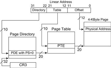
FIGURE 5.9 Liner Address Translation.
The design of the MMU translation structure must optimize for lookup efficiency and overall table size. To meet these goals, both table-based lookups and hashed data structures are used in processors today. On IA-32 architectures the MMU use a page table structure to look up a page descriptor associated with a virtual address. In a 32-bit system, with a page covering 4 kB of physical memory, the MMU table would require 1,048,576 contiguous entries to cover entire 4 GB addressing if the table were constructed as a simple lookup table using high-order address bits of the linear address. Processes generally only use a small fraction of the available 4 GB virtual address space. In addition, the page table structures are replicated once for the kernel and for each process in the system. So using a simple lookup table for paging would be very costly in memory usage. IA implements the paging tables as a sparse data structure with a page table hierarchy consisting of two levels of indirection.
The base physical address of the page directory value is specified in the control register CR3[31:12]. The lower 12 bits of the address are zero, which means the page directory must be aligned on a 4-kB boundary. The CR3 register also contains some cacheability information for the directory itself.
A page directory comprises 1024 32-bit entries. The Page Directory Entry (PDE) is selected using the high-order address bits (31-22) from the linear address along with a base address provided by CR3. The page directory entry contains the two following fields—a page present indicator and the base address of a page table that is the next level of the sparse table hierarchy (if the PDE contains an entry for 4-kB pages).
When the page present bit is set, it indicates that the base address is valid. The page directory entries are created and managed by the operating system. Table 5.12 shows the bit definitions for the directory descriptor entry.
Table 5.12. Directory Descriptor Entry
| Descriptor Bit | Bit Name | Description |
| bit 0 | Present | 1 if the page descriptor is present and valid |
| bit 2 | R/W | Read/write; if 0, writes may not be allowed to the 4-MB region controlled by this entry |
| bit 2 | U/S | User/supervisor; if 0, accesses with CPL = 3 are not allowed to the 4-MB region controlled by this entry |
| bit 3 | PWT | Page-level write-through; indirectly determines the memory type used to access the page table referenced by this entry |
| bit 4 | PCD | Page-level cache disable; indirectly determines the memory type used to access the page table referenced by this entry |
| bit 5 | A | Accessed; indicates whether this entry has been used for linear-address translation |
| bit 6 | D | Ignored |
| bit 7 | PS | If CR4.PSE = 1, must be 0 |
| bits 8–11 | Ignored | Should be zero |
| bits 12–31 | Addr | Physical address of 4-kB aligned page table referenced by this entry |
If a memory access is generated to a memory region without a valid page descriptor (including “non-present”), the MMU generates a page fault exception. The page fault is a precise exception and the instruction pointer of the memory access can be identified in the exception handler. When using an RTOS, this is often a result of not defining the memory map correctly or general program errors.
The next level in the hierarchy are the page tables. If the page directory entry contained a valid page table entry, then the MMU looks up the page table entry by means of a page table lookup using bits 12 to 21 from the linear address. Table 5.13 shows a page table entry for a 32-bit system.
Table 5.13. Page Table Entry (That Maps a 4-kB Range)
| Page Descriptor Bit | Bit Name | Description |
| bit 0 | Present | 1 if the page descriptor is present and valid |
| bit 2 | R/W | Read/write; if 0, writes may not be allowed to the 4-kB region controlled by this entry |
| bit 2 | U/S | User/supervisor; if 0, accesses with CPL = 3 are not allowed to the 4-kB region controlled by this entry |
| bit 3 | PWT | Page-level write-through; indirectly determines the memory type used to access the 4-kB page referenced by this entry |
| bit 4 | PCD | Page-level cache disable; indirectly determines the memory type used to access the 4-kB page referenced by this entry |
| bit 5 | A | Accessed; indicates whether software has accessed the 4-kB page referenced by this entry |
| bit 6 | D | Dirty; indicates whether software has written to the 4-kB page referenced by this entry |
| bit 7 | PAT | If the PAT is supported, indirectly determines the memory type used to access the 4-kB page referenced by this entry |
| bit 8 | Global | Global; if CR4.PGE = 1, determines whether the translation is global |
| bit 9-11 | Ignored | Should be zero |
| bit 12-31 | Address | Physical address of 4-kB aligned page referenced by this entry |
The key field in the page table entry is the physical address of the 4-kB page being looked up; this address provide bits 31:12 of the actual physical address, while the remaining bits 11:0 are provided by bits 11:0 from the virtual address, which are used as an offset into the 4-kB physically addressed page.
This is a summary of the address translation for valid entries using 4-kB pages.
Directory Base Physical Address = (CR3 & ~0xFFF)
Page Table Base = Directory Base Physical Address[Linear Address[31:22]].Addr
4KPageBase = Page Table Base[Linear Address[21:12]].Addr
Physical Address = 4KPageBase + Linear Address[11:0]
The section above concentrated on the translation function provided by the MMU, but the descriptor and page table entries provides a number of other data elements that warrant further discussion:
• Write protection. The MMU will generate a general-protection fault if an attempt is made to a write to a protected page. The operating system would normally treat this as a program fault. Write-protected pages are also used to implement “copy on write” strategies in an operating system. For example, when a process forks in Linux, the forked process is logically a full copy of the forking process along with all its associated data. At the start of the forked process all of the data are identical to the process that carried out a fork, so instead of a new physical pages for the forked process, each physical page in the process is marked as write protect and mapped to each copy of the forked processes. When any of the processes actually updates a page, the write protection fault triggers the operating system to actually make a copy of the page for the process that triggered the fault. This effectively maximizes the number of identical shared virtual pages mapping to the same physical page and only allocates memory for pages that are different between the forked processes. This technique is known as “copy on write” (COW).
• Privilege. The MMU can allow the kernel process to have full visibility of and access to the user space pages, while preventing user space programs from accessing kernel structure (unless mapped to the user space program). Specifically, if the U/S (User/Supervisor) bit in the page table is zero, then user space (CPL = 3) processes cannot access the memory covered by this page.
• Accessed. The MMU updates the accessed bits within the page descriptor if the processor has accessed a memory location in the page. The accessed bit in the page descriptor can be used to identify the “age” of a page table entry. The operating system swap process periodically resets the accessed bits in the page tables. Then when a process accesses a page, the processor can identify which pages have been used since the values were last reset. On Linux this forms the basis of a least recently used (LRU) algorithm that selects the candidate pages that may be swapped to mass storage.
• Dirty. The MMU updates the dirty bit of a page if it has been written to any address in this page since the bit was last cleared. This is used with the operating system’s paging/swapping algorithm. When a page is first swapped in from disk to memory, the dirty bit is cleared by the operating system. If a process writes to this page subsequently, the dirty bit is set. When the time comes to swap out the page, the dirty bit is tested. If the page is dirty, which means one or more locations in the page are updated, then the page must be written back out to disk. If, however, the dirty bit is zero, then the page does not have to be written out to the disk because the backing store is still valid.
• Memory cache control. On Intel architectures, the control of the caches and memory ordering is a complex area. The page tables contribute page-granular control of this cacheability and memory ordering behavior. The cacheability can also be defined by Memory Type Range Registers; when a conflict arises the most conservative configuration will be selected. For example, if the page table indicates that the area is cached but an MTRR indicates un-cached, un-cached is the safest, most conservative option. The processor caches are described later in this chapter.
• Global pages. These are pages that are usually active for operating system contexts (kernel and all processes). It facilitates optimization in translation cache behavior, as described in the following section.
The MMU can also prevent execution from data pages, but this feature is only available in PAE or 64-bit mode.
The Intel architecture supports three different modes for the MMU paging, namely, 32-bit, Physical Address Extension (allows a 32-bit CPU to access more than 4 GB of memory), and 64-bit modes. In the context of embedded platforms we will focus on the 32-bit configuration. The nominal page size is 4 kB; 2-MB and 4-MB (often called large page) pages are supported depending on the mode.
Translation Caching
As you may predict, the translation from a virtual address to a physical address would be a very costly event if it were required for every single memory transaction. For the Intel architecture each translation could result in two dependent reads. To reduce the impact of translation, processors generally employ techniques to cache the translation and additional details it provides in a translation cache. This is usually very effective given that page table access exhibits excellent temporal locality. These are generally known as translation look-aside buffers (TLBs). The TLB is typically constructed as a fully or highly associative cache, where the virtual address is compared against all cache entries. If the TLB hits, the contents of the TLB are used for the translation, access permissions, and so on. The management of the TLB is shared between the operating system and hardware. The TLB will allocate space automatically for new entries, typically by employing a (Least Recently Used) LRU policy for replacement. There is no hardware coherency enforcement between the TLBs and the page tables in memory. If software modifies a page or table entry (e.g., for resetting Accessed bit or changing the mapping) directly, then the TLBs must be invalidated. Otherwise, there is a risk that an out-of-date translation is used. The INVLPG instruction invalidates a single TLB entry; software writes to the CR3 register can be used to invalidate the entire TLB. On some processors, the TLB is managed in software with hardware-assist functions to perform the page walks.
An optimization can improve the effectiveness of the TLB during process context switches (kernel/user and user/user). The page tables provide a Global bit in the page entries. If this is set, then the page table entry is not flushed on a global TLB flush event.
The current Intel Atom processor has a number of separate TLB structures:
• Instruction for 4-kB page: 32 entries, fully associative.
• Instruction for large pages: 8 entries, four-way set associative.
• Data 4-kB pages: 16-entry-per-thread micro-TLB, fully associative; 64-entry DTLB, four-way set associative; 16-entry page directory entry cache, fully associative.
As an embedded software developer, you may find yourself tuning the overall platform execution. High TLB miss rates can contribute to poor overall system performance. It is prudent to review performance counters in the platform and focus on the overall TLB miss rate. There are a few strategies to reduce the overall system TLB miss rate. The first is to consolidate program and data hot spots into a minimum memory footprint, which reduces the number of pages and subsequently TLB entries needed during the hot spot execution of the platform software. This can be achieved by linking the hot spot objects close together. An additional technique to consider is using large pages to cover hot spot areas. The ability to use pages other than the standard 4 kB is dependent on the operating system providing such control. A Linux kernel feature known as HughTLB provides a memory allocation mechanism that allocates a contiguous piece of physical memory that is covered by a single large TLB entry. If you have an application that jumps around (a nontechnical term for exhibits poor locality) a large data structure, using a large page entry could significantly reduce the TLB misses.
MMU and Processes
Thus far, all the discussion on the memory management unit has been relatively static and to a single set of translation tables. Each time the operating system makes a transition between processes (between user and kernel, or between user and user space process) the active page tables must be changed. The transition between processes is known as a context switch. For example, each user space program “lives” in the same virtual address space, which maps to the process-specific physical RAM pages; therefore, we need to apply a different translation from virtual to physical pages when the new process executes.
A processor can use a number of mechanisms to incorporate the processes’ specific information in the address translation. On some architecture, the translation tables contain process identification information within the table; on Intel architectures the MMU uses the contents of CR3 as the base pointer to the active page table. The operating system updates the CR3 register each time the operating system changes process space. When the CR3 register is written to, any cached translations in the TLB are for the most case invalid, the act of writing to the CR3 register invalidates ... all but nonglobal TLB entries. The global entries are entries that are guaranteed to be consistent for all processes (by operating system convention).
Although it is becoming less common due to robustness and security concerns, embedded systems often set up very simple memory maps where processes live in the same linear address space. In this case the vast majority of TLBs may be made global to reduce the cost of flushing the TLBs; however, processes can subsequently see other processes’ memory.
On ARMv4™ and ARMv5™ (such as Intel XScale) processors, the cache is virtually indexed and virtually tagged. The index and tag fields are both derived from the virtual address. This means that the cache can be looked up without looking up the TLB. The TLB translation search can happen in parallel to the cache lookup. The downside of this approach is that the cache is generally invalidated on a context switch. On ARMv6™ and ARMv7™ processors caches may be virtually indexed and physically tagged. This reduces the number of cached invalidates, but the cached lookup mostly occurs after the virtual to physical address translation occurs. To support multi-processor or hardware coherency, the caches are physically indexed and tagged (as is the case for Intel architecture).
Memory Hierarchy
Providing a higher-performance memory subsystem is critical in maximizing the performance of the CPU. If the memory subsystem does not complete transactions quickly enough, the processor eventually stalls. There are many microarchitecture techniques that strive to keep the processor doing useful work while memory transactions are in flight, but it is impossible to always keep the processor busy at all times. When the processor is waiting for the memory subsystem, the processor stalls and is no longer doing useful work. These stalled cycles have a direct impact on the effective clocks per instruction (often called CPI) taken by your application; that is, stalls directly impact the performance of the system.
The processor may stall on both read and write operations. Stalling on reads is relatively intuitive; the program cannot make forward progress until the memory read provides the required value in the register in order for the program to progress. Stalls caused by memory writes are less likely but can still occur. The processor may stall on writes when the processor generates memory write transactions at a rate that is higher than the ability of the memory subsystem to consume the memory writes. The microarchitecture of the processor will typically have several stages of write buffering to ensure that the processor does not stall. This write buffering also serves to allow the memory subsystem to prioritize memory reads over writes. In general, the memory subsystem always prioritizes reads over writes until write transactions build up to such an extent that the processor stalls on writes. You may have noted that the prioritization of reads over writes in the memory subsystem causes reordering of the memory transactions. Naturally, reordering transactions without any regard to the program order of the memory transactions would have a catastrophic effect on program execution. To resolve this, key program order guarantees are maintained. For example, if a read follows a write to a memory address and the write command is still in a write buffer, the write buffer must be snooped and provide the value for the read. We discuss ordering of transactions and how they interact with the I/O subsystem later in the chapter.
We have briefly touched on the effects of not matching the memory system performance to that of the CPU. The strategies for maximizing the performance of the memory subsystem come from the optimization of subsystem design and economics. The ideal device would provide large amounts of the extremely fast memory technology tightly coupled to the processor core. Unfortunately, the highest density and fastest memory technology typically has the highest cost associated with it. The following are different types of memory, as illustrated in Figure 5.10:
• Logic gate memory. This is typically used for intermediate buffering, such as write buffers.
• Static RAM (SRAM). SRAM cells are used on devices for caches and small amounts of RAM that is close to the processor. Access time for SRAM/caches would be in the order of 1–2 CPU core clocks. The caches are also broken down into separate levels (such as Level 1 and Level 2) with increases in access latency and increasing density as the levels increase.
• Dynamic RAM (DRAM). DRAM technology provides the bulk of the memory requirements for embedded systems. Typically access cycles are 100ns. The technology required to create high-density DRAM devices is not the same as the silicon process technology required for high-speed logic or SRAMs. As a result, DRAM memory is usually external to the SOC. In some limited cases, the DRAM is placed in the same package as the processor/SOC, but at the time of writing it is a costly operation and not common.
• Mass storage. When mass storage is used as part of the paging virtual memory system. Access to mass storage even for SSD-based media requires thousands of CPU cycles.
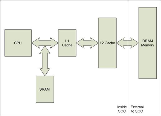
FIGURE 5.10 Memory Hierarchy.
Local Memory
On some embedded SOC devices dedicated SRAM is provided on die. The SRAM device is mapped to a unique address in the memory map and must be explicitly managed by the application or operating system. This is usually achieved by using a specific tool chain linker section and mapping specific data structures with your application to this tool chain linker section. The access times are usually similar to that of an L1 cache (perhaps a little faster because there are no tag lookups required). The contents that you place in these RAM devices are really a function of the application; they are often used to increase the determinism of interrupt handing software because access to the memory cannot miss, as is the case for caches. These embedded SOC SRAMs are not usually coherent with the remainder of the I/O system. This local memory is sometimes called tightly coupled memory (TCM).
Cache Hierarchy
The fastest memory closest to the processor is typically structured as caches. A cache is a memory structure that stores a copy of the data that appear in main memory (or the next level in the hierarchy). The copy in the cache may at times be different from the copy in main memory. When a memory transaction is generated by the processor (reads/writes), the cache is searched to see if it contains the data for the requested address. The address used in the cache structure may be a virtual or physical address depending on whether the cache is situated before the MMU translation or after. For example, the level one cache of the Intel XScale processor is addressed using virtual addresses. Caches in the Intel Architecture processors are all addressed with physical addresses. The term tag is used to refer to the fields within the address that are used to search the cache for a match.
Caches are structures that take advantage of a program’s temporal and spatial locality:
• Temporal locality. If a memory location was accessed then it is likely to be accessed again soon (in time).
• Spatial locality. A program is likely to access a memory address close by shortly after the current access.
The caches themselves are often organized in a hierarchy, again with increasing access times and increased size. Even though the technology of the SRAMs is usually similar for L1 and L2 caches, the L2 cache takes longer to return the contents of a hit as it is farther from the core, and it takes longer to search a larger cache. The L1 cache is usually close to the same frequency as the core, whereas the L2 is often clocked at a slower speed.
Theoretically, cache structures can be organized in many different forms. Two extreme implementations are the following:
• Direct mapped. The tag is used to perform a direct lookup in the cache structure. The contents of the cache for the virtual address can reside in exactly one location within the cache.
• Fully associative. The tag is used to search the cache for a match; however, any cache location may contain the entry. Unlike the direct mapped implementation where no comparisons must be made, every entry in the fully associative cache must be compared with the tag. Comparing the tag with all entries requires complex combinational logic whose complexity grows the larger the cache size. This is sometimes known as content addressable memory.
In reality, neither approach is feasible; the cache structures are a hybrid of both the direct mapped and fully associative. The structures created on Intel processors are N-way set associative, where N is a different number based on the product and level of the cache. The (physical) address used to look up a set associative cache is divided into three separate fields:
• Tag. The tag field within the address is used to look up a fully associative set. The set consists of N ways, which all must be matched against the tag. The tag field is usually composed of the upper address bits within the physical address.
• Set index. The cache is split into M sets, and this index is used to directly select the set, which is then searched with the tag.
• Offset/displacement. Each cache entry is called a line. The offset selects the actual word within the cache line to return.
Figure 5.11 shows the logical structure of a 24-K Intel Atom instruction cache.

FIGURE 5.11 Six-Way Set Associative 24-K Data Cache.
As a software designer, the cache structure can be largely transparent; however, an awareness of the structure can help greatly when you start to optimize the code for performance. At a minimum, be aware of the cache line size and structure your data such that commonly used elements fall within the same cache line. The Intel Atom platform has the following caches, all with a cache line size of 64 bytes:
• 32-K eight-way set associative L1 instruction cache.
• 24-K six-way set associative L1 data cache.
• 512-K eight-way set associative unified instruction and data L2 cache.
Allocation Policy
The cache allocation policy dictates whether the cache should allocate space based on the transaction type from the processor. Two primary modes of operations are supported by embedded processors. The first is read-only allocate; this occurs when the processor performs a memory read that misses the cache. The cache will identify which line to evict from the cache, usually based on a least recently used (LRU) algorithm. This process identifies which way to evict from the set. The data will be fetched from the next level memory hierarchy and both placed in the cache and returned to the processor. In addition to allocation on read, some embedded processors also support allocation on a write transaction. In this case a similar set of events occurs; a line must be evicted, the contents of the associated cache line are populated from the next level of the memory hierarchy, and then the processor write data are merged into the cache line in the cache. There is an additional policy that dictates whether the data will also be written to memory (as well as the cache) immediately; this is known as write-through. The normal cache mode for the Intel Atom processor is write allocate.
When a cache miss occurs, the full cache line must be brought into the cache. This requires a cached line memory read to occur. This transaction generally appears as a burst read to the memory. The normal operation is for the memory controller to return the words in ascending memory order starting at the start of the cache line. Some platforms support a feature known as Critical Word First (CWF). In this mode, the memory controller first returns the actual requested contents of the memory location that missed the cache (the word), followed by the remainder of the cache line. The CWF feature reduces the latency to the processor for the missed transaction.
The Intel platforms generally have larger cache structures than competing products in the same segment. Larger caches have a lower miss rate, and as result the SOCs based on the Intel Atom do not provide this feature.
Exclusivity
If there are multiple levels of cache in a system, the question arises, can any entry reside in a number of levels of the cache at the same time? Inclusive cache hierarchies ensure that data that is in a level one cache will have a copy in the level two cache, whereas non-inclusive caches will guarantee that data will be resident in only one level at any time. SOCs based on the Intel Atom make no such guarantees and are neither exclusive nor inclusive, although the likelihood is that data in the level one cache would usually also reside in the level two cache.
Whether the caches L1, L2 (and Last Level Cache) are mutually exclusive, mutually inclusive, or a mixture of both depends on the micro architecture of the processor and is not usually architecturally defined. In any respect, the hardware will ensure cache consistency and the correct program behavior.
Memory Types
Different regions of system memory on a platform require different attributes when the memory system interacts with them. For example, portions of the memory map that contain peripheral devices (within or outside the SOC) must not be marked as a cache region. Similarly, general-purpose memory for the operating system, applications, and such is mapped as cacheable. Most systems often provide a register-based mechanism to provide course grained memory attributes. The register typically consists of a base address, range of the register, and the attributes to set for access to memory covered by the register. In the Intel processors, the Memory Type Range Registers (MTRRs), which are machine specific, are provided. In more advanced cases the memory management page tables, as described in the previous section, are used in addition to the MTRRs to provide per page attributes of a particular memory region. Processors such as the Intel XScale enable application memory type classification using the MMU page tables.
On Intel architectures, there are five types of classification that can be assigned to a particular memory region:
• Strong Un-cacheable (UC). System memory locations are not cached. All reads and writes appear on the system bus and are executed in program order without reordering. No speculative memory accesses, page-table walks, or prefetches of speculated branch targets are made. This type of cache control is useful for memory-mapped I/O devices. When used with normal RAM, it greatly reduces processor performance.
• Un-cacheable (UC-). Has the same characteristics as the strong un-cacheable (UC) memory type, except that this memory type can be overridden by programming the MTRRs for the write combining memory type.
• Write Combining (WC). System memory locations are not cached (as with un-cacheable memory) and coherency is not enforced by the processor’s bus coherency protocol. Speculative reads are allowed. Writes may be delayed and combined in the write combining buffer (WC buffer) to reduce memory accesses. If the WC buffer is partially filled, the writes may be delayed until the next occurrence of a serializing event, such as a serializing instruction such as SFENCE, MFENCE, or CPUID execution, interrupts, and processor internal events.
• Write-Through (WT). Writes and reads to and from system memory are cached. Reads come from cache lines on cache hits; read misses cause cache fills. Speculative reads are allowed. All writes are written to a cache line (when possible) and through to system memory. When writing through to memory, invalid cache lines are never filled, and valid cache lines are either filled or invalidated. Write combining is allowed. This type of cache control is appropriate for frame buffers or when there are devices on the system bus that access system memory but do not perform snooping of memory accesses. It enforces coherency between caches in the processors and system memory.
• Write-Back (WB). Writes and reads to and from system memory are cached. Reads are fulfilled by cache lines on cache hits; read misses cause cache fills. Speculative reads are allowed. Write misses also cause cache line fills, and writes are performed entirely in the cache. When possible write combining is allowed. The write-back memory type reduces bus traffic by eliminating many unnecessary writes to system memory. Writes to a cache line are not immediately forwarded to system memory; instead, they are accumulated in the cache. The modified cache lines are written to system memory later, when a write-back operation is performed. Write-back operations are triggered when cache lines need to be reallocated, such as when a new cache line must be allocated when the cache is already fully allocated (most of the time). This type of cache control provides the best performance, but it requires that all devices that access system memory on the system bus be able to snoop memory accesses to ensure system memory and cache coherency. This is the case for all systems based on Intel architecture.
• Write Protected (WP). Reads come from cache lines when possible, and read misses cause cache fills. Writes are propagated to the system bus and cause corresponding cache lines on all processors on the bus to be invalidated. Speculative reads are allowed.
The majority of embedded systems provide simple cache/not-cached memory type attributes. At first look, the Intel architecture capabilities appear overly complex, but the fine-grained approach affords selection of optimal behavior for any memory region in the system with the effect of maximizing the performance.
For a 2.6.34 kernel running on an Intel Atom platform with 1 GB of memory, the following Linux command shows the MTRR settings.
ubuntu-atom1:/proc$ cat /proc/mtrr
reg00: base=0x00000000 ( 0MB), size=1024MB: write-back, count=1
reg01: base=0x3f700000 (1015MB), size= 1MB: uncachable, count=1
reg02: base=0x3f800000 (1016MB), size= 8MB: uncachable, count=1
The first region sets the DRAM as write-back cacheable, the typical setting. The Linux /var/log/Xorg.0.log file indicates that the graphics frame buffer is at 0x3f800000.
(EE) PSB(0): screnIndex is:0;fbPhys is:0x3f800000; fbsize is:0x007bf000
(--) PSB(0): Mapped graphics aperture at physical address 0x3f800000
Linux has set up the third MTRR (reg02) to provide the attributes for graphics aperture. However, the page tables have set up the region as write-combining, overriding the MTRR UC- setting.
Cache Coherency
A number of agents other than the processor access system memory. For example, a peripheral such as a network interface must read and write system memory through direct memory access to transmit and receive packets. When the processor generates a network packet to be transmitted on the network, the system must ensure that the DMA engines of the network interface get the most recent consistent data when it reads system memory for the packet. Conversely, when a processor reads data written by the network card, it should get the most recent content from the memory. The mechanism that manages the data consistency is known as cache coherency.
To ensure that the contents read by the DMA engine are correct, there are two approaches. The first is to ensure that the system memory contents reflect the latest payload before the NIC issues the DMA read. The NIC driver could use software instruction to flush all cache lines associated with packet. This is a costly operation, but not untypical on some embedded SOC platforms. The second approach calls for dedicated logic to search the cache when other agents are reading and writing to system memory.
Managing coherency using software is the responsibility of each device driver on the platform. The operating system typically provides calls that the driver must call to ensure consistency. For an example of an Ethernet device driver that manages coherence in software, you can review the Linux Coldfire fast Ethernet Driver linux-source-2.6.24/drivers/net/fec.c. The following code segment flushes the dcache lines associated with the packet to ensure memory is consistent before transmission.
flush_dcache_range((unsigned long)skb->data,
(unsigned long)skb->data + skb->len);
On Intel platforms, the hardware maintains coherence by snooping the memory transactions to ensure consistency. The processor maintains cache consistency with the MESI (Modified, Exclusive, Shared, Invalid) protocol. Cache consistency is maintained for I/O agents and other processors (with caches). MESI is used to allow the cache to decide whether a memory entry should be updated or invalidated. Two functions are performed to allow its internal cache to stay consistent:
• Snoop cycles. The processor snoops during memory transactions on the system bus. That is, when another bus master performs a write, the processor snoops the address. If the cache(s) contain(s) the data, the processor will schedule a write-back. The agent performing the read will get the up-to-date values.
• Cache flushing. This is the mechanism by which the processor clears its cache. A cache flush may result from actions in either hardware or software. During a cache flush, the processor writes back all modified (or dirty) data. It then invalidates its cache (that is, makes all cache lines unavailable).
These mechanisms ensure that data read or written to the system memory from an IO agent are always consistent with the caches. The availably of hardware-managed coherence greatly simplifies software development of the operating system device drivers, especially when it comes to debugging—it’s tricky to debug cache coherence issues. Newer ARM Cortex™ A9 processors have introduced a Snoop Control Unit for use with Multicore designs. See http://www.arm.com/products/processors/cortex-a/cortex-a9.php for more details.
You should be aware that even though the system may support cache coherence, it is not sufficient to guarantee that writes issued by the processor can be snooped by the snoop logic. The write may be in a write buffer on the way to the cache or memory subsystem. It may still be important that the driver issues a memory barrier before the hardware is notified that it can read any data. The smp_wmb() in Linux performs this function; if the barrier is not needed on a target system it will degenerate to be a null operation. In the case of PCIe™ devices, device drivers usually perform a read from the device. This is a serialization event in the processor and ensures that all memory writes are visible to any snoop logic.
The Linux kernel has a number of APIs that should be used to manage memory that is coherent with the I/O subsystem. For an example of pci_alloc_consistent() refer to Chapter 8.
MESI
Although largely transparent to the programmer, the cache coherence protocol used is worth a brief mention. In processors that support Symmetric Multi Processing (SMP), the behavior of writes in the system depend on the cache states of other caches in the system, For example, if there is a copy of a memory location in another processor’s cache, then each cache entry associated with the memory location will be in a shared state. When any of the processors write to a cache line in the shared state, the write must be written through to the system bus so that other caches can invalidate their copy (it is no longer valid). The multicore processors use the MESI protocol to ensure that all the caches in the system are coherent and consistent, and ensure that no two valid cache lines can have a different copy of the same address. The MESI protocol’s name comes from the states that each of the cache lines may be in at any point in time: Modified, Exclusive, Shared, and Invalid.
• Modified: The cache line is only present in the current cache and has been modified (is dirty) from the value held in memory. The data must be written back to memory at some point. If another processor attempts to read the data from memory before it has been written back, this cache must “snoop” the read and write back the data as part of a snoop response. If the data has been written back to memory, the state transitions to exclusive.
• Exclusive: The cache line is present in the current cache and is clean, has not been modified, and is the same as the copy in memory. It will be updated to shared if another processor also obtains a copy.
• Shared: Indicates that this cache and others have a copy of the cache line. The cache line is clean and all copies are identical to the copy in memory.
Table 5.14 shows the cache line states and the associated behavior.
Table 5.14. MESI Cache Line States
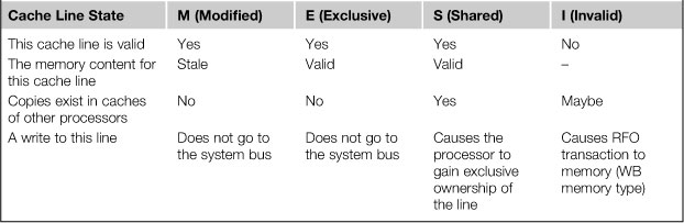
MESI is a very common cache coherence protocol used in multiprocessor designs, including Intel architectures, ARM11™, and ARM Cortex-A9 MPCores.
Bus Addresses
Externally attached devices are typically attached through a bus, usually PCIe or expansion bus interfaces. These external buses most often support direct memory access from the device to system memory. You should note that a device also has a system memory map relative to the bus mastering agent; that is, the memory map as viewed from a device may be different from that as viewed by the processor. When the devices generate addresses for reads or writes, they generate bus addresses, which are then converted to a physical system address at the bus interface point, such as an expansion bus controller or the PCIe root complex. Device drivers use APIs to convert virtual memory addresses to physical system addresses and then to device-relative bus addresses. These bus addresses are populated in the device DMA engines. For traditional 32-bit Intel architecture systems the PCIe bus address maps 1:1 with the physical address used. On most SOCs, however, either there are changes in the size of the address space or translation between bus addresses and system addresses. You should be aware of such translation and abstract the translation when developing your device driver software.
System Bus Interface
In previous generations of embedded systems the processors or system bus was externally exposed on the device, and the system bus was routed throughout the printed circuit board. However, with advances in integration the system bus is now an internal (to the SOC) interconnect. The processor bus within some Intel Atom devices is a derivative of the previously exposed Front Side Bus (FSB). The FSB was the bus that connected the CPU to the Memory Controller Hub (MCH) in older generations of Intel platforms. The memory controller hub feature set is now integrated into the SOC; as a result, the memory controller interface is exposed for direct attachment to the memory devices. On the Intel Atom-based SOC, a bus similar to the FSB logically remains within the SOC.
Memory Technology
At the time of writing the memory technology attached to the processor is usually Double Data Rate Synchronous Dynamic Random Access Memory (DDR3 is common on desktop platforms, while DDR2 is still prevalent on embedded systems). The interface for DDR is defined by the JEDEC organization (reference: http://www.jedec.org). Both the density and bandwidth of the dynamic memory technology have increased considerably over time; however, the latencies associated with memory access have not declined at nearly the same rate. The memory controller and memory devices are highly pipelined. Attributes of the memory hierarchy described above are all structured to try to ensure that the application does not directly experience the latency of a DRAM transaction. To that end, in addition to the cache structure, some platforms have pre-fetchers. A pre-fetcher is a piece of logic that attempts to predict future memory access that will be made based on the history of the application. It then issues a speculative read transaction to the memory controller to bring a likely entry closer to the processor before it is actually needed.
The memory controller can operate in burst and single-transaction mode. Burst mode transactions are significantly more efficient than the single transaction. This burst mode transaction matches well to the cache line fill/write-back behavior of the caches.
More details on the memory interfaces are provided in Chapter 2.
Intel Atom Microarchitecture (Supplemental Material)
The primary view by which a software designer understands a processor-based system is through its architecture definition. From a software viewpoint, the architecture definition is a contract between the platform and the software. The platform behaves in a guaranteed manner in compliance with the architecture definition. The architecture of the CPU in particular changes infrequently over time, and there are relatively few of them in existence. For example, in the embedded processor space the primary architectures are IA-32, ARM, MIPS™, and PowerPC. The architecture itself can evolve by adding capabilities; each architecture has differing approaches to the growth and management of the architecture over time. The IA-32 architecture takes one of the most rigorous approaches to ensure that software written for any previous microarchitecture continues to run on the latest microarchitecture. Other architectures such as ARM have chosen to allow for forward compatibility only. For example, the ARM Cortex M3 runs a subset of the ARM ISA known as Thumb2, so code compiled for an ARM Cortex M3 will run on an ARM Cortex A9 but not vice versa. Each approach brings about its own trade-offs in silicon complexity and reuse of software.
The microarchitecture of a product is not part of the architectural contract with the software. It is a specific implementation that complies with the architecture. The microarchitecture of a product changes more frequently than the architecture and represents a specific implementation that is tuned to fulfill specific optimizations such as core speed, power, or both. The IA-32 architecture includes Intel486®, Pentium® processors, Intel Core, Core 2, and Intel Atom microarchitecture. The microarchitecture defines attributes of the implementation such as in-order/out-of-order instruction processing, the depth of the instruction pipeline, and branch prediction. In particular, the software designer should be aware of the microarchitecture of the CPU when tuning the system to maximize its performance or power for the target architecture. The architecture definition will guarantee that your software will always execute. Awareness of the microarchitecture (especially in the compiler) will help ensure that the code runs optimally. To ensure optimal execution on all platforms, the Intel Performance Primitive have a code path for all supported microarchitectures, each specially tuned. A CPU dispatch block establishes the best code path to execute depending on the CPU identifier.
Microarchitecture
The Intel Atom processor microarchitecture consists of the set of components on the processor that enables it to implement and provide support for the IA-32 and Intel 64 ISA. Embedded software developers need a basic understanding of the microarchitecture if they are engaged in low-level assembly language programming, such as developers working on device drivers or performance-critical portions of an application. Embedded software developers focused on utmost performance must also understand the microarchitecture and its implications for high-performing assembly or machine language. The ability to inspect assembly language code or a disassembly of an application and to understand the difference between high-performing and low-performing code sequences when executing on the Intel Atom processor is critical for product success. This section provides the basic understanding of the microarchitecture required to do so.
Figure 5.12 is a high-level depiction of the Intel Atom processor microarchitecture. At a first level, the microarchitecture of the initial Intel Atom processor is classified as an in-order, superscalar pipeline. The term in-order means that the machine instructions execute in the same order that they appear in the application. The term superscalar means that more than one instruction can execute at the same time. The Intel Atom processor is classified as two-wide superscalar since it has the ability to execute and retire two instructions in the same clock cycle. Modern processors are pipelined, which allows multiple instructions to be in different stages of processing at the same time.

FIGURE 5.12 Intel Atom Processor Microarchitecture.
The integer pipeline for the Intel Atom processor is detailed in Figure 5.13. The pipeline is divided into six phases of instruction processing:
The integer pipeline consists of 16 stages and the floating-point pipeline consists of 19 stages. In normal pipeline operation each stage takes one cycle to execute. The number of stages for each phase is detailed in Table 5.15. Note that each phase is pipelined; for example, it is possible for three instructions to be in the different stages of the instruction fetch phase (IF1, IF2, and IF3) at the same time.
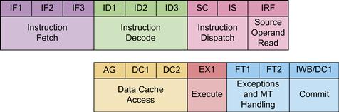
FIGURE 5.13 Integer Pipeline.
Table 5.15. Intel Atom Processor Pipeline
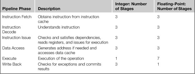
For the integer pipeline, the instruction fetch phase is three stages and the instruction decode is three stages. Instruction issue consists of three stages and data access consists of three stages. Instruction execution consists of one stage and write back consists of three stages. For floating-point instructions, the instruction fetch consists of three stages and instruction decode consists of three stages. Instruction issue consists of three stages and data access consists of three stages. Instruction execution consists of seven stages and write back consists of one stage. There are many exceptions when an instruction can take longer to execute than 16 or 19 cycles; examples include division operations and instructions that decode in the microcode sequencer.
As mentioned previously, the Intel Atom processor microarchitecture is in-order. You can understand what in-order means by comparing it to an out-of-order microarchitecture such as the Intel Core i7 processor. Consider the sequence of instructions listed in Figure 5.14, which has the following program-specified dependencies:
• Instruction 2 is dependent on the result of instruction 1.
• Instruction 3 is dependent on the result of instructions 2 and 1.
• Instruction 5 is dependent on the result of instruction 4.
• Instruction 6 is dependent on the result of instructions 5 and 4.
An in-order processor would execute the instructions in the order the instructions are listed. In an in-order superscalar processor such as the Intel Atom processor with two execution pipelines, instruction 2 would attempt to execute at the same time as instruction 1, but due to the dependency, the pipeline would stall until the result of instruction 1 were ready. Instruction 3 would not start executing until instruction 2 had the result from instruction 1. Instruction 4 could start execution as soon as instruction 2 finished; however, instruction 5 would be stalled until instruction 4 had a result ready.
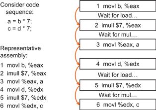
FIGURE 5.14 In-Order Execution.
An out-of-order processor allows independent instructions to execute out of order as long as the instruction’s dependencies have been fulfilled. On an out-of-order processor with sufficient execution resources the instruction schedule is more efficient. Instruction 4 can execute at the same time as instruction 1. Instruction 5 can execute at the same time as instruction 2. Instruction 6 can execute at the same time as instruction 3. The results are still written in program order; however, superscalar execution enables more efficient usage of process resources.
This is a fundamental difference between the Intel Atom processor and other modern out-of-order processors. One method of addressing this disadvantage is to use a compiler that schedules for the Intel Atom processor. If the compiler laid out the instructions in the order specified in Figure 5.15, many of the same benefits of out-of-order execution would result when executing on the Intel Atom processor.

FIGURE 5.15 Instruction Schedule for In-Order Execution.
Front End
The components that comprise what is termed the front end of the processor are charged with finding and placing the instructions into the execution units. The components that comprise the front end of the processor and their functionality are the following:
• Branch Prediction Unit. Predicts the target address for branches.
• Instruction TLB. Translates virtual to physical addresses.
• Instruction Cache. Fast access to recently executed instructions.
• Prefetch Buffer. Holds instruction bytes ready for decoding.
The front end of the microarchitecture performs the instruction fetch and instruction issue phases of the pipeline. The first action in placing an instruction into the pipeline is to obtain the address of the instruction. This address comes from one of two places. If the current instruction that is just entering the pipeline is not a branch instruction, the next instruction is equal to the address of the current instruction plus the size of the current instruction. If the current instruction is a branch, the next instruction is determined by the branch prediction unit that caches previously seen branches and provides a prediction as to the direction and target of the branch. The instruction TLB translates the virtual address used by the program into the physical address where the instruction is actually stored. The instruction cache is used to keep recently executed instructions closer to the processor if those particular instructions are executed again. The instruction cache is 24 kB.
Predecode Bits
The instruction cache contains predecode bits to demarcate individual instructions to improve decode speed. One of the challenges with the IA-32 and Intel 64 ISA is that instructions are variable in length. In other words, the size of the instruction is not known until the instruction has been partially decoded. The front end contains two instruction decoders that enable up to two instructions to be decoded per cycle, and this is consistent with the Intel Atom processor’s dual instruction execution architecture. These decoders assume the boundary of an instruction is known, which is a change from previous decoders used in Intel architecture processors. Previous processors buffered bytes into a window that was rotated from instruction to instruction. The front end also contains two queues to temporarily hold decoded instructions until they are ready to execute. Two queues service the two threads of execution available due to support for Intel Hyper-Threading Technology.
Instruction Decode
During instruction decode, the IA-32 and Intel 64 instructions are decoded into another instruction that drives the microarchitecture. In previous IA-32 and Intel 64 architecture processors, the decode phase broke instructions into micro-operations characterized as very simple. For example, an addition operation that referenced and wrote to memory would be broken down into four micro-operations for execution by the microarchitecture. In the Intel Atom processor, the two decoders are capable of decoding most instructions in the Intel 64 and IA-32 architecture. The microarchitecture does make a distinction between instructions that are too complicated to execute in the pipeline and simpler instructions, and has a fallback mechanism, a microcode sequencer. The microcode sequencer is used to decode the more complex instructions into a number of smaller operations for execution in the pipeline. The drawback to the microcode store is that these instructions decode slower and break down into more than one operation in the pipeline.
Decode Stage to Issue Stage
The decode stages can decode up to two instructions to keep the two-issue pipeline filled; however, in some cases the decoder is limited in only being able to decode one instruction per cycle. Cases where the decoder is limited to one instruction per cycle include x87 floating-point instructions and branch instructions. The Intel Atom processor is dual-issue superscalar, but it is not perfectly symmetrical. Not every possible pairing of operations can execute in the pipeline at the same time. The instruction queue holds instructions until they are ready to execute in the memory execution cluster, the integer execution cluster, or the FP/SIMD execution cluster.
Memory Execution Cluster
The memory execution cluster provides the functionality for generating addresses and accessing data. Components of the memory execution cluster and their functionality include the following:
• Address Generation Unit. Generates data address composing base address, scale, and offset.
• Data TLB. Translates virtual address to physical address.
• Data Cache. Holds recently accessed data.
• Prefetcher. Predicts future access and fetches by analyzing previous accesses.
• Write-Combining Buffers. Allows grouping of individual write operations before being sent on to the cache; enables more efficient memory bandwidth utilization.
In the optimum case for a data access, the data are resident in the L1 cache; however, if the data are not resident there, an L2 cache request is made. One architectural optimization is the inclusion of a data prefetcher that analyzes historical access patterns and attempts to fetch future data in advance of reference.
Common to many architectures, the memory subsystem supports store forwarding, which takes a result of a previous store and forwards the value internally for use in a proceeding load operation. This forwarding eliminates potential pipeline stalls because the load instruction does not need to wait until the stored value is committed to the cache. A special case of forwarding results from operations that affect the flags and instructions dependent upon them. Branch operations have an implicit one-cycle penalty. All other instructions have a two-cycle bubble.
One common occurrence in instruction sequences is the computation of an address for use in subsequent instructions. For example, Figure 5.16 shows an instruction sequence where the second instruction depends on an address calculation from the previous instruction. This dependency would cause a three-cycle stall because the second instruction cannot execute until the result of the first instruction is known. Figure 5.16 shows the impact on the pipeline as there is a bubble between the AG and EX pipeline stages.
![]()
FIGURE 5.16 Address Generation Stall.
Integer Execution Cluster
The integer execution cluster features two arithmetic/logic units (ALU) enabling joint execution of many instructions. Dual execution in the execution cluster has some limitations.
FP/SIMD Execution Cluster
The floating-point execution cluster executes x87, SIMD, and integer multiply instructions. The cluster contains two ALUs and supports limited combinations of dual execution. The second execution unit is limited to floating-point additions. Integer multiplies take more than one cycle in the execute stage and effectively stall subsequent instructions until after the multiply is finished with the execute stage. The only exceptions to this are for subsequent integer multiplies, which can be effectively pipelined in this stage.
Safe Instruction Recognition
One microarchitectural issue specific to the Intel Atom processor is that the integer pipeline is shorter than the floating-point pipeline. Floating-point exceptions can occur in an instruction that is programmatically before an integer instruction, but takes longer to retire. A straightforward solution would be to delay retirement of integer instructions until preceding floating-point instructions in the pipeline retire. This solution would effectively add a multicycle delay to integer instruction retirement. Instead, a safe instruction recognition algorithm is employed that detects whether it is possible for a floating-point instruction to fault. In only those cases, a restart of preceding integer instructions from the scheduler would be issued.
Bus Cluster
The bus cluster is the connection from the processor to the memory subsystem and contains a 512-kB, eight-way L2 cache. The bus cluster also contains the Bus Interface Unit (BIU) and Advanced Programmable Interrupt Controller (APIC).