
Chapter 17
Platform Debug
Once you eliminate the impossible, whatever remains, no matter how improbable, must be the truth.
—Sir Arthur Conan Doyle
The rapid pace of innovation in the development of embedded systems can be exhilarating, but it is not without its consequences for developers. Balancing the thrill of working with new processors, sensors, and circuit boards is the fact that new hardware, like new software, is often buggy. Moreover, new hardware platforms and system software have the unique characteristic of failing in ways that stable systems do not. Application-level software developers targeting general-purpose computers are not typically accustomed to hardware or system-level faults; when they debug errors, they know the problem lies within the bounds of their application development environment. Not so with embedded systems.
When developing an embedded system, it is highly likely that most aspects of the system will be reused from a previous one. This is important because developing new software on new hardware can be a challenging task, because when things break there are many possible culprits. When some portions of the system are stable and known to function, whether it is software, like the OS kernel or a previous device driver implementation, or hardware, such as a circuit board layout that is known to be correctly implemented, these likely correct components can be used to help eliminate debug targets and hence reduce the subsets of the system that must be systematically examined for correct function.
In this chapter, we will explore a process for debugging an embedded platform. As we will see, platform debug is more art than well-defined process, but after working through the chapter, you should be capable of diagnosing and identifying the most important classes of errors that, for example, keep embedded systems from booting correctly to an operating system.
To do so, we will first discuss a perspective and methodology that form the foundation for debugging an embedded platform. Then, we will discuss the tools and chipset features that aid and enable debugging. Finally, we will consider the platform debug process in detail.
Debugging New Platforms
Suppose you are one of a small number of embedded systems engineers who have formed a startup company around your new embedded device concept. The team has completed its first circuit board design, and a fully built-out board—including the Intel® Atom™ processor and all the burnt-in components—has been delivered from the third-party vendor, and it is time for first boot. It is a Linux-based platform, and the system has been designed to boot from a USB device. The team assembles, the USB memory stick is inserted, power is turned on, and … nothing. No flashing LEDs, no indicators of any kind. The team was expecting a celebration, but got nothing but inert disappointment. What’s wrong? Is the problem serious or trivial? How will you know?
Of course, in this fictional scenario and in every other real-world platform debug effort, there are an extraordinary number of possible causes. Was the power supply plugged in? Was memory inserted and properly seated? Is some component configured for debugging rather than operation? Is there a short on the circuit board? The fully enumerated list would be a very long one, indeed. Rather than working with a flat checklist, however, we will follow a process, one that is designed to systematically identify what works and what is faulty or misconfigured.
Before jumping in, it will be constructive to consider your mindset and perspective as you debug. Debugging is an open-ended activity, in which neither the ultimate explanation nor the time that will be needed to find it is known in advance. What is certain, however, is that you must ultimately find the problem. Given this, for most it is highly productive to adopt a positive, inquisitive mindset as you begin debugging. Not only will this make you feel better as you work, but it will make you better at what you are trying to do. Debugging, whether at the platform level or the application level, requires a careful, systematic effort to reduce possible causes until the problem is identified. Debugging in frustration or in haste is not conducive to careful, systematic work. So, before you start debugging, make sure you begin with the right frame of mind: be calm, systematic, and curious.
A Process for Debugging a New Platform
The modify-compile-debug pattern so familiar to programmers is of little use when your platform will not boot. This traditional practice is a productive one, because with each change there is a high probability that any problems observed in the newly compiled program will be related to the most recent changes. When a system will not boot, while there is a possibility that only a small number of changes have been made that help to locate the source of the failure (that is, “all we changed was the power supply!”), but it is more likely that trouble with a brand new embedded system cannot a priori be confined to a small set of locations.
To tackle the search systematically, you can rely upon a structure process like the one presented in this chapter. The process can be characterized in three high-level steps:
1. Visual examination. Look at the system. Verify that external cords, cables, and I/O devices are attached. Remove the cover and examine the circuit board for damage and properly seated components.
2. Hardware evaluation. Are the hardware components, such as power supplies, voltage regulators, and integrated circuits, in their proper state and operating normally? As we will see, this step is subdivided into a number of specific, ordered substeps to uncover possible hardware faults or misconfigurations.
3. Software evaluation. Are the BIOS and OS kernel properly configured and able to boot? Are you aware of all known bugs from the most recent data sheet? Once the hardware has been determined to be operating properly, the next step is to verify that the systems software is properly configured and is being invoked correctly. This step, too, is subdivided into further substeps.
These three steps are illustrated in an overall platform debug flowchart in Figure 17.1. We will soon discuss these debug steps in detail, but before doing so we must first review some tools and chipset features essential to platform debug.

FIGURE 17.1 Platform Debug Process.
Debug Tools and Chipset Features
Debugging at the platform level requires inspection of system state that is not typically visible to the user or programmer. Consequently, a variety of tools may be needed in the course of a debugging session. In this section, we will discuss the classes of tools that are typically employed in the platform debug process. These include both hardware probes and analyzers and software tools.
Additionally, we will discuss some processor and chipset features that provide access to internal chip state for the purposes of debug and test that would otherwise be inaccessible.
Observing the output characteristics of hardware devices implies the measurement of fundamental electrical characteristics such as voltage and current. While voltmeters and multimeters can offer such measurements, it is typically necessary to observe these characteristics as they change through time.
To do this, hardware probes are required. Such probes come in several varieties and device specializations. Regardless of the power levels and time domains in which your system operates, hardware probes have been produced to meet your needs. Often, however, extremes of both very high and very low power and frequency come at a steep price. For most classes of embedded systems, however, reasonably affordable, USB-based measurement devices can be obtained in the cost range of hundreds of dollars (USD). At the high end, some probes can cost hundreds of thousands of dollars. Most university and digital design laboratories will be stocked with these devices.
Oscilloscopes
Oscilloscopes are a ubiquitous form of hardware probe that primarily provides voltage levels as a function of time for one or more inputs. For example, leads can be attached to CPU pins to watch the change in voltage level as power is applied to a system. This simple example illustrates the type of observation required to verify that the various power levels required by a CPU are being provided and are arriving in the correct order.
Logic Analyzers
Logic analyzers are a related form of hardware probe whose purpose is to capture hardware protocol-level information being communicated across one or more connections. While oscilloscopes report analog values, logic analyzers are designed to work with digital systems, where information and system state are expressed at discrete voltage levels.
The user of the probe has complete control over how the logic analyzer is used. The user chooses the points of observation within the system under test, provides names for the input signals, and then expresses when information should be captured in terms of the values observed among the input signals. In this way, a logic analyzer can be programmed to observe a precise subset of system state under specific system conditions. Logic analyzers, like oscilloscopes, come in a variety of forms, from stand-alone units to more modest USB-based ones.
As an example, a logic analyzer can be used to capture a trace of memory addresses that are transmitted between a CPU and DRAM. For a given application, a logic analyzer must be capable of capturing the required number of inputs (for example, one for each pin under observation) and must operate at an adequate frequency to observe the state transitions on the pins.
Bus Analyzers
Important computer I/O bus types, such as PCI Express™, are popular enough to warrant their own logic analyzer specialization. A PCI Express bus analyzer can capture and analyze PCI traffic in a much more straightforward way than a comparably capable logic analyzer would. Logic analyzers are generally more expensive, but also may be widely applicable.
Power-On Self-Test (POST) Cards
In IA-32-based devices, power-on self-test (POST) routines run immediately after power is applied to the system. These routines are defined by the BIOS vendor and are the part of the pre-boot sequence intended to catalog system resources and identify easily recognizable classes of system errors.
PC users may be familiar with the so-called “beep codes” that can be used to diagnose some hardware problems during system boot. For example, booting a PC with heavy book on the keyboard (which presses down multiple keys continuously) will, in many machines, result in a sustained series of beeps as the system boots.
In addition to reporting errors through the system speaker, most BIOS vendors report error numbers through I/O port 0x80, which is mapped to a PCI location that can be observed by a PCI card. These cards, sometimes called POST cards or port 80 cards, can be used to collect a finer grain of BIOS-defined error conditions.
JTAG Adapters
The Joint Test Action Group, or JTAG, standard defines a process for testing boards and controlling processor execution. A CPU or chipset supporting JTAG must support a minimum set of commands to reset the system, read and write system state, and read and write test data. The most basic usage is to send test vectors into a system via the JTAG interface. Such an interaction can be used to test logic correctness that cannot be definitively verified in pre-silicon simulation.
In addition to system test, the JTAG interface and command set can be used to control the CPU and its software. In this context, JTAG can be used as a systems-level debugger, enabling breakpoints, stepping, and source code correlation at the systems software level. JTAG can also be used to initialize devices or program a boot loader into ROM for systems that are powering up for the first time and do not have code in ROM to control the boot sequence. As a debug interface, JTAG can be invaluable because it is available regardless of the soft state of the system.
A JTAG adapter connects to the system under test via the JTAG interface and through a debug machine through some other interface, such as USB.
Most chip vendors provide their own extended version of JTAG. Intel processors, including Intel Atom, feature extended debug ports (XDP), which implement JTAG and some proprietary extensions.
Debug Process Details
Given the preceding high-level overview and discussion of tools, we are now ready to consider the steps of the platform debug process in detail.
Visual Examination
The first step of the process, visual examination, is at once the most obvious and the least familiar of the steps in the platform debug process. The step is unfamiliar because most software-level debugging can be carried out in ignorance of the physical state of the computing device. New embedded systems, and new digital systems of all kinds, must be methodically examined for physical correctness and proper component inventory.
Depending on the enclosure, removing covers to get at the underlying circuit board may be a challenge in and of itself. Sometimes rare screw heads are used, requiring rare screwdrivers; other times, no screws are used at all and the proper sequence of squeezes, pressures, and pries must be applied to separate pieces of an enclosure.
Assuming that the circuit board can be uncovered, the next step is to take a physical inventory of proper components while noting signs of physical damage. It is certainly possible for assemblers to leave pieces out, use the wrong pieces, or accidentally damage components or metal traces during assembly. If the design includes jumpers or other forms of switches, verify that they are in their proper state for system boot.
During the visual examination, signs of shorts or burning should be noted as well. Faulty design and components can lead to shorts or exceeded capacity, resulting in burnt-out, broken components and devices.
Ensure that all cabling, both power and I/O, is properly seated and interconnected. For components that include visible or audible cues, such as LEDs or fans, take note of what functional indicators are present during an attempted boot. These indicators, when present, can dramatically shorten the time needed to identify where in the system boot process failure occurs.
Hardware Evaluation
After a successful visual examination, the next step is to examine the state of the hardware components and to observe their proper operation through time. The high-level steps of this process are illustrated in Figure 17.2 and elaborated on below.

FIGURE 17.2 Steps in Hardware Evaluation.
Verify Real-Time Clock. Computing devices built around the Intel architecture generally include a 3.3 V lithium battery to power a real-time clock (RTC). If this battery is missing, damaged, or dead, the system will not come out of reset. You can verify that the RTC is operating properly by examining the SUSCLK signal from the I/O controller hub (ICH) RTC oscillator circuit. This signal should exhibit a square waveform at 32 kHz.
Since the RTC logic is stateful, it is also good practice to remove the battery and reinsert it to return to a known starting state when experiencing problems booting or resetting platform.
Source Power Available. Most Intel architecture systems included ATX power supplies. The ATX power supply will provide DC power at several voltage levels from an AC wall outlet. The ATX signal PS_ON# indicates that the power supply should supply the voltage levels and the power supply will assert the PWR_OK signal when all voltages are available and stable.
The voltage levels are provided in sequence from high to low, as indicated in Figure 17.3. The timings T1, T2, and T3 are specific to the power supply vendor and can be found in the supply’s datasheet.

FIGURE 17.3 ATX Power Supply Timing Diagram—Timings T1, T2, and T3 Are Model Specific.
Voltage Levels Stable. Once the power supply is verified to be providing power, the next step is to determine whether the chipset is powering on with properly conditioned standby voltage levels. The detailed levels and timings are specific to a PCH or system-on-chip device, but a representative illustration is provided in Figure 17.4.
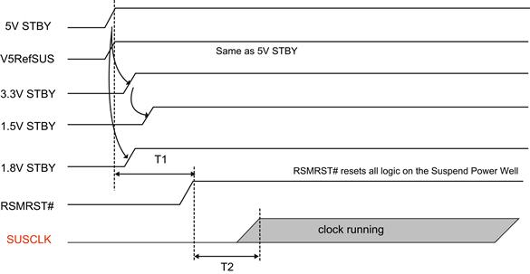
FIGURE 17.4 Representative PCH Power-On Timing Diagram.
At this point in the boot process, the system is in the S5 system sleep state. The RTC is running, but the system itself is not operating. To begin wakeup, an external event such as a power button press is required.
Given that the system is in a proper standby state, a power button press will transition the system from S5 ultimately to S0. Along the way, the chipset will assert the PS_ON# signal to turn on the ATX power supply. The specific timings between these events are, as expected, chipset specific, but a representative illustration of the relative timing can be found in Figure 17.5.
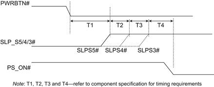
FIGURE 17.5 Power-On Signal Timing.
There is an additional signal, SKTOCC#, which indicates whether a CPU is found in the CPU socket. If the socket is empty or if the chip is improperly seated, this signal will not be deasserted and neither will PS_ON#.
Regardless of the chipset and CPU in your design, voltage regulators and their associate status signals will be present to ensure proper levels before the system attempts to generate and apply the core CPU voltage. There will be a signal named something along the lines of VCCP_PGOOD to indicate that the core voltage, VCC_CPU, is available and properly conditioned.
Clocks Running. Once the power supplies are known to be stable, the next milestone is to verify that the system clocks are operating correctly. Intel architecture devices will feature a clock chip for the CPU (for example, CK505) and chipset and one or more clock chips for I/O devices (for example, DB1200).
The CPU frequency is indicated by the BSEL clock chip input signals. The BSEL signals and the resulting clock source outputs can be examined for correct signal timing. For design-specific clock distribution problems, timing can be checked at clock signal termination points.
Devices and CPU Reset. If power and clock signals are present and stable, the PCH will attempt a system reset to bring all devices into an operating state. After PWR_OK is asserted, the PCH will assert PLTRST#. Then the PCH will send a CPU reset packet. Once that message is acknowledged, CPURST# will be deasserted, and this will cause the CPU to begin executing at its reset vector, physical address 0xFFFFFFF0. If your system gets this far, it is ready to begin executing its first instruction.
Software Evaluation
If the hardware is in order and the system will not boot properly, the next step is to check the software configuration of the platform. This includes the BIOS settings, which affect the pre-boot operation of the device, as well as the OS itself.
As the CPU leaves the reset stage, it will fetch and execute from the reset vector, physical address 0xFFFFFFF0. This address will be mapped to firmware or an I/O device, depending on the BIOS boot settings. A normal boot sequence will proceed as described in Chapter 6.
To diagnose problems during the BIOS phase of system boot, BIOS vendors output POST codes as described previously. These codes indicate which steps of the boot process are working properly and which step hangs the system. POST codes can be observed via PCI cards or via LEDs built into the platform. Figure 17.6 provides an example of a generic boot sequence and associated POST codes. Specific examples of POST codes can be found in vendor-provided BIOS documentation.
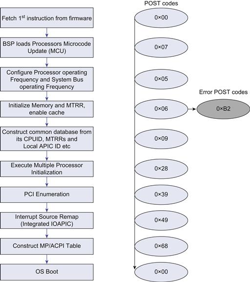
FIGURE 17.6 Power-On Signal Timing for AMI BIOS.
At this stage, it is important to verify that the BIOS version is correct and that the BIOS boot and configuration options are appropriate for the system under test.
If the system boots properly to this point, you have successfully transitioned from platform debug to operating system or device driver debug.
Additional Resources
This brief chapter has merely scratched the surface with respect to what can be said about debugging new and faulty hardware platforms. Of course, there is no better way to learn platform debugging skills than to learn from experienced engineers.
The Intel Embedded Design Center hosts a growing number of experience reports describing both specific and general examples of debugging platforms and specific hardware faults.
Table 17.1 lists a few pointers that are available at this time. There is a growing list of such articles on the Intel web site and other places, and there is a reasonable probability that problems you may be encountering with your embedded system have been found and written about by others.
Table 17.1. Further Platform Debug Resources
| Title | URL |
| Debug Methodology for Intel Architecture-Based Platforms | http://download.intel.com/design/intarch/papers/321053.pdf |
| Processor Reorder Buffer (ROB) Timeout | http://download.intel.com/design/intarch/papers/324353.pdf |
| Debugging Machine Check Exceptions on Embedded IA Platforms | http://edc.intel.com/Link.aspx?id=3565 |
In fact, if you find that you have stumbled upon a seemingly unique platform error, you should be sure to write it up for the benefit of your fellow engineers!
Summary
In this chapter, we have explored the basics of platform-level debugging. Debugging a brand-new hardware design is a necessarily open-ended activity. Through rigorous design and careful simulation, many system errors can be avoided. However, not all faults and errors can be designed around, so embedded systems engineers need to be prepared to debug a system with very few preconceived notions about what operates correctly.
Of paramount concern is your frame of mind as you begin debugging. Careful, methodical evaluation is needed for productive platform debug, and hasty action and poor documentation are counterproductive in this context.
This chapter has introduced a simple process for system-level platform debugging. Through visual examination of the system components and a careful walk-through of the hardware and software boot sequences, it should be possible to pinpoint the source of platform boot errors through systematic trial and observation.