Chapter 6
Photovoltaic Systems
6.1 PV Solar Cells and Solar Module
In photovoltaic energy systems, the solar energy (mainly sunlight) is directly converted to electric energy using photovoltaic solar cell modules. They have no moving parts, therefore require little maintenance. The basic principle of photovoltaic effect was discovered by Becquerel in 1839 using selenium. He discovered photovoltaic effect at a junction between a semiconductor (selenium) and an electrolyte. But it was not considered for power generation until 1954 when silicon semiconductors became available, and PV solar cells based on semiconductor technology were developed. Selenium and silicon are both semiconductor materials, but it was only when the three researchers, Gerald Pearson, Daryl Chapin and Calvin Fuller, at Bell Laboratories discovered a silicon solar cell, which was the first material to directly convert enough sunlight into electricity to run electrical devices. The efficiency of the silicon solar cell, which was produced at Bell Laboratories, was only 4%.
In most of today's solar cells, the absorption of photons, which results in the generation of the charge carriers, and the subsequent separation of the photo-generated charge carriers take place in semiconductor materials. A semiconductor is a material that has an electrical property which lies in between that of a conductor and an insulator. The semiconductor materials commonly used now are silicon and germanium. However, the availability of silicon in abundance has made it more commonly used semiconductor material. Solar cells using silicon were first produced in 1954. They found their immediate application in space activities. Their first use was to power a small radio transmitter in the US space satellite Vanguard I. Now almost in all spacecraft, the power source is PV cells.
Photovoltaic power is one of the fastest growing renewable energy technologies. Annual production of PV cells grew tenfold from about 50 MW in 1990 to more than 500 MW by 2003. Rapid progress in increasing the efficiency and reducing the cost of PV cells has been made over the past few decades [1]. Their uses are now widespread in domestic, commercial and industrial buildings.
A brief description of semiconductors and their properties is given here to understand the basics of energy conversion.
6.1.1 Semiconductor Technology
In semiconductors, there is an energy gap between the valence band and the conduction band but the energy gap is not very large. These materials therefore have properties between those of a conductor and an insulator. Due to a number of favourable characteristics, silicon is the solar industry's most common semiconductor material. However, in its pure crystalline form, silicon is a poor conductor of electricity as it has equal number of free electrons and holes. In order to make the silicon material suitable for an electronic or solar application, impurity atoms are added to crystalline silicon. This process is known as doping. The doped semiconductor is called extrinsic semiconductor. The impurities that are added are boron, gallium, aluminium or phosphorous, arsenic or antimony. Silicon is a group IV element on the periodic chart and has four electrons in its outermost shell. When silicon is doped with group V element such as arsenic (As), or phosphorous, its atoms replace silicon atoms at a small number of points on the crystal lattice. Since their atom has five electrons in its outer shell, an extra electron is added to the crystal. This extra electron (often called a donor electron) is easily excited into the conduction band as a freely moving current carrier. Silicon can also be doped with an element from group III of the periodic table, such as gallium (Ga), boron or aluminium. In case silicon is doped with gallium or aluminium, the impurity has only three electrons in its outermost shell, so there is a deficiency of one electron at every point where a gallium/aluminium atom replaces a silicon atom. The gallium often takes an electron from a neighbouring silicon atom leaving a “hole” or empty state in the valence band of the silicon. This “hole” is free to roam around in the valence band and effectively acts as a positive charge carrier. The electrons move forward to fill up the spaces (holes) in front of them and create another space behind them. The holes move in the direction opposite of electrons; hence, they behave as a positive charge. Thus, doping with group III elements produces a p-type semiconductor because the effective charge carriers (holes) are positive. On the other hand, doping with group V elements results in an n-type semiconductor since the charge carriers (electrons) are negative.
A PV cell consists primarily of two layers of semiconductor material, which create a p–n junction. In a p–n junction, one layer of negatively doped material is connected physically to another layer of positively doped material. The two layers are connected together by a flat surface, allowing as much surface area contact as possible. When a junction between p- and n-type materials is formed, the carriers (free electrons and holes) diffuse from a higher concentration side to the lower concentration side. For generating electricity, the negative side, or the side having excess electrons, is faced towards the source of light while the positive side is faced away. When light strikes the surface of the negative side of the PV cell, the photons begin striking the electron shells of the PV-cell material. The semiconductor material absorbs photons with energies equal to or greater than its band gap. Due to photon absorption, an electron of the valence band is promoted to the conduction band and is free to move through, becoming a free-roaming electron. The positive layer of the material being so close in proximity combined with the abundance of electrons in the negative layer forces the electron towards the positive side of the PV cell. However, once on the positive side, the electron is unable to return to its original parent atom and, as a result, is stuck on the positive side of the cell. In order for this free charge to be captured for current generation, decay to the lower energy state, that is, recombination with the hole in the valence band, has to be prevented through charge separation. Thus, an electron–hole pair is produced. The energy available in the photon is given by
where h is Planck's constant = ![]() , c is the speed of light, λ is the wavelength of photons in metres. For energies of photons less than the band gap energy, no absorption takes place. For photons having energy much more than the band gap energy, still only one electron–hole pair is generated and the remaining energy is wasted as heat. One of the most critical requirements for a single-junction cell is that the band gap energy must be optimized to transfer maximum energy from the incident light to the photo-generated electron–hole pairs.
, c is the speed of light, λ is the wavelength of photons in metres. For energies of photons less than the band gap energy, no absorption takes place. For photons having energy much more than the band gap energy, still only one electron–hole pair is generated and the remaining energy is wasted as heat. One of the most critical requirements for a single-junction cell is that the band gap energy must be optimized to transfer maximum energy from the incident light to the photo-generated electron–hole pairs.
Because the efficiency depends on the product of open-circuit voltage (![]() ) and short-circuit current (
) and short-circuit current (![]() ), there is an optimum energy band gap for producing maximum efficiency of PV cells. It has been found that the optimum energy band gap of 1.5 eV is ideal for solar power generation. In practice, semiconductors with energy band gaps in the range of 1.0–1.7 eV are used.
), there is an optimum energy band gap for producing maximum efficiency of PV cells. It has been found that the optimum energy band gap of 1.5 eV is ideal for solar power generation. In practice, semiconductors with energy band gaps in the range of 1.0–1.7 eV are used.
The band gap energy of silicon (1.12 eV) is almost ideal and allows absorption of photons in the near-infrared (NIR), visible and ultraviolet spectrum [2, 3]. Silicon has an indirect energy band gap of approximately 1.1 eV at room temperature. The indirect energy band gap results in a low optical absorption coefficient (α ≤ 104 cm−1) for photons with energies below 3.4 eV, and this means that the silicon must be 100–300 µm thick for achieving efficient light absorption. The electron–hole pairs generated by the light should be able to diffuse up to that distance to reach the electric field in the depletion region of the junction if they are to contribute to the photocurrent. (Increasing w to more than a few microns by lowering the doping concentrations is at the expense of increasing the device series resistance to the point where it severely degrades the device efficiency.)
Today's most successful materials for thin-film photovoltaics are α-Si, where the optical absorption is increased by impurity scattering. Cadmium telluride (CdTe), with a band gap of 1.48 eV, and copper indium gallium selenide (CIGS), whose band can be tuned around the nominal value of 1.04 eV by controlling its composition and which has the highest absorption constant of 3-6 × 105 cm−1 reported for any semiconductor, are now favourite materials.
6.2 Solar Cell Characteristics
An ideal solar cell can be modelled as a current source in parallel with a diode. When there is no light present to generate any current, the PV cell behaves as a diode. As the intensity of incident light increases, current is generated by the PV cell, as illustrated in Fig. 6.1. The diode current (when the junction is not illuminated) is given by

where ![]() is the reverse saturation current;
is the reverse saturation current; ![]() is 1.38 × 10⁻²³ T, where T is the cell temperature in Kelvin; and V is the measured cell voltage.
is 1.38 × 10⁻²³ T, where T is the cell temperature in Kelvin; and V is the measured cell voltage.

Figure 6.1 Solar cell characteristics.
When the p–n junction is illuminated, the cell current is given by, the total current I equal to the current ![]() generated by the photoelectric effect minus the diode current
generated by the photoelectric effect minus the diode current ![]() , according to Eq. (6.2):
, according to Eq. (6.2):

As shown in Fig. 6.2, the short-circuit current ![]() corresponds to the short-circuit condition when the impedance is low and is calculated when the voltage equals 0.
corresponds to the short-circuit condition when the impedance is low and is calculated when the voltage equals 0.

Figure 6.2 Equivalent circuit of solar cell under light; (a) ideal cell, (b) real cell.
The open-circuit voltage (![]() ) occurs when there is no current passing through the cell.
) occurs when there is no current passing through the cell.
![]() is also the maximum voltage difference across the cell for a forward-bias power quadrant.
is also the maximum voltage difference across the cell for a forward-bias power quadrant.
![]() for forward-bias power quadrant.
for forward-bias power quadrant.
![]() occurs at the beginning of the forward-bias sweep and is the maximum current value in the power quadrant. For an ideal cell, this maximum current value is the total current produced in the solar cell by photon excitation.
occurs at the beginning of the forward-bias sweep and is the maximum current value in the power quadrant. For an ideal cell, this maximum current value is the total current produced in the solar cell by photon excitation.
![]() for forward-bias power quadrant.
for forward-bias power quadrant.
The power produced by the cell in Watts can be easily calculated by the equation P = IV. At the ![]() and
and ![]() points, the power will be zero and the maximum value for power will occur between the two. The voltage and current at this maximum power point (MPP) are denoted as
points, the power will be zero and the maximum value for power will occur between the two. The voltage and current at this maximum power point (MPP) are denoted as ![]() and
and ![]() , respectively.
, respectively.
6.2.1 Equivalent Circuit
The solar cell can be seen as a current generator which generates the current ![]() . The dark current
. The dark current ![]() flows in the opposite direction and is caused by a potential between the +ve and –ve terminals. In addition, there are two resistances: one in series (Rs) and the other in parallel (Rsh). The series resistance is caused by the fact that a solar cell is not a perfect conductor. The parallel resistance is caused by leakage of current from one terminal to the other due to poor insulation. In an ideal solar cell, Rs = 0 and Rsh = ∞. The equivalent circuit of an ideal cell and practical cell (including all resistances) is shown in Fig. 6.2.
flows in the opposite direction and is caused by a potential between the +ve and –ve terminals. In addition, there are two resistances: one in series (Rs) and the other in parallel (Rsh). The series resistance is caused by the fact that a solar cell is not a perfect conductor. The parallel resistance is caused by leakage of current from one terminal to the other due to poor insulation. In an ideal solar cell, Rs = 0 and Rsh = ∞. The equivalent circuit of an ideal cell and practical cell (including all resistances) is shown in Fig. 6.2.
The equation for load current of the practical cell from the equivalent circuit is

A shunt resistance Rsh of a few hundred ohms does not reduce the output power of the solar cell appreciably. In reality, Rsh is much larger than a few hundred ohms and can in most cases be neglected. The series resistance, however, can drastically reduce the output power. For example, a series resistance of only 5 Ω can reduce the output power by 30%.
6.2.2 Solar PV Module
Since the total power available from single solar cell is very small, it cannot be utilized for any useful work. Individual solar cells are usually manufactured and combined into modules that consist of 36 cells (12 V) to 72 cells (24 V) depending on the output voltage and current of the module. When a module is connected to a system, an important consideration is the behaviour of the module when it is not illuminated. During night time, when none of the cells is generating photocurrent, the module may be considered as a series connection of diodes that may be forward biased by the storage batteries. This will result in leakage current through the diodes and discharging of batteries.
Another consideration in series connection of solar cells relates to the shading of individual cells. If any cell of the module is shaded, it will not produce any current. Since the cells are connected in series, it may become forward biased if other unshaded modules are connected in parallel. This will result in heating of the shadowed cell and may damage the module.
When cells are mounted in modules, the unit is fixed on a durable back cover with a transparent cover on the top and hermetically sealed to make it suitable for outdoor applications. The modules vary in size according to the manufacturers but are typically between 0.5 and 1 m2 and generate around 100 W/m2 of energy under peak solar conditions for a 10% efficient module.
6.2.3 Series and Parallel Connections of Cells
In order to obtain higher current and voltage output, cells are connected together in a module. To increase the voltage of the module, cells are connected together in series, and to increase the current, cells are connected in parallel. How many cells are to be connected in series or in parallel is determined by the desired string or module output. When cells are connected in a series, the voltage of the entire string is the sum of the individual cells' voltages as shown in Eq. (6.7) for two cells. The total current of the string is equal to the current of one cell in the string, as shown in Eq. (6.8).
or
Alternatively, when cells are connected in parallel, the currents add and the voltages are equal as seen in Eq. (6.9) and (6.10). The I-V curve of two cells connected in parallel is shown in Fig. 6.3. The current of the combined curve is equal to the sum of the two currents at a specific voltage.

Figure 6.3 I-V curve of two cells connected in parallel.
Unfortunately, it is very difficult to get two identical cells in reality. In addition, cell mismatch occurs when a cell in a series connected string is shaded or damaged preventing it from generating current equal to the other cells in the string. This mismatch results in degradation to the module and a lower power output.
When two cells with mismatched characteristics are connected in series, the composite characteristics can be obtained by using the individual output voltage of the cell corresponding to common current, for all operating points as shown in Fig. 6.4. Cell mismatch has a substantial effect on the I-V curve of the whole module. A cell with a current output lower than that of the rest of the cells in the string is referred to as a “weak cell”. When cells are connected in series, the total current is limited by the weakest cell while the voltages add as normal. The combined output of the cells is dependent on the reverse voltage behaviour of the weak cell. The effects of shading one cell in a series connection can be seen in Fig. 6.5. One cell in a series string of three cells is shaded 50%. This causes the current produced by this cell to drop by about 50%, and the current of the resultant curve drops similarly. The voltages of the three cells add while the current is limited by the weak shaded cell.

Figure 6.4 Series-connected cell.

Figure 6.5 The effect of mismatched series string of three cells with one cell shaded.
The short circuit is the worst-case condition for mismatched cells since it results in the reverse biasing of the weak cells. In open-circuit conditions, the cells are forward biased by their photo-generated currents. The shading of cell 2 results in it having a lower ![]() which ultimately lowers the
which ultimately lowers the ![]() of the combined cells. However, over a large number of cells, typically 36 in a module, this drop in Voc is not significant. A mismatched cell lowers the performance of the entire module by limiting the current output and slightly decreasing the VOC of the module.
of the combined cells. However, over a large number of cells, typically 36 in a module, this drop in Voc is not significant. A mismatched cell lowers the performance of the entire module by limiting the current output and slightly decreasing the VOC of the module.
6.2.4 Solar PV Panel
In a solar PV panel, several solar modules are connected in series/parallel as shown in Fig. 6.6. The panel contains a group of modules that can be wired and packaged off-site. When modules are connected in series, it is desirable to have each module produce maximum power at the same current. For parallelly connected modules, it is desirable to have each module produce maximum power at the same voltage.

Figure 6.6 Solar PV panel connected in series and parallel.
In parallel connection, blocking diodes are connected in series with each series string of modules as shown in Fig. 6.7. In a failed string, the voltage is lower than the normal string, and when the two are connected in parallel, the current will flow from the normal string to the failed string. The blocking diode will not allow the power absorption by the failed string from other strings. In addition, bypass diodes are connected across each module, so that if one module fails, the output of the remaining modules in a string will bypass the failed module.

Figure 6.7 Solar PV panel with blocking diodes.
6.2.5 PV Array
Because a single solar PV panel can only produce a limited amount of power, several panels are connected to form an array. A PV array is an interconnected system of PV modules that function as a single electricity-producing unit. In smaller systems, an array may consist of a single panel or for large systems may contain many panels connected together. The panels should be so installed that the shade of one panel must not fall on other panel throughout the year.
6.2.5.1 Design of PV System
The main aspect of interconnecting:
Suppose that the PV array comprises 16 modules of 160 W peak. The array peak power is 16 × 160 = 2.56 kW.
Taking the derating of array as 0.77, and daily sunshine hours of 6, the dc energy output of the array is ![]() .
.
If the power loss in dc cable is 3%, the total dc power output = ![]() , then the inverter power rating may be 11.5 kW.
, then the inverter power rating may be 11.5 kW.
Matching array voltage to the maximum and minimum inverter operating voltages:
Many of the inverters available will have a voltage operating window. When the temperature is at maximum, then the maximum power point (MPP) voltage of the array should never fall below the minimum operating value of the inverter.
If the ambient temperature is 35°C, the maximum temperature of the solar cell is 70°C. Now if the module used has rated MPP voltage of 35.4 V and voltage coefficient of –0.170 V/C, then the voltage at maximum temperature will be = ![]() . If voltage drop in dc cable is 3%, then the input voltage to the inverter at maximum temperature is
. If voltage drop in dc cable is 3%, then the input voltage to the inverter at maximum temperature is ![]() .
.
If the minimum voltage window of the inverter is 140 V, taking the factor of safety as 1.1, the minimum inverter voltage should be 154 V.
The minimum number of modules in a string can be 154/28.17 == 5.46, or 6 modules may be used. As the voltage of the cell increases, if the temperature falls from 25°C, the maximum voltage of the inverter window should be obtained for the place on the basis of the minimum temperature. If the effective temperature of the cell is taken as 25°C, then no voltage increase is required. The maximum number of modules for a 400 V inverter will be 400/29.05 = 13.76, or it can be 14.
Total number of modules required is 16 which may be connected in two strings of 8 modules.
6.3 Maximizing Power Output of PV Array
The output powers of photovoltaic (PV) panels have non-linear curves and depend on solar irradiance, degradation level and temperature. Their MPP changes non-linearly with environmental conditions and load profile. Since the photovoltaic electricity is expensive compared to the electricity from conventional sources, photovoltaic systems should be designed to operate at their maximum output power in any environmental conditions [4].
Two methods are generally used to increase the solar panel output power in photovoltaic systems. In the first one, the system will increase the incident solar irradiance on the solar panel. The system requires a sun tracker to track the Sun's position for increasing the received solar irradiance by the panels for different positions of the Sun. In that case, the environmental conditions define the quality of the generated power for each load. This method is used for medium- to high-scale photovoltaic systems and has a high cost. In the second method, solar panels are fixed and load profile is changed to maximize the power output under changing conditions of insolation and temperature. The maximum power is transferred to the load when the impedance of the source matches the load resistance. Therefore, in order to transfer maximum power from the panel to the load, the internal resistance of the panel has to match the load resistance as seen by the PV panel. For a fixed load, the equivalent resistance seen by the panel can be adjusted by changing the power converter duty cycle. To accomplish this objective, a switching converter is placed between the PV source and the load.
Tracking the MPP of a photovoltaic (PV) array is usually an essential part of a PV system. As such, many MPP tracking (MPPT) methods have been developed and implemented. With an MPPT control, it is possible to reach the output panel characteristics around the optimal power point. This method is utilized in small-scale photovoltaic applications. Combination of sun tracking or load matching and MPPT approaches can raise the energy output of a solar panel in photovoltaic systems.
6.3.1 Solar Tracking
Employing a tracking system with solar panel is one of the methods to increase the overall efficiency of the solar panel. Solar trackers are used to orient photovoltaic panels, reflectors, lenses or other optical devices towards the Sun. Since the Sun's position in the sky changes with the seasons and the time of day, trackers are used to align the collection system to maximize the power output. Solar tracking systems are of several types and can be classified according to several criteria. They can be classified depending on the number of rotation axes. Thus, solar tracking systems are with a single rotation axis or with two rotation axes. Since solar tracking involves moving parts which require a control, these are expensive. A single-axis tracking system is therefore the best solution for small PV power plants. Single-axis trackers will usually have a manual elevation (axis tilt) adjustment on the second axis depending on the different months in a year.
6.3.2 Design of Simple Automatic Solar Tracker
A simple cost-effective solar tracker can be constructed with the help of the following components.
- Photo transistor
- Voltage comparators
- dc motor
To track the Sun, the system should work in closed-loop form, and the controller needs to sense the light through a light sensor. Cadmium sulfide (CdS) photoresistor is used for tracking the Sun. The CdS photoresistor is a passive element that has a resistance inversely proportional to the amount of light (LDR) incident on it. To utilize the photoresistor, it is placed in series with another resistor. A voltage divider is thus formed at the junction between the photoresistor and another resistor shown in Fig. 6.8. The heart of the aforementioned circuit are two voltage comparators made using LM358 Dual Op-Amp. It is well known that when the intensity of light falling on an LDR increases, its resistance decreases. Here LDR is connected with a series resistor (R3 and R4); hence, when the intensity of light falling on an LDR increases, voltage across the corresponding resistor (R3 or R4) increases.
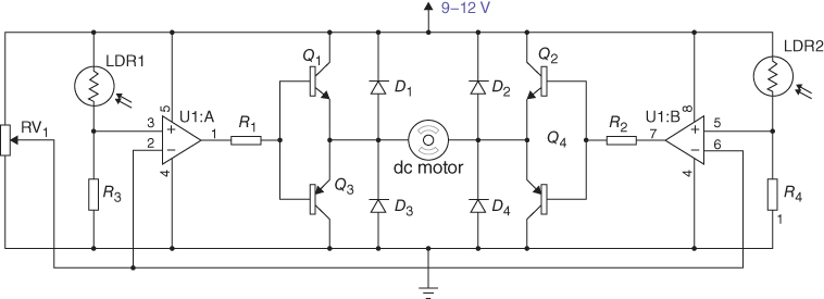
Figure 6.8 Simple automatic solar detector.
The output of the voltage comparator will be high when the voltage at the non-inverting terminal (+) is higher than the voltage at the inverting terminal (−). Inverting (−) terminals of both comparators are shorted and connected to a variable resistor (RV1), which is used to set the reference voltage. Thus, the sensitivity of both LDRs can be adjusted by varying the 10 K pot shown on the left side of the circuit diagram. When the light falls on an LDR increases, voltage at the non-inverting (+) terminal of the corresponding comparator increases and its output goes HIGH, as shown in Table 6.1.
Table 6.1 Rotation based on light
| Input A | Input B | Output C |
| 0 | 0 | STOP |
| 0 | 1 | CLOCKWISE |
| 1 | 0 | ANTI CLOCKWISE |
| 1 | 1 | STOP |
The direction of motor rotation is controlled by the H-bridge formed by the complimentary symmetry transistors BC547 and BC557. Consider the case when the output of the first comparator (U1:A) is high and the output of the second comparator (U1:B) is low. In this case, transistors Q1 and Q4 will turn on and the resulting current rotates the motor in clockwise direction. When the output of the first comparator is low and the output of the second comparator is high, transistors Q2 and Q3 will turns on and the resultant current rotates the motor in anticlockwise direction. If the outputs of both comparators are low, transistors Q3 and Q4 turn on, but no current will flow through the motor. Similarly, if the outputs of both comparators are high, transistors Q1 and Q2 turn on, but no current will flow through the motor. The dc motor should be connected to the panel in such a way that the rotation of the motor rotates the panel in the direction of movement of the Sun.
6.3.3 Load Matching for Optimal Operation
In order to obtain maximum power from an electrical circuit, the source impedance must be matched to the load impedance. A dc/dc converter acts as an interface between the load and the module.
By changing the duty cycle, the load impedance as seen by the source is varied and matched at the point of the peak power with the source so as to transfer the maximum power. MPPT techniques are used to always maintain a maximum power output from the module.
6.4 Maximum Power Point Tracking Algorithm
As discussed earlier, the power output of a PV system depends on irradiance and cell temperature. Therefore, the operating current and voltage which maximize the power output will change with environmental conditions. In order to maintain efficient operation despite environmental variations, one approach is to use a MPPT algorithm to dynamically tune either control current or voltage to the maximum power operating point. Tracking the MPP of a photovoltaic array is an essential part of a PV system. As such, many MPPT methods have been developed and implemented. The methods vary in complexity, sensors required, cost, range of effectiveness, implementation hardware, popularity and so on. [5].
The power curve of a PV array is shown in Fig. 6.9. The MPPT techniques are developed to automatically find the voltage or current at MPP at which the PV array should operate to obtain the maximum power output under a given temperature and irradiance. In order to continuously obtain maximum power from the solar panels, it is necessary to control the optimal impedance between the storage device or load and PV cell. MPPT is an adaptation of the dc-dc switching technique used in voltage regulators. Most MPPT techniques respond to changes in both irradiance and temperature, but some are specifically more useful if the temperature is approximately constant. Here few common MPPT techniques are described.

Figure 6.9 PV and IV curves.
6.4.1 Constant-Voltage Method
The Constant-Voltage (CV) algorithm is the simplest MPPT control method. The operating point of the PV array is kept near the MPP by regulating the array voltage and matching it to a fixed reference voltage equal to the ![]() of the PV panel. This method assumes that individual insulation and temperature variations on the array are insignificant and that the constant reference voltage is an adequate approximation of the true MPP. The CV method does not require any input. However, measurement of the voltage of the panel is necessary in order to set up the duty cycle of the dc/dc converter. For low insolation conditions, the constant-voltage technique is more effective than either the perturb and observe or the incremental conductance algorithm.
of the PV panel. This method assumes that individual insulation and temperature variations on the array are insignificant and that the constant reference voltage is an adequate approximation of the true MPP. The CV method does not require any input. However, measurement of the voltage of the panel is necessary in order to set up the duty cycle of the dc/dc converter. For low insolation conditions, the constant-voltage technique is more effective than either the perturb and observe or the incremental conductance algorithm.
6.4.2 Hill-Climbing/Perturb and Observe Techniques
Hill-climbing techniques are the most popular MPPT methods due to their ease of implementation and good performance when the irradiation is constant. The advantages of both methods are the simplicity and low computational power needed. The shortcomings are also well known: oscillations around the MPP, and they can get lost and track the MPP in the wrong direction during rapidly changing environmental conditions.
6.4.2.1 Perturb and Observe
The P&O algorithm is also called “hill climbing”, but both names refer to the same algorithm depending on how it is implemented. The PV array is connected to a power converter that can vary the current of the PV array. Hill climbing involves a perturbation on the duty cycle of the power converter, and P&O involves a perturbation in the operating voltage of the dc link between the PV array and the power converter. In the case of the hill climbing, perturbing the duty cycle of the power converter implies modifying the voltage of the dc link between the PV array and the power converter, so both names refer to the same technique.
In this method, the sign of the last perturbation and the sign of the last increment in the power are used to decide what the next perturbation should be. From Fig. 6.9, it is clear that by incrementing the voltage on the left-hand side of MPP, the power will increase, and decrementing the voltage will decrease the power. On the right-hand side, the opposite will happen. Therefore, if after perturbation, the power increases, then this perturbation is to be kept, and if power decreases, the perturbation should be reversed. The process is repeated periodically until the MPP is reached. The algorithm is shown in Table 6.2.
Table 6.2 Perturb and Observe Algorithm
| Perturbation | Change in power | Next perturbation |
| Positive | Positive | Positive |
| Positive | Negative | Negative |
| Negative | Positive | Negative |
| Negative | Negative | Positive |
The oscillation can be minimized by reducing the perturbation step size. However, a smaller perturbation size slows down the MPPT. A solution to minimize the oscillation is to have a variable perturbation size that gets smaller towards the MPP. Fuzzy logic control can also be applied to optimize the magnitude of the next perturbation.
Normally, two sensors are required to measure the PV array voltage and current from which power is computed. However, depending on the power converter topology, only a voltage sensor might be needed. In this case, the PV array current from the PV array voltage is estimated, eliminating the need for a current sensor. DSP or microcomputer control is more suitable for hill climbing and P&O even though discrete analog and digital circuitry can also be used.
6.4.3 Incremental Conductance (IC)
The disadvantage of the perturb and observe method to track the peak power under rapidly varying atmospheric condition is overcome by the incremental conductance method [6]. The incremental conductance algorithm is based on the fact that the slope of the curve power versus the voltage (current) of the PV module is zero at the MPP, positive (negative) on the left of it and negative (positive) on the right, as can be seen in Fig. 6.9.
The IC can determine when the MPP has been reached and stop perturbing the operating point. If this condition is not met, the direction in which the MPPT operating point must be perturbed can be calculated using the relationship between dl/dV and –I/V. At MPP, ![]() . This relationship is derived from the fact that dP/dV is negative when the MPPT is to the right of the MPP and positive when it is to the left of the MPP. The MPPT regulates the PWM control signal of the dc-to-dc boost converter until the condition (dI/dV) + (I/V) = 0 is satisfied.
. This relationship is derived from the fact that dP/dV is negative when the MPPT is to the right of the MPP and positive when it is to the left of the MPP. The MPPT regulates the PWM control signal of the dc-to-dc boost converter until the condition (dI/dV) + (I/V) = 0 is satisfied.
This algorithm has advantages over P&O in that it can determine when the MPPT has reached the MPP, whereas P&O algorithm oscillates around the MPP. In addition, incremental conductance can track rapidly increasing and decreasing irradiance conditions with higher accuracy compared to perturb and observe. One disadvantage of this algorithm is the increased complexity when compared to P&O.
6.5 Types of Solar Cells and Technologies
Solar cells are broadly classified into three types:
- 1. Crystalline
- i. Monocrystalline
- ii. Polycrystalline
- 2. Thin Film
- i. Amorphous silicon
- ii. Cadmium telluride (CdTe)
- iii. Copper indium gallium selenide (CIGS)
- iv. copper indium selenide (CIS)
- 3. Concentrating Photovoltaic
6.5.1 Crystalline Solar Cells
Crystalline silicon PV cells are the most common photovoltaic cells in use today. Bell Laboratories fabricated the first crystalline silicon solar cells in 1953, achieving 4.5% efficiency, followed in 1954 with devices with 6% efficiency. In the next 10 years, the efficiency of crystalline silicon cells was improved to around 15%. The improvements in research-cell efficiencies were achieved for various kinds of solar cells over the past 30 years. The majority of solar cells representing about 90% of the world's total production are manufactured from silicon wafers which may be monocrystalline or polycrystalline [7, 8]. The main reason for use of silicon technology is that it is non-toxic and abundantly available in the Earth's crust. PV modules produced from crystalline silicon have demonstrated their long-term stability over decades.
The silicon atom has 14 electrons; however, the orbital arrangement has solely four valence electrons to be shared by alternative atoms. These valence electrons play a crucial role in photovoltaic effect. Large numbers of silicon atoms bond with one another by means of their valence electrons to form a crystal. In a crystalline solid, each silicon atom normally shares one of its four valence electrons in a covalent bond with each of four neighbouring silicon atoms. The crystal therefore consists of basic units of five silicon atoms: the original atom plus the four atoms with which it shares the valence electrons.
The energy conversion efficiency and cost of solar cells are important issues in the selection. The efficiency of the cell influences the PV system, from material production to system installation. The solar cell efficiency is limited mainly because of photon losses; minority carrier loss due to recombination in the silicon bulk and at the surface; and heating loss due to series resistance in the gridlines and busbars. The crystalline PV cells provide the highest energy conversion efficiencies of all commercial solar cells and modules. Standard cells are produced using one of two different boron-doped p-type silicon substrates:
- i. monocrystalline and
- ii. polycrystalline.
Both types of cells are typically 125 mm (5 in) or 156 mm (6 in) square. The solar cells are assembled into modules by soldering and laminating to a front glass panel using ethylene vinyl acetate as an encapsulant. These cells are shown in Fig. 6.10.

Figure 6.10 (a) Monocrystalline silicon PV cell, (b) polycrystalline.
6.5.1.1 Monocrystalline Solar Cells
Monocrystalline solar cells are manufactured from crystals of very pure silicon. In monocrystalline silicon crystal, there is a perfect periodic arrangement of atoms. The more perfectly aligned silicon molecules make better solar cells in terms of converting solar energy (sunlight) into electricity (the photovoltaic effect). The efficiency of solar panels depends on the purity of silicon; more pure silicon produces more electricity, but the production of enhanced quality of silicon increases the cost.
The process of making solar cells is similar to making semiconductors. These cells are fabricated using thin wafers cut from large cylindrical monocrystalline ingots prepared by the exacting Czochralski (CZ) crystal growth process and doped to about one part per million with boron during ingot growth. The silicon dioxide of either quartzite gravel or crushed quartz is placed into an electric arc furnace and heat is applied which results in production of carbon dioxide and molten silicon. This simple process yields silicon with 1% impurity, which is not suitable for solar cell manufacturing and must be further purified. This is accomplished by passing a rod of impure silicon through a heated zone several times in the same direction. This procedure results in moving the impurities towards one end with each pass. After certain number of passes, the silicon is deemed pure, and the impure end is removed.
Wafers are then sliced out of the ingot, then sealed back to back and placed in a furnace to be heated to slightly below the melting point of silicon (1410°C) in the presence of phosphorous gas. In the early era of terrestrial PV cell production, small 2–5-inch-diameter CZ ingots were used, the small size and high cost of which obstructed cost reduction for monocrystalline cells.
Much research and development has been devoted to reducing the production costs for CZ ingots and wafer processing over the past 20 years. CZ wafers with side lengths of 125 and 156 mm, sliced using special saws from 6- and 8-in.-diameter ingots and 3–5 ft in length, respectively, are now widely used for PV cell fabrication. The fabrication of monocrystalline cells and modules using wafers of the same size as those used for polycrystalline cell production has improved the competitiveness of monocrystalline cells against their polycrystalline counterparts in terms of manufacturing cost per output watt. Monocrystalline cells represented 38% of all solar cells manufactured in 2008.
The cells are wired together to create a solar panel. Under standard conditions, their conversion efficiency is more than those of polycrystalline cells. Monocrystalline panels are superior in quality and are more efficient but expensive compared to polycrystalline cells and are often used where high reliability is needed.
6.5.1.2 Polycrystalline Silicon Cells
The first solar panels based on polycrystalline silicon, which also is known as polysilicon (p-Si) and multi-crystalline silicon (mc-Si), were introduced to the market in 1981. Unlike monocrystalline-based solar panels, polycrystalline solar panels do not require the Czochralski process. Polycrystalline cells, on the other hand, are made from square silicon substrates cut from polycrystalline ingots grown in quartz crucibles. The front surface of the cell is covered with micrometre-sized pyramid structures (textured surface) to reduce reflection loss of incident light.
Solar cell wafers are made from polycrystalline silicon using different technologies. Polycrystalline silicon ingots and wafers were developed as a means of reducing the production costs for silicon ingots. Polycrystalline cells are currently the most widely produced cells, making up about 48% of world's solar cell production in 2008. The efficiencies of typical commercial crystalline silicon solar cells with standard cell structures are in the range of 16–18% for monocrystalline substrates and 15–17% for polycrystalline substrates. These efficiencies are considerably lower than the 25% efficiency levels obtained in the laboratory.
The efficiencies of polycrystalline cell modules, however, are almost the same as those for monocrystalline cells (14%) due to the higher packing factor of the square polycrystalline cells; monocrystalline cells are fabricated from pseudo-square CZ wafers and have relatively poor packing factors.
6.6 Thin-Film Solar Cells
The complete process of producing crystalline cells involves more than 20 separate steps to prepare and process ingots, wafers, cells and circuit assemblies. Thin-film technologies have the potential to reduce the cost of silicon cells by eliminating wafer slicing and reducing material consumption as much as by a factor of 10. The absorber layer can be deposited at the required thickness, greatly reducing the wastage of material.
Solar cells made from thin-film technology have efficiency less than that of crystalline solar cells (8–10%). As these cells are much less expensive, these types of cells can reduce the overall cost of solar modules [9]. The main thin-film materials currently being investigated are CdTe, CuIn, CIS, CIGS, amorphous silicon (a-Si) and crystalline silicon (c-Si). These thin-film solar cell technologies are described here.
6.6.1 Amorphous Silicon Solar Cells (a-Si)
Amorphous silicon is an alloy of silicon with hydrogen in the non-crystalline form and is the most developed of the thin-film technologies [10]. Amorphous silicon solar cells have been used in consumer products such as calculators and digital watches since the early 1980s. Now these are also used to provide power to some private homes, buildings and remote facilities. In the early studies of amorphous silicon, it was determined that plasma-deposited amorphous silicon contained a significant percentage of hydrogen atoms bonded into the amorphous silicon structure. These atoms were discovered to be essential to the improvement of the electronic properties of the material. Amorphous silicon is therefore known as “hydrogenated amorphous silicon” or a-Si:H.
Amorphous silicon panels are formed by vapour-depositing one or several layers of silicon material – about 1 micrometre thick – on a substrate material such as glass or metal. Amorphous silicon can also be deposited on inexpensive materials such as glass, plastic or stainless steel. The technology of a-Si:H for PV is based on two types of device design: a single-junction and a multi-junction p–i–n structure. Although major progress has been made in recent years in improving the deposition and other processes, the improvement in efficiency is only possible with multi-junction devices.
The fundamental photodiode inside an amorphous-silicon-based solar cell has three layers deposited in either the p–i–n or the n–i–p sequence. The three layers are a very thin (typically 20 nm) p-type layer, a much thicker (typically a few hundred nanometres), undoped intrinsic (i) layer and a very thin n-type layer. As illustrated in Fig. 6.11, in this structure, excess electrons are actually donated from the n-type layer to the p-type layer, leaving the layers positively and negatively charged (respectively) and creating a sizable “built-in” electric field (typically more than 104 V/cm). Sunlight enters the photodiode as a stream of photons that pass through the p-type layer, which is a nearly transparent layer. Most of the photons are absorbed in the much thicker intrinsic layer. Each photon that is absorbed generates one electron and one hole photocarrier. The photocarriers are swept away by the built-in electric field to the n-type and p-type layers, respectively – thus generating solar electricity.

Figure 6.11 Amorphous silicon.
However, single-layer cells suffer from significant degradation in their power output (in the range of 15–35%) when exposed to the Sun. The mechanism of degradation is called the Staebler–Wronski effect, named after their discoverers. The conversion efficiency can be significantly improved by depositing two or three such diodes one on top of another to create a multi-junction device. These multi-junction cells are produced by layering the different materials on top of each other, with the shortest wavelengths on the “top” and increasing through the body of the cell. As the photons have to pass through the cell to reach the proper layer to be absorbed, transparent conductors need to be used to collect the electrons being generated at each layer. In this way, the absorption of light can be split into two or three separate layers. Such cells are more stable and have higher efficiency compared to the single-junction solar cells.
6.6.2 Cadmium Telluride (CdTe)
Cadmium telluride, a thin-film technology, offers improved performance in that it operates close to its maximum efficiency, particularly in hot, humid conditions. Although thin-film cells are cheaper to make, their efficiency has lagged behind that of conventional ones. Still, they have shown more improvement [11]. The material is very well suited for solar cell applications as it has a high optical absorption coefficient in the visible (high intensity) portion of the solar spectrum. Furthermore, it has a band gap of around 1.45 eV, which is close to the optimum (1.5–1.6 eV) for a terrestrial solar cell. CdTe films are polycrystalline and can be fabricated by physical vapour deposition, sputtering and electrodeposition. CdTe cell shown in Fig. 6.12 is composed of four layers and a transparent and conducting oxide (TCO) which acts as a front contact. Next, a layer of cadmium sulfide is deposited from solution onto a glass sheet coated with a transparent conducting layer of tin oxide. This is followed by the deposition of the main cadmium telluride cell by a variety of techniques including close-spaced sublimation. The fourth layer is the back contact on top of the CdTe layer. The efficiency of CdTe solar cells is 16% on a 1-cm2 laboratory cell. The main problem with CdTe modules is due to the toxicity of cadmium. On one hand, CdTe is a very stable compound and probably non-toxic. There are, however, definite environmental hazards and safety issues related to the production of CdTe modules: the release of cadmium into the atmosphere in the case of fire and the recycling of CdTe modules.

Figure 6.12 Cadmium telluride solar cell.
6.6.3 Copper Indium Gallium Diselenide (CIGS)
Copper indium diselenide (CIS) and copper indium gallium diselenide (CIGS) are direct-gap polycrystalline semiconductors with very high optical absorption coefficients and are presently being widely studied for application in solar cells. The CIGS can be designed to have a band gap value of 1.04 eV by controlling its composition and is the most suitable material for solar cells. Its conversion efficiency on a glass substrate is now approaching 20%. CIGS material has the advantage that it can be deposited on many substrates: glass, plastic, stainless steel and aluminium.
Advances in fabrication technology have been made for large-scale production of these cells. Recent developments in the field of CIGS have seen a trend towards flexible devices, with polyamide or metal foil substrates. Their flexible nature, resistance to solar radiation and high specific power have led CIGS collar cells to becoming increasingly used for space applications.
The structure of a CIGS solar cell is quite complex because it contains several compounds as stacked films that may react with each other. Fortunately, these reactions are either thermodynamically or kinetically inactive at ambient temperature. CIGS can be made by any of the following processing techniques: sputtering, evaporation, electrochemical deposition, nanoparticle printing and ion-beam deposition. Soda lime glass is commonly used as a substrate, because it contains Na, which has been shown to yield a substantial open-circuit voltage increase. A MO (Molybdenum) layer is deposited (commonly by sputtering) which serves as the back contact and to reflect most unabsorbed light back into the absorber. Following Mo deposition, a p-type CIGS absorber layer is grown by one of several unique methods. A thin n-type buffer layer is added on top of the absorber. The buffer is typically CdS deposited via chemical bath deposition. The buffer is overlaid with a thin, intrinsic ZnO layer (i-ZnO) which is capped by a thicker, Al-doped ZnO layer. The i-ZnO layer is used to protect the CdS and the absorber layer from sputtering damage while depositing the ZnO. The Al-doped ZnO serves as a transparent conducting oxide to collect and move electrons out of the cell while absorbing as little light as possible.
6.6.4 Copper Indium Selenide (CIS)
CIS technology gives the best performance in the laboratory with 19.5% efficiency achieved for small cells but has proved difficult to commercialise. Unlike the other thin-film technologies, which involve deposition onto a glass superstrate, CIS technology generally involves deposition onto a glass substrate. It is a direct-gap material and can be either p-type or n-type. Although a p-n junction of CIS is possible, it is unstable. However, the CIS of p-type when combined with CdS of a n-type material to form a p–n junction is stable. Unlike the a-Si cells, the CIS cells have shown good long-term outdoor stability, with interesting recovery behaviour for cells that have been away from light. Exposure to more intense light has actually caused efficiencies to increase, whereas exposure to elevated temperatures has resulted in loss of efficiency.
6.6.5 Crystalline Silicon (c-si) Thin-Film Solar Cells
Crystalline silicon (c-Si) solar cells currently account for about 87% of the worldwide PV modules produced. Solar cells made from a thin layer of crystalline silicon have high efficiency and lower costs when compared to conventional thick crystalline silicon solar cells. There are four types of c-Si solar cells: single-crystal, polycrystalline, ribbon and silicon film deposited on low-cost substrates.
Crystalline silicon thin-film solar cells deposited by plasma-enhanced chemical vapour deposition (PECVD) can be easily combined with amorphous silicon solar cells to form tandem cells; the band gaps involved (1.1 eV for crystalline silicon and 1.75 eV for amorphous silicon) are very close to the theoretically ideal combination. It has resulted in the production of stabilized tandem cells with efficiencies of 12%. PECVD is a process by which thin films of various materials can be deposited on substrates at lower temperatures compared to standard chemical vapour deposition (CVD).
6.7 Concentrating Photovoltaic Systems
The important factor in a solar electric power system based on photovoltaic conversion is the cost of solar cells. There are two alternatives for the reduction of the cost of photovoltaic systems: a cell fabrication technology which substantively reduces fabrication costs; or use of concentrating collectors in order to maximize the cell output, while minimizing the cell area.
Concentrating photovoltaic systems use lenses or mirrors to concentrate sunlight onto high-efficiency solar cells. These solar cells are typically more expensive than conventional cells used for flat-plate photovoltaic systems. However, the concentration decreases the required cell area while also increasing the cell efficiency. Concentrating PV systems have several advantages over flat-plate systems. First, concentrator systems reduce the size or number of cells needed that allow the use of more expensive semiconductor materials which would otherwise be very expensive if used without concentrator. Secondly, the efficiency of solar cell increases when it is placed under concentrated light. The increase in efficiency depends largely on the design of the solar cell and the material used to make it. Third, a concentrator can be made of small individual cells. This is an advantage because it is harder to produce large-area, high-efficiency solar cells than it is to produce small-area cells. CPV systems must track the Sun to keep the light focused on the PV cells. Therefore, they require highly sophisticated solar tracking system. The concentrating system is already described in Chapter 5.
6.8 New Emerging Technologies
In recent years, the solar photovoltaic market is dominated by products based on silicon wafers. The cost of wafer in solar module is about 50% of the total cost. The cost of the solar modules can be reduced by replacing the silicon wafers with other materials. Research is going on to find new semiconductor materials which have optimal band gap, inactive grain boundaries, stability properties and easy processing. Spectrum splitting through multi-junction cells with band gap energies designed to match the solar spectrum is also being developed [12]. Many configurations and materials have been investigated for tandem and multi-junction cell concepts.
The dye-sensitized solar cells (DSCs) provide a technically and economically credible alternative concept to present-day p–n junction photovoltaic devices. DSC cells are photoelectrochemical devices that convert solar energy into electricity. Their name is due to the presence of a particular molecule, similar to the organic pigment of green leaves – chlorophyll – which determines their colour and performs the task to capture the photons of solar light. Several organic dyes other than chlorophyll can also do the job; at present, the best-known natural dyes are the purple-red dyes found in, for example, blackberries, raspberries, hibiscus flowers and blackcurrants.
In contrast to the conventional systems where the semiconductor assumes both the task of light absorption and charge carrier transport, the two functions are separated here. Light is absorbed by a sensitizer, which is anchored to the surface of a wideband semiconductor. Charge separation takes place at the interface via photo-induced electron injection from the dye into the conduction band of the solid. Carriers are transported in the conduction band of the semiconductor to the charge collector. The use of sensitizers having abroad absorption band in conjunction with oxide films of nanocrstalline morphology permits to harvest a large fraction of sunlight. Nearly quantitative conversion of incident photon into electric current is achieved over a large spectral range extending from the UV to the near-IR region. Overall solar (standard AM 1.5) to current conversion efficiencies (IPCE) over 10% have been reached.
Among the most interesting approaches using silicon are the following:
- 1. The amorphous silicon–germanium alloys (a-Si,Ge:H) where the band gap can be varied from 1.75 eV down to below 1.3 eV. Triple-junction amorphous silicon alloy solar cells have achieved normal efficiency of 145 and 13% stable conversion efficiency.
- 2. Micromorph tandem solar cells consisting of a microcrystalline silicon bottom cell and an amorphous silicon top cell are considered as one of the most promising new thin-film silicon solar cell concepts. These cells (µc-Si:H (1.12 eV)/α-Si:H (1.75 eV), with enhanced stability properties against light-induced degradation, have normal and stable efficiencies of 14.7% and 10.7%, respectively.
Multi-junction solar cells in tandem configuration are fabricated from a-Si/μ-Si (amorphous Si/microcrystalline Si) and organic or inorganic semiconductors. Multi-junctions incorporate material alloys such as amorphous or polycrystalline silicon carbide (α-Si:C) and silicon germanium (α-Si:Ge). III–V materials have ideal band gap energies for highly efficient photon absorption (e.g. 1.0–1.1 eV for InGaAsN,1.4 eV for GaAs).
In addition, fine-tuning of both lattice constant and band gap can be achieved by modifying the alloy composition, resulting in a large flexibility that is exploited for growing multi-junction cells. Lattice-matched and metamorphic three-junction GaInP/GaInAs/Ge cells can have maximum efficiency under concentrated sunlight.
Combinations of PV and solar thermal systems are predicted to have efficiencies greater than 60%. In concentrated solar power designs, the PETE module will receive the direct incident light, convert a fraction to electricity and transfer its waste heat to a solar thermal cycle. Theoretical efficiencies of combined photon-enhanced thermionic emission PETE/solar thermal cycles reach above 50% and may provide affordable renewable energy on the utility scale.
Apart from semiconductor solar cells, currently organic materials have become attractive for possible application in photovoltaic devices due to their potential application in large-area, printable and flexible solar panels [13]. Either low-molecular-weight molecular semiconductors, such as merocyanine, or conjugated polymeric semiconductors have been demonstrated to show photovoltaic effect in various types of p–n or Schottky-type devices. OPVs are light, can have tandem structures and can be fabricated on plastic substrates, with flexibility for potential applications in consumer electronics. Organic solar cells can be coloured, transparent and applied to flexible, light films. They generate electricity even under cloudy skies. It will soon be possible to generate solar energy anywhere: in cars and windows or inside buildings.
The field of organic photovoltaics (OPVs) has progressed quite significantly in the last 10 years. The highest efficiency obtained from (OPVs), such as bulk heterojunction polymer:fullerene solar cells, has risen from 2.5 to 11%. This rapid progress suggests that the commercialization of OPVs should be realized soon.
6.9 Solar PV Systems
Solar PV systems can be classified based on the end-use application of the technology. There are two main types of solar PV systems.
- Stand-alone PV solar system
- Grid-connected or grid-tied solar system
When the grid supply is not available, stand-alone solar PV systems can provide much needed electricity, eliminating the other methods of power generation such as diesel generators. First stand-alone systems for power generation were developed to supply loads requiring small amount of power but difficult to supply from the main grid. Such systems include space satellites, marine warning lights and telecommunication repeater stations. Gradually, the markets have shown remarkable growth in PV stand-alone power for homes (“solar homes”), villages and medical and educational facilities in developing countries, especially for lighting, water pumping, radio and television. Except for water pumping applications, nearly all stand-alone systems include batteries for energy storage.
Schematic diagram of stand-alone system for dc load and ac load is shown in Fig. 6.13. As shown in the figure, the basic stand-alone dc system consists of a PV array, charge controller, battery for energy storage, dc distribution board and load. The purpose of charge controller is to control the current and voltage inputs to the batteries to protect them from damage at either end of the charging cycle. In the beginning of the cycle, if the batteries are almost discharged, a large amount of charging current if not regulated may damage them because of overheating. In the end of the cycle, the overcharged batteries will generate hydrogen gas and will dehydrate the batteries. The battery storage is required to collect energy from solar arrays during high sunshine and make it available during night or low sunshine.

Figure 6.13 Stand-alone system.
For ac/dc loads, the system requires an inverter to convert dc into ac. Hybrid ac-dc systems are especially suitable for connecting mid-range ac power consumers with dc generators. With such systems, the battery on the dc side can be simultaneously charged via a generator which acts as an additional source of power. These systems are described in detail in Chapter 13. Here only a brief description of these systems is presented.
6.9.1 Grid-Connected PV System
A grid-connected PV system is the least expensive and lowest-maintenance option for a home solar electric system. As the cost of PV system continues to decrease and awareness about environment concerns has increased, grid-connected interactive PV systems are now being installed in many countries. The inverters in a grid-connected solar PV system perform two major tasks. One is to ensure that the PV module(s) is operated at the MPP. The other is to inject a sinusoidal current into the grid. Since the inverter is connected to the grid, it must supply power with the voltage and harmonic content standards given by the utility companies.
Two types of grid-connected photovoltaic systems are considered: (i) grid-connected PV systems without battery storage and (ii) grid-connected PV systems with battery storage.
6.9.2 Grid-Connected System without Battery Storage
A grid-connected PV system consists of five main components: (i) a PV array, (ii) an inverter, (iii) the main service panel or breaker box, (iv) safety disconnects and (v) meters. The PV array converts the solar energy into dc current. The inverter converts the dc power produced by the PV array into ac power consistent with the voltage and power quality requirements of the utility grid. A bidirectional interface is provided between the PV system ac output circuits and the electric utility network. This allows the ac power produced by the PV system to either supply local electrical loads or feed the grid when the PV system output is greater than the onsite load demand. At night and during the periods when the local electrical power demand is more than the PV system output, the balance of power required by the loads is received from the electric utility. When the utility grid is down, these systems automatically shut down and disconnect from the grid. This safety feature ensures that the PV system will not continue to operate and feed back onto the utility grid when the grid is down for service or repair.
6.9.3 Grid-Connected System with Battery Storage
This type of system is extremely popular for homeowners and small businesses where backup power is required for critical loads such as refrigeration, water pumps, lighting and other necessities. Grid-connected photovoltaic power systems comprise photovoltaic panels, MPPT, solar inverters, power-conditioning units and grid connection equipment. These systems may or may not have batteries. Under normal circumstances, the system operates in a grid-connected mode, supplying the on-site loads and charging the battery or sending excess power back onto the grid while keeping the battery fully charged [14]. In the event when grid power is not available, control circuitry in the inverter opens the connection with the utility through a bus transfer mechanism and operates the inverter from the battery to supply power to the dedicated critical load circuits only. In this configuration, critical loads are supplied from a dedicated load sub-panel. Non-essential loads are not energized in this condition.
A grid-connected system can be as small as a couple of kilowatts and can be as large as hundreds of megawatts. Residential grid-connected photovoltaic power systems which have a capacity less than 10 kilowatts can meet the load of most consumers. It can feed excess power to the grid, which in this case acts as a battery for the system.
6.10 Design and Control of Stand-Alone PV System
An example of designing a PV system for a typical house in a rural area is described here. The first step in the design process is to calculate the power consumption of the house. To calculate the load of the appliances, their power consumption and their use over a period in a day are tabulated in Table 6.3.
Table 6.3 Typical home appliance and their use per day
| Appliance | Power (watts) | Hours/day | Watt hour/day |
| Fans (3) | 10 | 2100 | |
| Lights (4) | 5 | 800 | |
| Computer | 160 | 4 | 640 |
| Refrigerator | 100 | 12 | 1200 |
| Television | 150 | 10 | 1500 |
| Washing machine | 1000 | 1.5 | 1500 |
| Electric press | 1000 | 1.0 | 1000 |
| Total | 8740 |
Thus, the total power consumption in 24 h is 8740, or the average power consumption per day is ![]() . However, a system cannot be designed on the basis of average demand. Assuming that the washing machine and the electric press are not used simultaneously, the maximum demand is calculated as follows:
. However, a system cannot be designed on the basis of average demand. Assuming that the washing machine and the electric press are not used simultaneously, the maximum demand is calculated as follows:

The power will be supplied through PV modules connected to dc bus through dc-to-dc converter. The energy storage system consists of 12 V lead–acid batteries connected to the same dc bus through a bidirectional battery charger. Battery is charged during daytime and supplies power during night or when there is no sunlight. Since all the appliances used in the house are ac, these are connected to a single-phase ac bus. The interfacing between the dc bus and the ac bus is through a single-phase 12/220 V voltage source inverter.
Now in designing the solar PV system, the location of the village must be considered. Since the irradiation during winter and summer may be different at a particular location, the design is generally based on the worst month. First, we select a commercially available module with the following parameters as given in Table 6.4.
Table 6.4 PV module parameters
| Power | 175 W |
| Area | 1.38 m2 |
| V (MPP) | 23.9 V |
| 30.02 V | |
| I (MPP) | 7.32 A |
| 7.963 A | |
| Efficiency | 15% |
Using MATLAB model of PV module for that particular location, the average solar irradiation is found. Suppose that the average solar radiation obtained is 530 W/m2. The average power obtained is 55% of maximum power of 175 W which is 96.5 W. Since the average sunshine hours in a day is 7 h, the total power in a day is
Total number of modules required to supply 8740/676 = 13 taking a factor of safety (for system losses, etc.) as 1.2, the number of modules required = 15.6 or 16. Now 16 modules can supply a maximum load of 16![]() , which is sufficient to take care of peak load as well. The dc bus voltage can be taken as voltage of module 23.9 or 24 V which will be adjusted by a dc-to-dc converter. The dc-to-dc converter should have 10% higher rating, and therefore, it will be rated at
, which is sufficient to take care of peak load as well. The dc bus voltage can be taken as voltage of module 23.9 or 24 V which will be adjusted by a dc-to-dc converter. The dc-to-dc converter should have 10% higher rating, and therefore, it will be rated at ![]() .
.
6.10.1 Battery Rating
Two batteries in series connection will yield 24 V, and the number of batteries required to be connected in parallel will be calculated as follows:
If each battery is 17 A h capacity from its discharge characteristic as available from the manufacturer is that it can supply 0.85 A continuously for 20 h with final voltage drop of 1 V, then for average demand of 365 W, the ![]() .
.
OR ![]() .
.
| First | 0 | ||||
| Total | 2200 W | 5600 W | 9500 W | 36000 W | 30000 W |
| Use in hours | 8 | 8 | 6 | 6 | 3 |
| Total kWh | 30 |
6.11 Summary
In this chapter, the basic principle of solar energy conversion using PV cells is presented. The characteristic of PV solar cells including their connections to form arrays is described. Next, various types of solar cells and their properties are discussed. Advances in solar PV technology and newer solar cells are also described. In addition, solar power tracking and MPPT techniques are described. Finally, PV solar systems in isolated and grid-connected modes along with examples are presented.
References
- 1 Chalmers, R. (1976) The Photovoltaic Generation of Electricity, Scientific American.
- 2 Chapin, D.M. et al. (1954) A new silicon p-n junction photocell for converting solar radiation into electric power. Journal of Applied Physics, 25, 676.
- 3 Khan, B.H. (2011) Non-Conventional Energy Technologies, 2nd edn, McGraw-Hill.
- 4 Dave, F. (2010) Introduction to Photovoltaic Systems Power Point Tracking, Application notes Texas Instruments, Texas Instruments.
- 5 Esram, T. and Chapman, P.L. (2007) Comparison of Photovoltaic array maximum power point tracking techniques. IEEE Transactions On Energy Conversion, 22 (2), 439–449.
- 6 Lee, J.H. et al. (2006) Advanced Incremental Conductance MPPT Algorithm with a Variable Step Size, EPE-PEMC, pp. 603–607.
- 7 Green, M.A. (1993) Silicon solar cells: evolution, high-efficiency design and efficiency enhancements. Semiconductor science and Technology, 8 (1), 1.
- 8 Saga, T. (2010) Advances in crystalline silicon solar cell technology for industrial mass production. Asia Materials, 2, 96–102.
- 9 Beucarne, G. (2007) Silicon Thin Film Solar Cells, Advances in Optoelectronics, Hindawi Publication.
- 10 Carlson, D.E. (1989) Amorphous Silicon Solar Cells. IEEE Transaction on Electron Devices, 32, 2775–2780.
- 11 Poortmans, J. and Arkhipov, V. (eds) (2006) Thin Film Solar Cells Fabrication, Characterization and Application, John Wiley.
- 12 R. McConnell and M. Symko-Davies (2006) Multijunction Photovoltaic Technologies for High-Performance Concentrators, IEEE 4th World Conference on Photovoltaic Energy Conversion (WCPEC-4) Waikoloa, Hawaii May 7–12.
- 13 Su, Y.W., Lan, S.C. and Wei, K.H. (2012) Organic Photovoltaics. Materials Today, 15 (12), 554–562.
- 14 Mriun, B. et al. (2005) Performance Parameters for Grid-Connected PV Systems NREL conference paper February 2005.