
Chapter 2
Power Electronic Converters
2.1 Types of Power Electronic Converters
In order to utilize the power generated by various renewable energy sources, power electronic converters are essentially required. Many renewable resources such as wind are intermittent in nature and require power electronic circuits to maintain frequency and voltage at the desired level. In addition, the present trend is to use variable-speed wind turbine with pitch control. Similarly, the power generated by photovoltaic conversion is dc and must be converted to ac before it can be utilized in the existing system. Moreover, due to the intermittent nature of power generation in renewable energy systems, energy storage is required to maintain balance between generation and load. Energy is generally stored in batteries, which requires PE for control. The function of power electronics in renewable energy systems is to convert energy generated by renewable energy sources to be used in power grid with maximum possible efficiency and minimum cost. Thus, power electronic converters in the form of ac-dc-ac, dc-dc-ac or dc to ac are commonly used in renewable energy systems and are briefly described in this chapter. Power converters for renewable energy systems integration present a more complex system compared to stand-alone system. It is therefore important to study PE converters from the point of view of their application in renewable energy systems.
2.2 Power Semiconductor Devices
Power electronic converters utilize power semiconductor devices that were first introduced in the form of thyristor or SCR in 1975 by the General Electric Company. In last 40 years, many new power electronic devices have been developed, and now power electronic control is used wherever large power control is required [1–4]. In the most simple form, a power electronic device may be considered as a switch which may be controlled or uncontrolled. Simple p–n diode is an uncontrolled switch. It is a two-terminal device shown in Fig. 2.1(a). In an ideal diode, current can only flow in one direction from anode to cathode. However, in an actual diode, small current can flow in the reverse direction as well. The i-v characteristic of an actual diode is shown in Fig. 2.1(b). As can be seen from the figure, the i-v characteristic of the diode is not linear, and it has exponential current–voltage relationship. When a diode is connected in a Forward Bias condition, a positive voltage is applied to the p-type material and negative voltage is applied to the n-type material. If this external voltage becomes greater than the potential barrier, which is approximately 0.7 V for silicon and 0.3 V for germanium, the opposition due to potential barriers will be overcome and current will start to flow.

Figure 2.1 (a) Diode. (b) Characteristic of a real diode.
In a Reverse Bias condition, a positive voltage is applied to the n-type material and a negative voltage is applied to the p-type material. The positive voltage applied to the n-type material attracts electrons towards the positive electrode and away from the junction, while the holes in the p-type end are also attracted away from the junction and towards the negative electrode. This results in a high-potential barrier, thus preventing the current from flowing through the semiconductor material. In a practical diode, a small reverse current does flow, known as leakage current, but it can be ignored for most purposes. As can be seen from the i-v characteristic, if the reverse applied voltage is increased to a large value, breakdown occurs. The maximum reverse bias voltage that a diode can withstand without “breaking down” is called the Peak Inverse Voltage or PIV rating of the diode.
2.2.1 Thyristor
The thyristor, or silicon controlled rectifier (SCR), introduced by GEC in 1958 is responsible for modern power electronic age. A thyristor consists of p–n–p–n layers with three junctions and has three terminals: anode, cathode and gate. Its diagrammatical representation and circuit symbol are shown in Fig. 2.2. The static V-I characteristics of thyristor are shown in Fig. 2.3. As can be seen from the characteristic, the thyristor has three modes of operation. When thyristor is reverse biased, that is, the anode is negative with respect to the cathode, junctions ![]() and
and ![]() are reverse biased and do not allow the flow of current through them; this condition is called reverse-blocking state of thyristor. This condition is similar to p–n diode under reverse bias condition. When thyristor is forward biased, that is, the anode is positive with respect to the cathode, the junctions
are reverse biased and do not allow the flow of current through them; this condition is called reverse-blocking state of thyristor. This condition is similar to p–n diode under reverse bias condition. When thyristor is forward biased, that is, the anode is positive with respect to the cathode, the junctions ![]() and
and ![]() are forward biased but junction
are forward biased but junction ![]() is reverse biased which blocks the flow of current through the device. This state is known as forward-blocking state. In forward-blocking state, the thyristor can be made to conduct if the gate-to-cathode positive voltage is applied. For different values of gate current, the thyristor will conduct at different values of anode-to-cathode voltage as shown in Fig. 2.3. However, once the thyristor is turned on, gate current is not required to keep it in the on state. Thus, it is possible to turn on the thyristor by simply applying a pulse, and constant voltage at the gate is not required. Steep-fronted gate pulses are therefore desirable for turning on the thyristor. The gate pulse should be sufficient to allow the gate current to reach a minimum level known as latching current; otherwise, the thyristor will turn off. The thyristor can also be turned on by applying a beam of light directed at the gate-to-cathode junction. For light-triggered SCRs, a special terminal niche is made inside the inner P layer instead of the gate terminal. When light is allowed to strike this terminal, free charge carriers are generated. When the intensity of light becomes more than a normal value, the thyristor starts conducting. This type of SCRs are called as Light-Activated SCR (LASCR)
is reverse biased which blocks the flow of current through the device. This state is known as forward-blocking state. In forward-blocking state, the thyristor can be made to conduct if the gate-to-cathode positive voltage is applied. For different values of gate current, the thyristor will conduct at different values of anode-to-cathode voltage as shown in Fig. 2.3. However, once the thyristor is turned on, gate current is not required to keep it in the on state. Thus, it is possible to turn on the thyristor by simply applying a pulse, and constant voltage at the gate is not required. Steep-fronted gate pulses are therefore desirable for turning on the thyristor. The gate pulse should be sufficient to allow the gate current to reach a minimum level known as latching current; otherwise, the thyristor will turn off. The thyristor can also be turned on by applying a beam of light directed at the gate-to-cathode junction. For light-triggered SCRs, a special terminal niche is made inside the inner P layer instead of the gate terminal. When light is allowed to strike this terminal, free charge carriers are generated. When the intensity of light becomes more than a normal value, the thyristor starts conducting. This type of SCRs are called as Light-Activated SCR (LASCR)

Figure 2.2 Thyristor.

Figure 2.3 Conduction of thyristor for different gate currents.
Turning off a thyristor known as commutation can be achieved by reducing the anode current below the holding current by providing a reverse bias across it. Thyristor commutation schemes are broadly classified as follows:
- Line commutation or natural commutation
- Load commutation
- Forced commutation
2.2.1.1 Line Commutation
If the thyristor is connected to ac supply, the natural reversal of ac supply voltage can commutate the thyristor without any external commutation circuit. The line commutation is simple and is used in ac-to-dc converters, ac regulators and cycloconverters to be described later.
2.2.1.2 Load Commutation
If the thyristor is connected to dc supply and the load contains a capacitor, the current will automatically fall to zero when the capacitor is fully charged. The thyristor will turn off automatically, and in order to turn it on again, the capacitor must be discharged. This type of commutation is called load commutation.
2.2.1.3 Forced Commutation
When a thyristor is connected to a dc source and load commutation is not possible, it can be turned off by switching a previously charged capacitor across it to provide reverse bias. This turn-off process is known as forced commutation. The forced commutation process can also be classified as voltage commutation or current commutation, depending on whether the thyristor is turned off by applying a pulse of large reverse voltage or by passing an external pulse of current. A voltage commutation circuit is shown in Fig. 2.4. Here ![]() is the main thyristor, and
is the main thyristor, and ![]() is the auxiliary thyristor used to turn off
is the auxiliary thyristor used to turn off ![]() . When
. When ![]() is “on”, the commutating capacitor C is charged to slightly higher than –V V due to inductor L. To turn off
is “on”, the commutating capacitor C is charged to slightly higher than –V V due to inductor L. To turn off ![]() , auxiliary thyristor
, auxiliary thyristor ![]() is turned on by applying voltage pulse to its gate. This connects the charged capacitor in parallel with the main thyristor and applies a reverse voltage across it. Since its voltage is slightly higher than the applied voltage, the current through
is turned on by applying voltage pulse to its gate. This connects the charged capacitor in parallel with the main thyristor and applies a reverse voltage across it. Since its voltage is slightly higher than the applied voltage, the current through ![]() tries to reverse and turns it off. The load current during this period freewheels through diode D.
tries to reverse and turns it off. The load current during this period freewheels through diode D.
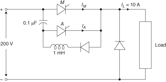
Figure 2.4 Turning off a thyristor (voltage commutation).
2.2.2 Gate Turn-Off Thyristor (GTO)
In order to avoid the use of bulky commutation circuits for turning off a thyristor, modification in the structure of the thyristor is made so that it can be turned off through gate current. This thyristor is called GTO. Similarly to thyristor, the GTO is a current-controlled minority carrier (i.e. bipolar) device. GTOs differ from conventional thyristor in that they are designed to turn off when a negative current is sent through the gate, thereby causing a reversal of the gate current. A relatively high gate current is needed to turn off the device with typical turn off gains in the range of 4–5.
It can be used in power inverter circuits as it can be switched on and off at a higher speed compared to a normal thyristor. The GTO circuit symbol is shown in Fig. 2.5. The two arrows at the gate indicate the bidirectional gate current capability. GTO is also a four-layer (p–n–p–n), three-terminal device having an anode, a cathode and gate terminals. The four layers are modelled as two transistors p–n–p and n–p–n. To turn on the GTO, a gate current is injected as in a normal thyristor. Once the device is turned on, external gate current is not necessary to keep it in on condition. To turn off a conducting GTO, the gate terminal is biased negative with respect to the cathode. However, the current required to turn off GTO is much larger than the current required for turning it on.

Figure 2.5 Gate turn-off thyristor.
2.2.3 Power Bipolar Junction Transistor
Power transistors like GTO are controlled turn-on and turn-off devices. However, a GTO requires a large reverse current through its gate to turn it off. In addition, the switching speed of GTO is very low. These disadvantages are eliminated in power transistors. They are turned on when a current signal is applied to the base or control terminal. The transistor remains in the on state so long as the control signal is present. Bipolar junction transistor (BJT) was the first power transistor developed which simplified the design of a large number of power electronic circuits that earlier used forced commutated thyristors or GTOs. Subsequently, many other devices that can broadly be classified as “Power Transistors” have been developed. Many of them have superior performance compared to the BJT in some respects. They have, by now, almost completely replaced BJTs. However, it should be emphasized that the BJT was the first semiconductor device to closely approximate an ideal fully controlled power switch. Power transistors are classified as follows:
- Bipolar junction transistors (BJTs)
- Metal–oxide–semiconductor field-effect transistors (MOSFETs)
- Insulated-gate bipolar transistors (IGBTs)
A transistor is a three-layer and three-terminal device which is either p–n–p or n–p–n with terminals marked as collector, emitter and base as shown in Fig. 2.6(a). From the point of view of construction and operation, BJT is a bipolar (i.e. minority carrier) current-controlled device. The bipolar transistors have the ability to operate within three different regions:
- Active: In this region, the transistor works as an amplifier.
- Saturation: The transistor is in the on state, offering very low forward resistance.
- Cutoff: The transistor is in the blocking state or off state.

Figure 2.6 (a) n–p–n and p–n–p transistor; (b) i-v characteristic of a bipolar transistor.
In a power electronic circuit, the power transistor is usually employed as a switch; that is, it operates in either “cutoff” (switch OFF) or saturation (switch ON) regions. However, similarly to any other switching device, it has the following limitations:
- It can conduct only a finite amount of current in the on state.
- It can have limited blocking voltage in the off state.
- It has a small forward resistance and voltage drop during “ON” condition.
- It carries a small leakage current during OFF condition.
- Can not switch on or off instantaneously.
As can be seen from its i-v characteristics in Fig. 2.6(b), a significantly large base current results in switching the device to saturation (on) state. The on-state voltage of the power transistors is about 1–2 V. BJTs are current-controlled devices, and base current must be supplied continuously to keep them in the on state. However, to turn off BJTs, simply the base current is removed.
2.2.4 Power MOSFET
A power MOSFET (Metal–Oxide–Semiconductor Field-Effect Transistor) is a voltage-controlled device and requires only a small input current to turn on. The circuit symbol of an n-channel MOSFET is shown in Fig. 2.7(a), and circuit symbol shown in Fig. 2.7(b). It has three external terminals designated as drain, source and gate. MOSFETs have very high input impedance. The current gain which is the ratio of drain current to gate current is also very high of the order of ![]() . They require low gate energy and have very fast switching speed and low switching losses.
. They require low gate energy and have very fast switching speed and low switching losses.

Figure 2.7 (a) Simplified equivalent circuit n-channel power MOSFET and (b) circuit symbol.
MOSFETs require continuous application of gate source voltage of appropriate magnitude to keep them in the on state. The MOSFET is turned off when the gate-to-source voltage is less than the threshold value which is typically 2–3 V for most of the devices. Gate current flows only during transitions from on to off or off to on conditions only. The main drawback of MOSFET is its high on-state resistance which increases with increased voltage rating. These devices are therefore more suitable for high-speed switching.
2.2.5 Insulated Gate Bipolar Transistor (IGBT)
In IGBT, the qualities of BJT and MOSFET are combined so that high switching speed of MOSFET with low conduction losses of BJT is obtained. The equivalent circuit of an n-channel IGBT is shown in Fig. 2.8(a) For p-channel IGBT, the arrow direction is reversed. The arrow basically indicates the injection of current. It also has three terminals: collector, emitter and gate. The circuit symbol of an n-channel IGBT is shown in Fig. 2.8(b). An insulated gate bipolar transistor is simply turned “ON” by applying a positive input voltage signal between the gate and the emitter, while it can be turned off by making the input gate signal zero or slightly negative with respect to the emitter. The characteristic of p-channel IGBT will be the same except that the polarities of the voltages and currents will be reversed.

Figure 2.8 (a) n-channel IGBT equivalent circuit and (b) circuit symbol.
When the gate source voltage is enough, electrons are drawn towards the gate, allowing the flow of current from source to drain. In this mode, the IGBT enters into the active region of operation, and the drain current is determined by the transfer characteristics of the device. This characteristic is qualitatively similar to that of a power MOSFET and is reasonably linear over most of the collector current range. As the gate emitter voltage is increased further, the collector current also increases, and for a given load resistance, the collector–emitter voltage decreases. When collector–emitter voltage becomes less than the gate source voltage, the IGBT enters into the saturation region. If the source gate voltage is below the threshold value, only a very small leakage current flows though the device while the collector–emitter voltage almost equals the supply voltage. In this condition, the IGBT is said to be operating in the cutoff mode.
The main advantages of using the IGBT over other types of transistor devices are its high voltage capability and low ON resistance. It has fast switching speeds compared to BJT but less than MOSFET combined with zero gate drive current, making it a good choice for moderate-speed, high-voltage applications. IGBT is most suitable for high-power applications such as the following:
- Electric vehicle motor drives
- Power factor correction converters
- Solar inverters
- Uninterruptable power supplies (UPS)
- Inductive heating cookers
2.3 ac-to-dc Converters
Wind turbines with a PM synchronous generator produce electricity at variable frequency and voltage. It therefore is first converted into dc voltage in an uncontrolled manner. The output of this converter is connected to an inverter which controls the frequency and voltage suitable for the ac system [5, 6]. The most simple ac-dc converter is single-phase uncontrolled half-wave converter which can provide a fixed output voltage. If variable voltage is required, input to this converter may be made through autotransformer. But it suffers from poor output voltage and/or input current ripple factor. The ripples can be reduced, and dc supply smoothened by connecting a capacitor at the output terminal. In addition, the input current contains a dc component which may cause problem (e.g. transformer saturation) in the power supply system. The output dc voltage is also relatively less. Some of these problems can be addressed using a full-wave rectifier described here.
2.3.1 Single-Phase Diode Bridge Rectifiers
This is one of the most popular rectifier configurations and is used widely for applications requiring dc. power output from a few hundred watts to several kilowatts. Figure 2.9(a) shows the rectifier supplying a resistive load. These rectifiers are also very widely used with capacitive loads particularly as the front end of a variable-frequency voltage source inverter.

Figure 2.9 (a) Single-phase diode bridge rectifier. (b) Resultant output waveform.
During the positive half cycle of the supply, diodes D1 and D2 are forward biased and conduct in series while diodes D3 and D4 are reverse biased. The current flows through the load as shown in Fig. 2.9. During the negative half cycle of the supply, diodes D3 and D4 are forward biased and diodes D1 and D2 are reverse biased. Now the current flows through the diodes D3 and D4 and through the load. As can be seen from Fig. 2.9, the direction of the current is the same as before. As the current flowing through the load is unidirectional, the voltage developed across the load is also unidirectional. The ripple frequency is now twice the supply frequency (e.g. 100 Hz for a 50 Hz supply or 120 Hz for a 60 Hz supply). If a smoothing capacitor C is connected, it converts the full-wave rippled output of the rectifier into a smooth dc output voltage. The output voltage with and without a capacitor is shown in Fig. 2.9(b). Generally for dc power supply circuits, the smoothing capacitor is an aluminium electrolytic type that has a capacitance value of 100 µF or more with repeated dc voltage pulses from the rectifier charging up the capacitor to peak voltage.
The main advantages of a full-wave bridge rectifier is that it has a smaller ac ripple value for a given load and a smaller smoothing capacitor compared to an equivalent half-wave rectifier. Therefore, the fundamental frequency of the ripple voltage is twice that of the ac supply, whereas for the half-wave rectifier, it is exactly equal to the supply frequency.
2.3.2 Three-Phase Full-Wave Bridge Diode Rectifiers
In large-capacity wind turbines using three-phase variable-speed generators, three-phase full-wave bridge rectifiers are used. A three-phase, six-pulse full-wave bridge diode rectifier is shown in Fig. 2.10. As shown in the figure, the anodes of three diodes are connected together in one group and the cathodes of other three diodes are connected together in another group. The three phase balances ac supply is connected as shown. The device connected to the most positive voltage will conduct in the cathode group; the other two will be reverse biased. In addition, the device connected to the most negative voltage will conduct in the anode group; the other two in this group will be reverse biased. At least two devices from positive and negative groups are simultaneously in the open state here, and at least one device from each group must conduct to facilitate the flow of the current. The voltage ripple is low because the output voltage consists of six pulses per voltage period. This circuit does not require the neutral connection of the three-phase source; therefore, a delta-connected source can also be used.

Figure 2.10 Three-phase six-pulse diode bridge rectifier.
The positive output terminal voltage is equal to the maximum of the phase voltages, and the voltage of the negative output terminal voltage is equal to the minimum of the phase voltages. In the figure, only the positive waveform of the output voltage is shown.
2.3.3 Single-Phase Fully Controlled Rectifiers
A single-phase fully controlled rectifier is shown in Figure. 2.11. It is similar to diode bridge rectifier with the difference that four diodes are replaced by four thyristors or transistors. These switches can be turned on by applying controlling pulse at any instant of time during which the anode is at a higher voltage. For R_L load and continuous load current, switches Q1 and Q4 remain in the on state beyond the positive half-wave of the source voltage Es. For this reason, the load voltage ![]() can have a negative instantaneous value. The turning on of switches Q2 and Q4 has two effects: in the case of thyristors, this will turn off Q1 and Q4 and the load current will flow through them. This type of converter is known as line-commutated converter. The output voltage is controlled by controlling the turning-on period of the switches.
can have a negative instantaneous value. The turning on of switches Q2 and Q4 has two effects: in the case of thyristors, this will turn off Q1 and Q4 and the load current will flow through them. This type of converter is known as line-commutated converter. The output voltage is controlled by controlling the turning-on period of the switches.
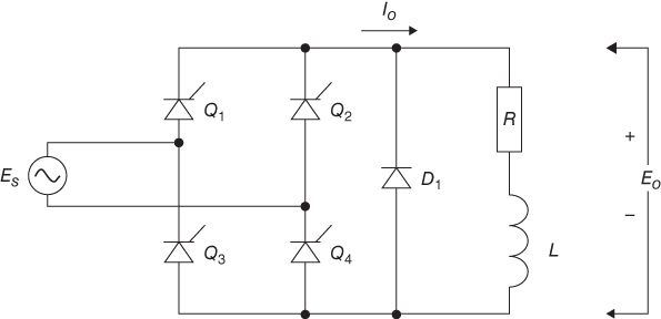
Figure 2.11 Single-phase controlled bridge rectifier.
Under normal operating condition of the converter, the load current may or may not remain zero over some interval of the input voltage cycle. If load current I0 is always greater than zero, then the converter is said to be operating in the continuous conduction mode. In the discontinuous conduction mode, none of the switches carry the current over some portion of the input cycle. The load current remains zero during that period. The disadvantage of phase-controlled converters is that for a low voltage output, their power factor is low.
2.3.4 Three-Phase Fully Controlled Bridge Converter
In three-phase fully controlled bridge converter, the diodes as shown in Fig. 2.10 are replaced by thyristors (transistor) as shown in Fig. 2.12. This circuit is also known as a three-phase full-wave bridge or as a six-pulse converter. The thyristors are triggered at an interval of π/6 radians (i.e. at an interval of 30°). The frequency of the output ripple voltage is 6 fs.

Figure 2.12 Three-phase controlled bridge rectifier.
Three-phase converters are used when large power is to be controlled. Control over the output dc voltage is obtained by controlling the conduction interval of each thyristor. This method is known as phase control, and the converters are also called “phase-controlled converters”.
The three-phase bridge rectifiers have following advantages:
- Low ripple
- High power factor
- Simple construction
2.4 dc-to-ac Converters (Inverters)
In renewable energy systems, power electronic interface is required to convert dc power generated by PV solar system or fuel cell into ac power which may be directly used in isolated systems [7, 8] or for connection to grids. When connected to a power grid, these are used to inject sinusoidal current into the power system with required THD and high power factor. The inverters available for power conversion are as follows:
- Single-phase and three-phase voltage source inverters
- Single-phase and three-phase current source inverters
2.4.1 Single-Phase Voltage Source Inverters
Figure 2.13 shows the power circuit diagram for single-phase voltage source H-bridge inverter. In this, four switches (in two legs) are used to generate the ac waveform at the output. Any semiconductor switch such as GTO, IGBT, MOSFET or BJT can be used. For inductive load, the stored energy is fed back through diodes connected across the switches. These diodes are called as Feedback Diodes.
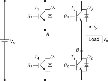
Figure 2.13 Single-phase voltage source bridge inverter.
Anti-parallel diodes are not required for resistive load because load current io is in phase with output voltage vo.
2.4.2 Square-Wave PWM Inverter
In full-wave bridge inverter, shown in Fig. 2.13, there are two arms of the bridge with two switches in each arm. The switches in each branch are operated alternatively so that they are not in the same mode (ON/OFF) simultaneously. When ![]() are on and
are on and ![]() and
and ![]() are off, the output voltage across the load is Vs, and when
are off, the output voltage across the load is Vs, and when ![]() and
and ![]() conduct, the output voltage is –Vs. The switches
conduct, the output voltage is –Vs. The switches ![]() and
and ![]() conduct for a period of 0 < t ≤ T/2, and the switches
conduct for a period of 0 < t ≤ T/2, and the switches ![]() and
and ![]() conduct for a period of T/2 < t ≤ T, where T is the time period of the conduction of switches. The frequency of output ac voltage is given by 1/T. The frequency can be varied by varying the T or conduction period of the switch with the help of the gate (base) signal. The root mean square (rms) value of the output ac voltage is
conduct for a period of T/2 < t ≤ T, where T is the time period of the conduction of switches. The frequency of output ac voltage is given by 1/T. The frequency can be varied by varying the T or conduction period of the switch with the help of the gate (base) signal. The root mean square (rms) value of the output ac voltage is

The following PWM techniques are used for controlling the output ac rms voltage and frequency control in an inverter.
- Single-pulse-width modulation
- Multiple-pulse-width modulation
- Sinusoidal-pulse-width modulation
2.4.3 Single-Pulse-Width Modulation
In single-pulse-width modulation control, there is only one pulse per half cycle and the output rms voltage is changed by varying the width of the pulse. The gating signals for the switches are generated by comparing a rectangular reference signal of amplitude Vc with a triangular reference carrier signal Vcar. The time period of the two signals is nearly equal. The gating signals and output voltages of single-pulse-width modulation are shown in Fig 2.14(a) and (b). The frequency of the control signal determines the frequency of the output voltage. The instantaneous output voltage is ![]() corresponding to
corresponding to ![]() and
and ![]() conducting and equal to
conducting and equal to ![]() corresponding to
corresponding to ![]() and
and ![]() conducting. If δ is the time period for which
conducting. If δ is the time period for which ![]() and
and ![]() conduct and also
conduct and also ![]() and
and ![]() , then the rms value of output voltage is
, then the rms value of output voltage is


Figure 2.14 (a) Gating signal for single-pulse-width modulated single-phase inverter. (b) Output voltage.
By varying ![]() from 0 to Vcar, the pulse width δ can be varied from 0 to π, and the rms output voltage from 0 to
from 0 to Vcar, the pulse width δ can be varied from 0 to π, and the rms output voltage from 0 to ![]() .
.
The output voltage consists of a rectangular pulse in each half cycle which can be expressed as

2.4.4 Multiple-Pulse-Width Modulation
In this modulation, there are multiple numbers of output pulses per half cycle, and all pulses are of equal width. The gating signals are generated by comparing a rectangular reference with a triangular reference. The frequency of the reference signal ![]() determines the number of pulses per half cycle m, whereas the frequency of reference signal
determines the number of pulses per half cycle m, whereas the frequency of reference signal ![]() sets the output frequency f. The modulation index controls the output voltage. This type of modulation is also known as symmetrical pulse-width modulation. The number of pulses
sets the output frequency f. The modulation index controls the output voltage. This type of modulation is also known as symmetrical pulse-width modulation. The number of pulses ![]() per half cycle is found from the expression
per half cycle is found from the expression  .
.
2.4.5 Sinusoidal-Pulse-Width Modulation
In sinusoidal pulse-width modulation, there are multiple pulses per half-cycle as described earlier, but the width of each pulse is varied over the output cycle, in a sinusoidal manner. The scheme, in its simplified form, involves comparison of a high-frequency triangular carrier voltage with a sinusoidal modulating signal that represents the desired fundamental frequency component of the voltage waveform. The peak magnitude of the modulating signal is limited to the peak magnitude of the carrier signal. The comparator output is then used to control the high-side and low-side switches. The two types of pulse-width modulation inverters are bipolar and unipolar switching. Each unique switching technique creates either a unipolar or a bipolar output at the load. Figure 2.15 shows the gating signals and output voltage of SPWM with unipolar switching. In this scheme, the switches in the two legs of the full-bridge inverter are not switched simultaneously, as in the bipolar scheme. In this unipolar scheme, the legs A and B of the full-bridge inverter are controlled separately by comparing the carrier triangular wave vcar with the control sinusoidal signals vc and –vc, respectively. This SPWM is generally used in industrial applications. The number of pulses per half cycle depends upon the ratio of the frequency of the carrier signal (fc) to the modulating sinusoidal signal. The frequency of the control signal or the modulating signal sets the inverter output frequency (fo) and the peak magnitude of the control signal controls the modulation index ma which in turn controls the rms output voltage. If ton is the width of nth pulse, the rms output voltage can be determined by


Figure 2.15 (a) Gating signal and (b) output voltage for sinusoidal PWM of single phase.
The amplitude modulation index is defined as

where,
| = | peak magnitude of the control signal (modulating sine wave) | |
| = | peak magnitude of peak magnitude of the carrier signal (triangular signal). |
The frequency modulation ratio is defined as

2.4.6 Three-Phase Voltage Source Inverters
Figure 2.16 shows a three-phase voltage source inverter circuit. The inverter is fed by a dc voltage and has three phase legs, each consisting of two transistors and two diodes (labelled) with subscripts (a, b, c). A common inverter control method is sine–triangle pulse-width modulation (STPWM) control. With STPWM control, the switches of the inverter are controlled based on a comparison of a sinusoidal control signal and a triangular switching signal. There are three sinusoidal reference waves, each displaced by 120°. A triangular carrier wave is compared with the reference signal of each phase to generate a control signal for that phase.

Figure 2.16 Three-phase voltage source inverter.
The sinusoidal control waveform establishes the desired fundamental frequency of the inverter output, while the triangular waveform establishes the switching frequency of the inverter. The ratio between the frequencies of the triangle wave and the sinusoid is referred to as the modulation frequency ratio.
The sinusoidal PWM control signal generation is shown in Fig. 2.17(a). In theory, the switches in each leg are never both on or off simultaneously; therefore, the voltages ![]() ,
, ![]() and
and ![]() fluctuate between the input voltage (Vdc) and zero. By controlling the switches in this manner, the output voltages are ac, with the fundamental frequency corresponding to the frequency of the sinusoidal control voltage as shown in Fig. 2.17(b). In most instances, the magnitude of the triangle wave is held fixed. The amplitude of the inverter output voltages is therefore controlled by adjusting the amplitude of the sinusoidal control voltages. The ratio of the amplitude of the sinusoidal waveforms relative to the amplitude of the triangle wave is the amplitude modulation index similarly to a single-phase inverter. The diodes provide paths for current when a transistor is turned on but cannot conduct the polarity of the load current. For example, if the load current is negative at the instant, the upper transistor is gated on, the diode in parallel with the upper transistor will conduct until the load current becomes positive at which time the upper transistor will begin to conduct.
fluctuate between the input voltage (Vdc) and zero. By controlling the switches in this manner, the output voltages are ac, with the fundamental frequency corresponding to the frequency of the sinusoidal control voltage as shown in Fig. 2.17(b). In most instances, the magnitude of the triangle wave is held fixed. The amplitude of the inverter output voltages is therefore controlled by adjusting the amplitude of the sinusoidal control voltages. The ratio of the amplitude of the sinusoidal waveforms relative to the amplitude of the triangle wave is the amplitude modulation index similarly to a single-phase inverter. The diodes provide paths for current when a transistor is turned on but cannot conduct the polarity of the load current. For example, if the load current is negative at the instant, the upper transistor is gated on, the diode in parallel with the upper transistor will conduct until the load current becomes positive at which time the upper transistor will begin to conduct.

Figure 2.17 (a) Generation of control signal for sinusoidal PWM three-phase inverter. (b) Output voltage waveform.
2.4.7 Single-Phase Current Source Inverters
The voltage source inverters are fed from a voltage source, and the load current alternates from positive to negative value. In a current source inverter, the output current is maintained constant irrespective of the load, and the voltage is changed between positive and negative values. A single-phase current source inverter with transistor switches is shown in Fig. 2.18. The output of this inverter is near-square-wave current. In CSI, no feedback diodes are required, and the switching devices must withstand peak reverse voltages. The transistors conduct in the sequence ![]() ;
; ![]() ;
; ![]() ;
; ![]() , and so on.
, and so on.
Figure 2.18 Single-phase current source inverter.
The load current can be expressed as

2.4.7.1 Three-Phase Current Source Inverter
The circuit of a three-phase current source inverter (CSI) is shown in Fig. 2.19. As in single-phase CSI, the three–phase inverter is also operated from a current source. There are six switches, two in each arm as in the case of voltage source inverters. There is a 60° phase displacement between commutation of the upper device followed by commutation of the lower device.

Figure 2.19 Three-phase current source inverter.
If thyristors are used as switches then, six diodes, each one in series with the respective thyristor, are needed here, as used for single-phase CSI. Six capacitors, three each in two (top and bottom) halves, are used for commutation. If transistors are used instead of thyristors, capacitors for commutation are not required.
For three-phase current source inverter and star-connected load, the output current in Fourier series can be written as

2.5 Multilevel Inverters
Multilevel converters have been developed to provide high power with medium-voltage semiconductor switches. Multilevel inverters achieve higher power by using a series of power semiconductor switches along with several lower voltage dc sources to perform the power conversion by synthesizing a staircase voltage waveform. The term multilevel was used initially for the three-level converter. Subsequently, several multilevel converter topologies have been developed. To achieve a three-level waveform, a single full-bridge inverter is employed. Basically, a full-bridge inverter is known as an H-bridge cell. This inverter produces three output voltage levels, +V, –V and 0. In order to produce high power and high voltage, multilevel inverters are used in which the number of voltage levels is increased. As the number of voltage level increases, the harmonic contents of the output voltage decreases. Multilevel inverters are widely utilized in industrial field employing motor drives, static VAR compensators and renewable energy systems and so on.
The general structure of a multilevel inverter is to synthesize a near-sinusoidal waveform from several levels of dc voltages. The capacitor voltages can be added by connecting them in series with the help of power electronic switches to provide multilevel of voltages. In this way, a high voltage is reached at the output, while the power semiconductor devices withstand only reduced voltages.
The most attractive features of multilevel inverters are as follows [9–11].
They can generate output voltages with extremely low distortion and lower ![]() .
.
- 1. They draw input current with very low distortion.
- 2. They generate smaller common-mode (CM) voltages.
- 3. They can operate with a lower switching frequency.
There are three types of multilevel inverters in use. These are as follows:
- Diode-clamped multilevel inverter
- Flying-capacitor multilevel inverter
- Cascaded multicell inverter
2.5.1 Diode-Clamped Multilevel Inverter
The diode-clamped inverter provides multiple voltage levels through connection of the phases to a series bank of capacitors. It typically consists of (m − 1) capacitors on the dc bus and produces m levels of phase voltage. A three-level diode-clamped inverter is shown in Fig. 2.20(a). In this circuit, the dc bus voltage is split into three levels by two series-connected bulk capacitors, ![]() and
and ![]() . The middle point of the two capacitors n can be defined as the neutral point. It is therefore also known as neutral-point clamped multilevel inverter. The output voltage
. The middle point of the two capacitors n can be defined as the neutral point. It is therefore also known as neutral-point clamped multilevel inverter. The output voltage ![]() is ac and has three states:
is ac and has three states: ![]() , 0 and
, 0 and ![]() . To obtain the voltage level of
. To obtain the voltage level of ![]() , switches
, switches ![]() and
and ![]() need to be turned on; for
need to be turned on; for ![]() , switches
, switches ![]() and
and ![]() need to be turned on; and for the 0 level,
need to be turned on; and for the 0 level, ![]() and
and ![]() need to be turned on.
need to be turned on.

Figure 2.20 (a) A three-level diode-clamped inverter. (b) A five-level diode-clamped inverter.
The key components that distinguish this circuit from a conventional two-level inverter are two diodes ![]() and
and ![]() . These two diodes clamp the switch voltage to half the level of the dc bus voltage. If the output is taken between a and 0, then the circuit becomes a dc/dc converter, which has three output voltage levels:
. These two diodes clamp the switch voltage to half the level of the dc bus voltage. If the output is taken between a and 0, then the circuit becomes a dc/dc converter, which has three output voltage levels: ![]() ,
, ![]() and 0. It is the most commonly used topology in the industry for a number of levels equal to 3.
and 0. It is the most commonly used topology in the industry for a number of levels equal to 3.
Figure 2.20(b) shows a five-level diode-clamped converter in which the dc bus consists of four capacitors, ![]() ,
, ![]() ,
, ![]() and
and ![]() . For input voltage
. For input voltage ![]() , the voltage across each capacitor is
, the voltage across each capacitor is ![]() , and each device will be stressed to one capacitor voltage level through clamping diodes. The staircase voltage is synthesized through five switch combinations of five voltage levels across a and n. The five voltage levels are
, and each device will be stressed to one capacitor voltage level through clamping diodes. The staircase voltage is synthesized through five switch combinations of five voltage levels across a and n. The five voltage levels are ![]() ,
, ![]() , 0,
, 0, ![]() and
and ![]() .
.
2.5.2 Flying-Capacitor Multilevel Inverter
Flying-capacitor inverter is quite similar to diode-clamped multilevel inverter. This type of multilevel inverter requires the capacitor to be pre-charged to a varying voltage level. By changing the switching states, the capacitors and dc source are connected in different connection configurations and produce various line-to-ground output voltages. Figure 2.21 illustrates the fundamental building block of a phase-leg capacitor-clamped inverter. The circuit is also called the flying-capacitor inverter with independent capacitors clamping the device voltage to one capacitor voltage level. The inverter in Fig. 2.21(a) provides a three-level output across a and n, ![]() , which is
, which is ![]() , 0 and
, 0 and ![]() . Every cell has a single capacitor and two power switches. Power switch is a combination of a transistor connected with an anti-parallel diode. The switching of devices is similar to the one used for diode-clamped inverter.
. Every cell has a single capacitor and two power switches. Power switch is a combination of a transistor connected with an anti-parallel diode. The switching of devices is similar to the one used for diode-clamped inverter.

Figure 2.21 (a) Three-level capacitor-clamped inverter; (b) five-level.
Five-level capacitor-clamped inverter is shown in Fig. 2.21(b). The voltage synthesis in a five-level capacitor-clamped converter has more flexibility compared to a diode-clamped converter. The voltage of the five-level phase leg a output with respect to the neutral point n can be synthesized with many combinations of switch positions. As the number of levels is increased, many capacitors are required which makes this topology heavy and cumbersome. Since large numbers of capacitors are required, it can provide storage capability during power outages.
2.5.3 Cascaded Multicell with Different dc Source Inverter
Cascaded multicell inverter is based on the series connection of single-phase inverters with separate dc sources. A cascaded multicell inverter (CMCI) differs in several ways from diode-clamped MLI and CCMLI in the manner in which the multilevel voltage waveform is obtained. It uses cascaded full-bridge inverters with separate dc sources, in a modular setup, to create the stepped waveform. Figure 2.22 shows the power circuit of one phase leg of a nine-level cascaded multicell inverter with four cells in each phase. It basically consists of a series of H-bridge inverter units. The resulting phase voltage is synthesized by the addition of the voltages generated by the different cells, each supplied by a different dc source. Each single-phase full-bridge inverter generates three voltages at the output: ![]() , 0 and
, 0 and ![]() . This is made possible by connecting the capacitors sequentially to the ac side via the four power switches. The resulting output ac voltage swings from 4 to −4 with nine levels, and the staircase waveform is nearly sinusoidal, even without filtering.
. This is made possible by connecting the capacitors sequentially to the ac side via the four power switches. The resulting output ac voltage swings from 4 to −4 with nine levels, and the staircase waveform is nearly sinusoidal, even without filtering.

Figure 2.22 (a) Cascaded inverter circuit; (b) waveforms.
2.6 Resonant Converters
In the PWM and other inverters described earlier, the switches are operated in the switch mode where they are subjected to full load current during each switching. Thus, these switches are subjected to high switching stresses and losses. They are also responsible for electromagnetic interference (EMI). Normally, a higher switching frequency of operation of power converters is desirable, as it allows the size of inductors and capacitors to be reduced, leading to cheaper and more compact circuits. However, with a higher switching frequency, the losses and also EMI are increased.
Resonant power converters contain resonant L-C circuits whose voltage and current waveforms have sinusoidal variations during one or more subintervals of each switching period. Since a sinusoidal waveform is produced, the current and voltage pass through zero at each half cycle. The switches can be turned on or off when either the current though them or the voltage across them is zero.
The following types of resonant converters topologies are commonly used.
- Series resonant converters
- Parallel resonant converters
- Series–parallel resonant converters
- Zero-voltage switching (ZVS) resonant converters
- Zero-current switching (ZCS) resonant converters
- Resonant dc-link inverters
2.6.1 Series Resonant Converter
In series resonant converters (SRCs), the resonating circuit and the switching device are connected in series with the load to form an underdamped circuit. These circuits are based on resonant current oscillations. The series resonant inverters can be implemented by employing either unidirectional or bidirectional switches. The unidirectional switch can be a thyristor, GTO, bipolar transistor, IGBT and so on. In a bidirectional switch, an anti-parallel diode connected with the switching device or RCT (reverse-conducting thyristor) can be used. The circuit diagram of a full-bridge SRC with bidirectional switches is shown in Fig. 2.23. One method of controlling the output voltage in resonant converters is to control the switching frequency of the full-bridge inverter. This method is called “variable frequency control”.

Figure 2.23 Series resonant converter.
There are three possible modes of operation depending on whether switching frequency ![]() is more than, less than or equal to resonance frequency
is more than, less than or equal to resonance frequency ![]() . There are no switching loss d in the switches at
. There are no switching loss d in the switches at ![]() since the load current will be passing through zero exactly at the time when the switches change state. However, when
since the load current will be passing through zero exactly at the time when the switches change state. However, when ![]() or
or ![]() , the switches are subjected to losses. For instance, if
, the switches are subjected to losses. For instance, if ![]() the load current will flow through the switch at the beginning of each half cycle and then commutate to the diode when the current changes polarity. These transitions are lossless. However, when the switch turns on or when the diode turns off, they are subjected to simultaneous step changes in voltage and current. These transitions therefore produce losses. As a result, each of the four devices is subjected to only one lossy transition per cycle.
the load current will flow through the switch at the beginning of each half cycle and then commutate to the diode when the current changes polarity. These transitions are lossless. However, when the switch turns on or when the diode turns off, they are subjected to simultaneous step changes in voltage and current. These transitions therefore produce losses. As a result, each of the four devices is subjected to only one lossy transition per cycle.
2.6.1.1 Discontinuous Conduction Mode
In this mode, the resonant current is interrupted in every cycle. This control mode theoretically avoids switching losses because whenever a switch turns on or off, its current is zero. The shortcoming of this control mode is the distorted current waveform which may not be suitable for many applications including PV system.
2.6.2 Parallel Resonant Inverter
A parallel resonant inverter is supplied from a current source. This circuit offers higher impedance to switch current. Since here the current is continuously controlled, it has better short-circuit response. It is used in low-power applications. The circuit is shown in Fig. 2.24.

Figure 2.24 Parallel resonant converter.
2.6.3 ZCS Resonant Converters
The switches in a zero-current resonant switch converter are turned on and off at zero current. A step-down dc-dc converter using the ZCS configuration is shown in Fig. 2.25. Prior to turning the switch on, the output current freewheels through the diode, both the current ![]() in L and the voltage
in L and the voltage ![]() across C are zero. After turning the switch on, the diode conducts and the total input voltage develops across L, the current
across C are zero. After turning the switch on, the diode conducts and the total input voltage develops across L, the current ![]() rises linearly, ensuring ZCS and soft current change. When i reaches
rises linearly, ensuring ZCS and soft current change. When i reaches ![]() , the current conduction stops in diode
, the current conduction stops in diode ![]() . At this time, the L-C resonant circuit starts resonating and the change in
. At this time, the L-C resonant circuit starts resonating and the change in ![]() and
and ![]() will be sinusoidal. The peak current
will be sinusoidal. The peak current ![]() where
where ![]() is
is ![]() and peak voltage
and peak voltage ![]() at
at ![]() must be larger than I
must be larger than I ![]() ; otherwise,
; otherwise, ![]() will not swing back to zero. When the current
will not swing back to zero. When the current ![]() becomes zero, the switch is turned off automatically. Now the capacitor supplies the load current and therefore its voltage falls linearly till it becomes zero. The load current during this time freewheels through the diode. Now the switch can be turned on after this time, and the cycle is repeated. The output voltage will be equal to the average value of voltage
becomes zero, the switch is turned off automatically. Now the capacitor supplies the load current and therefore its voltage falls linearly till it becomes zero. The load current during this time freewheels through the diode. Now the switch can be turned on after this time, and the cycle is repeated. The output voltage will be equal to the average value of voltage ![]() which can be varied by changing the switching frequency.
which can be varied by changing the switching frequency.

Figure 2.25 ZCS resonant converter.
2.6.4 ZVS Resonant Converter
The switches of ZVS resonant converter are turned on and off at zero voltage. The capacitor of ZVS is connected in parallel with the switch as shown in Fig. 2.26. Initially, the switch and the diode ![]() are off, and the capacitor charges at a constant rate of load current I. When the capacitor is fully charged, the current becomes zero and then starts to flow through diode
are off, and the capacitor charges at a constant rate of load current I. When the capacitor is fully charged, the current becomes zero and then starts to flow through diode ![]() because of inductance in the circuit. The capacitor voltage reaches a peak value and then starts decreasing till it is equal to the source voltage. After this, the capacitor voltage continues to fall till it becomes zero. Now the switchs is turned on at zero voltage. The diode will still be conducting till the current through the inductor equals the load current. At this time, the diode stops conducting and the load current conducts through the switch till it is turned off again.
because of inductance in the circuit. The capacitor voltage reaches a peak value and then starts decreasing till it is equal to the source voltage. After this, the capacitor voltage continues to fall till it becomes zero. Now the switchs is turned on at zero voltage. The diode will still be conducting till the current through the inductor equals the load current. At this time, the diode stops conducting and the load current conducts through the switch till it is turned off again.

Figure 2.26 ZVS resonant converter.
2.6.5 Resonant dc-Link Inverters
In a resonant dc-link inverter, a simple LC resonant circuit is placed between the dc bus and a PWM inverter. A three-phase resonant dc-link inverter is shown in Fig. 2.27. The six switches ![]() are switched in such a manner that it sets up periodic oscillations in the dc-link LC circuit. The switches are turned on and off at zero link voltages to reduce the losses. The turning on of the switch as zero voltage is no problem as the device is turned on when its anti-parallel diode is conducting, presenting zero voltage.
are switched in such a manner that it sets up periodic oscillations in the dc-link LC circuit. The switches are turned on and off at zero link voltages to reduce the losses. The turning on of the switch as zero voltage is no problem as the device is turned on when its anti-parallel diode is conducting, presenting zero voltage.
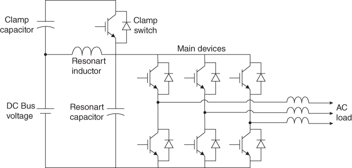
Figure 2.27 Resonant dc-link inverter.
The dc-link resonant cycle is normally started with a fixed value of the initial capacitor current. This may result in the voltage across the dc link to be more than twice the input voltage. This voltage will appear across the switches which may require high rating devices. An active clamp shown in Fig. 2.27 is connected to limited link voltage.
2.7 Matrix Converters
The matrix converter is a direct frequency converter, which can perform ac/ac, dc/ac and dc/dc conversions [12–14]. It is single-stage converter which has an array (matrix) of ![]() bidirectional switches connecting m-phase voltage source to n-phase load. It uses bidirectional switches, with a switch connected between each input terminal and each output terminal as shown in Fig. 2.28. The matrix converter shown in Fig. 2.28 is a
bidirectional switches connecting m-phase voltage source to n-phase load. It uses bidirectional switches, with a switch connected between each input terminal and each output terminal as shown in Fig. 2.28. The matrix converter shown in Fig. 2.28 is a ![]() matrix converter which consists of nine bidirectional switches that allow any output phase to be connected to any input phase. A
matrix converter which consists of nine bidirectional switches that allow any output phase to be connected to any input phase. A ![]() matrix has 27 possible switching states. The source voltage and load voltage are related by the following equation:
matrix has 27 possible switching states. The source voltage and load voltage are related by the following equation:


Figure 2.28 Matrix converter.
Equation (2.9) gives the instantaneous relationship between the input and output voltages. The switches can have a value of either 0 or 1, depending on whether they are off or on. The operating conditions of this type of converter demands that the input phases of the converter should never be short-circuited and the output currents should not be interrupted. Basically, this means that one and only one bidirectional switch per output phase must be switched on at any instant.
Since no energy storage components are present between the input and output sides of the matrix converter, the output voltages have to be generated directly from the input voltages. Each output voltage waveform is synthesized by sequential piece-wise sampling of the input voltage waveforms. The sampling rate has to be set much higher than both input and output frequencies, and the duration of each sample is controlled in such a way that the average value of the output waveform within each sample period tracks the desired output waveform. The maximum output voltage the matrix converter can generate without entering the over-modulation range is equal to ![]() of the maximum input voltage; this is an intrinsic limit of the matrix converter, and it holds for any method of control.
of the maximum input voltage; this is an intrinsic limit of the matrix converter, and it holds for any method of control.
The control methods for a matrix converter are quite complex and will not be discussed here.
2.8 Summary
All the renewable energy systems require specific power electronic converters to convert the power generated into useful power that can be directly interconnected with the utility grid and/or can be used for specific consumer applications locally. In this chapter, power electronic converters to convert ac to dc, dc to ac, dc to dc and ac-dc-ac conversion are presented. First, various types of power electronic devices that can be used as switches are discussed. Finally, the converter topologies which are suitable for wind, solar and energy storage are discussed.
References
- 1 Baliga, B.J. (1987) Modern Power Electronic Devices, Wiley.
- 2 Rashid, M.H. (2004) Power Electronic Circuits Devices and Applications, 3rd edn, Pearson.
- 3 Ahmad, M. (1996) Industrial Drives, Chapter 10, Macmillan, India.
- 4 Bacha, S. et al. (2014) Power Electronic Converters Modeling and Control with Case Studies, Springer Verlag, London.
- 5 Erickson, R.W. (1997) Fundamental of Power Electronics, Springer Science.
- 6 Mohan, N. et al. (2002) Power Electronics: Converters, Applications, and Design, 3rd edn, Wiley.
- 7 Blaabjerg, F. et al. (2004) Power electronics as efficient interface in dispersed power generation systems. IEEE Transactions on Power Electronics, 19 (5), 1184–1194.
- 8 Kramer W et al. (2008) Advanced Power Electronic Interfaces for Distributed Energy Systems Technical Report NREL
- 9 Rodriguez, J. et al. (2002) Multilevel inverters: a survey of topologies, controls, and applications. IEEE Transactions on Industrial Electronics, 49 (4), 724–738.
- 10 Lai, J.S. and Peng, F.Z. (1996) Multilevel converters-a new breed of power converters. IEEE Transactions on Industry Applications, 32 (3), 509–517.
- 11 Mei, J. et al. (2013) Modular multilevel inverter with new modulation method and its application to photovoltaic grid connected generator. IEEE Transactions on Power Electronics, 28 (11), 5063–5073.
- 12 Wheeler, P. et al. (2002) Matrix converters: a technology review. IEEE Transactions on Power Electronics, 49 (2), 276–288.
- 13 Empringham, L. et al. (2013) Technological issues and industrial application of matrix converters: a review. IEEE Transactions on Industrial Electronics, 60 (10), 4260–4271.
- 14 Wheeler, P.W. et al. (2002) Matrix converters: a technology review. IEEE Transaction Industrial Electronics, 49 (2), 276–288.