
15
The 12 series 8 pin microcontroller
Arizona Microchip have a range of microcontrollers with 8 pins. They include types with Data EEPROM and A/D converters. In this section we will cover the 12C508 and 12C509, which are one time programmable devices and the flash 12F629 and 12F675 (electronically) reprogrammable devices.
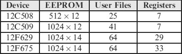
The device memory specifications are shown in Table 15.1.
Table 15.1 12C508/509, 12F629 and 12F675 memory specifications
Features of these 12 series
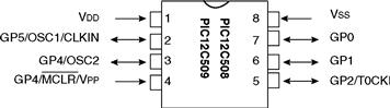
One of the special features of this Micro is that it has 8 pins, but 6 of them can be used as I/O pins, the remaining 2 pins being used for the power supply. There is no need to add a crystal and capacitors, because a 4MHz oscillator is built on board! If you wish to use a clock other than the 4MHz provided, then you can connect an oscillator circuit to pins 2 and 3 (as in the 16F84). That leaves you with of course only 4 I/O.
Being an 8 pin device means of course it is smaller than an 18 pin device and cheaper. The on board oscillator means that the crystal and timing capacitors are not required, reducing the component count, size and cost even further. So if your application requires no more than 6 I/O these are devices to use. They have useful applications in burglar alarm circuits and the radio transmitter circuits we have looked at previously.
The memory maps of the 12C508 and 12F629/675
The memory map of the 12C508 is shown in Figure 15.3, showing the 7 registers and 25 user files. Figure 15.4 shows the 12F629/675 map.
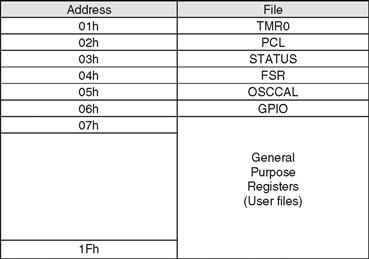
Figure 15.3 12C508 Memory map
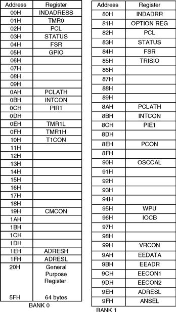
Figure 15.4 12F629/675 Memory map
The 12C509 has 16 extra user files mapped in Bank1.
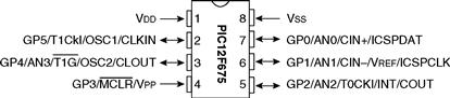
There is no longer a PORTA or PORTB because we only have 6 I/O, they are in a port called GPIO (General Purpose Input Output), File 6.
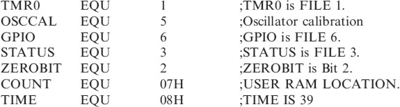
Oscillator calibration
Apart from the small size of this device an appealing feature is that the oscillator is on board. The file OSCCAL is an oscillator calibration file used to trim the 4MHz oscillator.
The 4MHz oscillator takes its timing from an on board R-C network, which is not very precise. So these chips have a value that can be put into OSCCAL to trim it. This value is stored in the last memory address i.e. 01FFh for the 12C508 and 03FFh for the 12C509 and 12F629/675.
The code, which is loaded by the manufacturer in the last memory location for the 12C508/9, is MOVLW XX where XX is the trimming value. The last memory location is the reset vector i.e. when switched on the micro goes to this location first, it loads the calibration value into W and the program counter overflows to 000h and continues executing the code. To use the calibration value, in the Configuration Section write the instruction MOVWF OSCCAL, which then moves the manufacturers calibration value into the timing circuit.
There is one point to remember – if you are using a windowed device then the calibration value will be erased when the memory is erased. So make a note of the MOVLW XX code by looking in MPLAB with: VIEW-PROGRAM MEMORY and program it back in by ORG 01FFH MOVLW XX.
A calibration instruction is programmed into the last location of program memory, i.e. 3FFH. The instruction is RETLW XX, where XX is the calibration value. This value is placed in the OSCCAL register to set the calibration value of the internal oscillator. This is done in the 12F629 header as
| CALL | 3FFH | ;call instruction at location 3FFH |
| MOVWF | OSCCAL | ;move calibration value to OSCCAL |
The trimming can be ignored if required – but it only requires 1 or 2 lines of code, so why not use it.
I/O PORT, GPIO
The GPIO, General Purpose Input/Output, is an 8 bit I/O register, it has 6 I/O lines available so bits GPIO 0 to 5 are used, bits 6 and 7 are not.
N.B. GPIO bit3 is an input only pin so there is a maximum of 5 outputs.
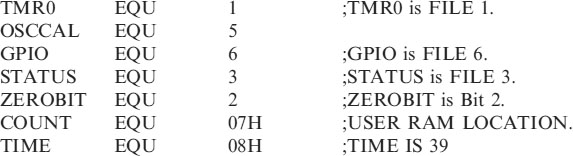
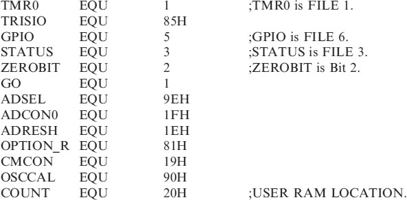
• For the 12C508 GPIO pins 0,1 and 3 can be configured with weak pull ups by writing 0 to OPTION,6 (bit 6 in the OPTION register).
• For the 12F629/675 all GPIO pins except GPIO3 can be configured with weak pull ups. This is done by setting the relevant bits in the Weak Pull Up Register, WPU. When in
| Bank1 | MOVLW | B′00110111′ |
| MOVWF | WPU |
Will turn on all the weak pull ups.
![]()
Figure 15.5 Weak pull up register
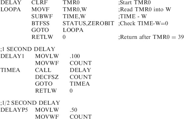
Delays with the 12 series
We have previously used a 32kHz. Crystal with the 16F84 device, but now we are going to use the internal 4MHz clock.
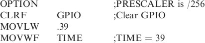
A 4MHz clock means that the basic timing is ¼ of this i.e. 1MHz. If we set the OPTION register to divide by 256 this gives a timing frequency of 3906Hz. In the headers for the 12C508/9, 12F629 and 12F675 I have (as with the 16F84) included a one second and a 0.5 second delay. In order to achieve a one second delay from a frequency of 3906Hz I first of all produced a delay of 1/100 second by counting 39 timing pulses i.e. 3906Hz/39 = 100.15 = 100Hz approx., called DELAY. A one second delay, subroutine DELAY1 then counts 100 of these DELAY times (i.e. 100 × 1/100 second), and of course a delay of 0.5 seconds would count 50.
Just before we look at the headers – we do not have an instruction SUBLW on the 12C508. I have therefore set up a file called TIME that I have written 39 into. I then move TMR0 into W and subtract the file TIME (39d) from it to see if TMR0 = 39 i.e. 1/100 of a second has elapsed.
WARNING: The 12C508 and 509 micros only have a two level deep stack. Which means when you do e.g. a one second delay, CALL DELAY1 this then calls another subroutine, i.e. CALL DELAY. You have used your two levels and cannot do any further calls without returning from one at least one of those subroutines. If you did make a third CALL the program would not be able to find its way back!
Header for 12C508/9
;HEAD12C508.ASM FOR 12C508/9.
;**********************************************************
| LIST | P=12C508 | ;We are using the 12C508. |
| ORG | 0 | ;0 is the start address. |
| GOTO | START | ;goto start! |
;**********************************************************
| __CONFIG H′0FEA′ | ;selects internal RC oscillator, WDT off, |
| ;code protection disabled |
;************************************************************
;SUBROUTINE SECTION.

;**********************************************************
; CONFIGURATION SECTION.

;**********************************************************
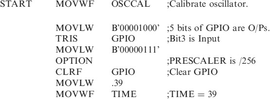
Program application for 12C508
There are 5 I/O on the 12C508 i.e. GPIO bits 0,1,2,4 and 5. Bit3 is an input only. For our application we will chase 5 LEDs on our outputs backwards and forwards at 0.5 second intervals.
The Circuit diagram is shown in Figure 15.6.
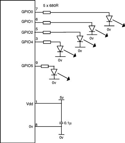
Figure 15.6 LED chasing circuit for the 12C508
Notice that the only other component required is the power supply decoupling capacitor, 0.1µF, no oscillator circuit is required.
The program for the LED Chasing Project, LED_CH12.ASM is shown below.
;LED_CH12.ASM Program to chase 5 LEDs with the 12C508
;**********************************************************
| LIST | P=12C508 | ;We are using the 12C508. |
| ORG | 0 | ;0 is the start address. |
| GOTO | START | ;goto start! |
;**********************************************************
| _CONFIG H′0FEA′ | ;selects Internal RC oscillator, WDT off, |
| ;Code Protection disabled. |
;**********************************************************
;SUBROUTINE SECTION.

;**********************************************************
;**********************************************************
;Program starts now.
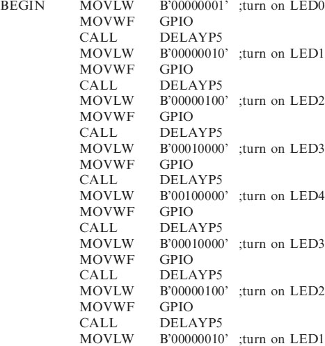

The program is similar in content to the 16F84 programs used previously, but with the following exceptions:
• A file TIME, file 8, has been set up which has had 39 loaded into it, in the Configuration Section. This is used to determine when TMR0 has reached a count of 39, time of 0.01 seconds, which is then used in the timing subroutines.
• In the Configuration Section the first instruction the program encounters is MOVWF OSCCAL. This moves the calibration value which has just been read by MOVLW XX, from location 1FFH, the first instruction, into the calibration file OSCCAL.
• GPIO is used in the program instead of the usual PORTA and PORTB.
Program application using the 12F629/675
To perform the LED chasing action of the previous example in Figure 15.6 using the 12F675 the following code would be required.
;LED_CH675.ASM FOR 12F675 using 4MHz internal RC.
;**********************************************************
| LIST | P=12F675 | ;We are using the 12F675. |
| ORG | 0 | ;0 is the start address. |
| GOTO | START | ;goto start! |
;***************************************************
| __CONFIG H′3F84′ | ;selects Internal RC oscillator, WDT off, |
| ;Code Protection disabled. |
;**********************************************************
;SUBROUTINE SECTION.
;*******************************************************
;CONFIGURATION SECTION.
;**********************************************************
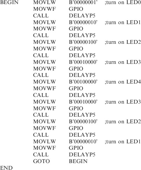
The differences in the code between the 12C508 and 12F675 are:
![]()
These two lines are used to inform the 12F675 that the inputs are all digital. Change the data to make the inputs analogue – refer to manufacturers data. These two lines are not required for the 12F629 which does not have any A/D.
![]()
These lines are used to calibrate the internal 4MHz oscillator.
![]()
The 12F629/675 have analogue comparators, which we have not looked at. They need to be turned off to use the I/O pins. The default is that the comparators are on!
There are numerous other 12 series microcontrollers but once you have understood how to move from the 12C508/9 to the 12F629/675 you will be able to migrate to the rest.