
6
Understanding the headers
The 16F84
HEADER84.ASM The header for the 16F84.
Now that we have looked at a number of applications we are ready to understand HEADER84.ASM introduced in Chapter 2.
• The header starts with a title that includes the name of the file, this is useful when you are printing it out and details about what the program is doing.
| ;HEADER84.ASM for 16F84. | This sets PORTA as an INPUT (NB 1 |
| ; | means input) and PORTB as an OUTPUT |
| ; | (NB 0 means output). The OPTION |
| ; | register is set to /256 to give timing pulses |
| ; | of 1/32 of a second. |
| ; | 1second and 0.5 second delays are |
| ; | included in the subroutine section. |
;*********************************************************
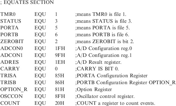
• The EQUATES section tells the software what numbers your words represent. When you write your program you use mnemonics such as PORTA, PORTB, TMR0, STATUS, ZEROBIT, COUNT, MYAGE. The Assembler Program does not understand your words; it is looking for the file number or the bit number. You have to tell it what these mean in the Equates Section i.e. COUNT is File 0C, PortA is file 5, the STATUS register is file 3, ZEROBIT is bit 2, etc. The memory map of the 16F84 in Table 6.1 shows the addresses of the registers and user files. The file with address 0C is the first of the user files and I have called it COUNT, it stores the number of times certain events have happened in my program.
Table 6.1 16F84 memory map
| FILE ADDRESS | FILE NAME | FILE NAME |
| 00 | INDIRECT | INDIRECT |
| ADDRESS | ADDRESS | |
| 01 | TMR0 | OPTION |
| 02 | PCL | PCL |
| 03 | STATUS | STATUS |
| 04 | FST | FSR |
| 05 | PORTA | TRISA |
| 06 | PORTB | TRISB |
| 07 | – | – |
| 08 | EEDATA | EECON1 |
| 09 | EDADR | EECON2 |
| 0A | PCLATH | PCLATH |
| 0B | INTCON | INTCON |
| 0C | 68 | |
| USER | ||
| 4F | FILES | |
| BANK0 | BANK1 |
I could have file 0D as COUNT2, file 0E as COUNT3, file 0F as SECONDS or WAIT etc.

| LIST | P=16F84 | ;we are using the 16F84. |
| ORG | 0 | ;the start address in memory is 0 |
| GOTO | START | ;goto start! |
LIST P=16F84 tells the assembler what chip to assemble the code for. ORG 0 means put the next line of code into program memory address 0, then follow with next line in address1 etc.
GOTO START makes the program bypass the subroutine section and GOTO the label START which is where the device is configured before executing the body of the program. The instruction GOTO START is placed in EPROM address 0 by ORG 0.
The line DELAY1 CLRF TMR0 is then placed in program memory address 1, etc.
To avoid having to set the configuration bits when we come to program the device they can be set in the code. You can change these bits if you require in MPLAB, note the new number and substitute it in the code.
; Configuration Bits
| __CONFIG H′3FF0′ | ;selects LP oscillator, WDT off, PUT on, |
| ;Code Protection disabled. |
The subroutine section consists of 2 subroutines DELAY1 and DELAYP5.
A subroutine is a section of program, which is, used a number of times instead of rewriting it and using up program memory. Just call it i.e. CALL DELAY1, at the end you RETURN to the program in the position you left it. The stack is the register that remembers where you came from and returns you back.
The DELAY1 code is:

DELAY1 starts by clearing the register TMR0 (timer 0), with CLRF TMR0, i.e. CleaR the File TMR0. This sets the timer to zero and will be counting TMR0 pulses every 1/32 of a second.
LOOPA MOVF TMR0,W is move file TMR0 into the working register, W.
We want to know when TMR0 is 32, because then we will have had 32 TIMER0 pulses, which is 1 second. This is done with a subtraction as in the example earlier in this Chapter 5, in the section on the hot air blower.
The label LOOPA is there because we keep returning to it until TMR0 reaches the required value.
There is no instruction, which asks the micro is TMR0 equal to 32. So we have to use the instructions available. We subtract a number from W and ask is the answer 0. If for example we subtract 135 from W and the answer is 0 then W contained 135 if the answer was not 0 then W did not contain 135. The status register contains a bit called a zerobit, it is bit2. Notice in the EQUATES section I have put ZEROBIT EQU 2. So I can use ZEROBIT in my code instead of 2 − I would soon forget what the 2 was supposed to mean. The zerobit is set to a 1 when the result of a previous calculation is 0. So a 1 means result was 0!!!! Think of this as a flag (because that's what it is called), the flag is waving (a 1) to indicated the result is zero. We can test this zerobit, i.e. look at it and see if it is a 1 or 0. We can skip the next instruction if it is set, (a zero has occurred), by BTFSS STATUS, ZEROBIT or skip if clear, (a zero has not occurred), by BTFSC STATUS, ZEROBIT. Doesn't this read better than BTFSC 3,2 STATUS is Register3, ZEROBIT is bit 2.
Lets look at this subroutine again.
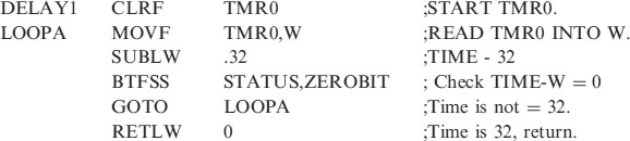
• Then move TMR0 into W (MOVF TMR0,W)
• SUBTRACT 32 from W which now holds TMR0 value. (SUBLW .32)
• If W (hence TMR0) is 32 the zerobit is set, we skip the next instruction and return from the subroutine with 0 in W (RETLW 0)
• If W is not 32 then we do not skip and we GOTO LOOPA and put TMR0 in W and repeat until TMR0 is 32.
DELAYP5 is a similar code but TMR0 now is only allowed to count upto 16 i.e. a half-second (with 32 pulses a second). Note if you copy and paste, change the name of the subroutine from DELAY1 to DELAYP5, change the 32 to 16 and do not forget to change LOOPA to LOOPB. You cannot goto room 27 if there are two room 27s!
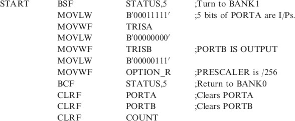
The instruction BSF STATUS,5 sets bit 5 in the Status Register. As you can see from the explanation of the Status Register bits in Chapter 19, bit 5 is a page select bit which selects page 1 giving us access to the Registers in the page 1 (Bank1) column of the memory map in Table 6.1. The reason for pages or banks is that we have an 8 bit micro. 8 bits can only address 256 files so to identify a file we have it on a page, like a line in a book i.e. line 17 on page 40 instead of line 2475.
| MOVLW | B′00011111′ | ;5bits of PORTB are I/P |
| MOVWF | TRISA |
These 2 lines move 11111 into the data direction register to set the 5 bits of PORTA as inputs. The 11111 is first moved to W (MOVLW B’00011111’) and then into the data direction register with MOVWF TRISA. A 1 signifies an input a 0 an output.
| MOVLW | B′00000000′ | ;8bits of PORTB are O/P |
| MOVWF | TRISB |
These 2 lines move 00000000 into the data direction register to set the 8 bits of PORTB as outputs. The 000000 is first moved to W and then into the data direction register with MOVWF TRISB.
PortA and PortB can be configured differently if required. E.g. to make the lower 4 bits of PortB outputs and the upper 4 bits inputs - alter the 2 lines of the program with:
| MOVLW | B′11110000′ |
| MOVWF | TRISB |
The header also sets the internal clock to divide by 256 i.e. a 32.768kHz clock gives a program execution of 32.768 kHz/4 = 8.192 kHz. If the prescaler is set to divide by 256 this gives timing pulses of 32 a second.
The prescaler is configured with the 2 lines:
| MOVLW | B′00000111′ | ;Prescaler is /256 |
| MOVWF | OPTION_R | ;TIMER is 1/32 sec. |
The OPTION register can be altered in the header to give faster timing pulses if required, as described in the OPTION Register section in Chapter 19.
| The line | BCF STATUS,5 | ;Return to Bank0. |
then returns to page 0 on the memory map. The good news here is in the programs in this book we only need to go into page 1 in the Configuration Section. The body of the program, your section, resides in page 0.
We then finish the configuration section by clearing any outputs in PORTA and PORTB with,
| CLRF | PORTA | ;Clears PortA. |
| CLRF | PORTB | ;Clears PortB. |
This will not affect any bits that are configured as inputs.
Just for good measure the COUNT file is also cleared with CLRF COUNT.
16F84 memory map
The Memory Map of the 16F84 is shown in Table 6.1.
This diagram shows the position of the Special Function Registers, i.e. PORTA, PORTB, TMR0 etc. in addresses 00 to 0B and the location of the User Files i.e. COUNT (the only one we have used up to now) occupying locations 0C through to 4F.
These files are very important when writing our code. The Special Function Registers enable us to tell the microcontroller to do things, i.e. set PORTB up as an output port with TRISB, alter the rate of TMR0 with the OPTION register, find out if the result of a calculation is zero, +ve or −ve using the STATUS register. TMR0 of course tells us how much time has elapsed.
The other microcontroller which features frequently in this book, my favourite, is the 16F818. We will look at its header and memory map now and compare it to the 16F84 to see how they differ. After that you will be able to distinguish between other micros.
The 16F818
HEAD818.ASM The header for the 16F818.
The code shown below is the header for the 16F818 that we first saw in Chapter 4.
;HEAD818.ASM for 16F818. This sets PORTA as digital INPUT.
;PORTB is an OUTPUT.
;Internal oscillator of 31.25kHz chosen
;The OPTION register is set to /256 giving timing pulses of 32.768 ms.
;1second and 0.5 second delays are included in the subroutine section.
;*********************************************************
;*********************************************************
| LIST | P= 16F818 | ;we are using the 16F818. |
| ORG | 0 | ;the start address in memory is 0 |
| GOTO | START | ;goto start! |
;*********************************************************
| __CONFIG H′3F10′ | ;sets INTRC-A6 is port I/O, WDT off, PUT |
| ;on, MCLR tied to VDD A5 is I/O | |
| ;BOD off, LVP disabled, EE protect disabled, | |
| ;Flash Program Write disabled, | |
| ;Background Debugger Mode disabled, CCP | |
| ;function on B2, | |
| ;Code Protection disabled. |
;*****************************************************
;SUBROUTINE SECTION.

;*********************************************************
;CONFIGURATION SECTION.

;*********************************************************
END
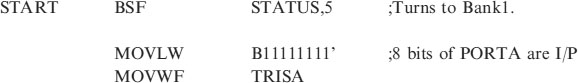
We will now consider only the new additions to the previous HEADER84. ASM for the 16F84.
• PORTA is now an 8 I/O port, NB. PORTA,5 is input only.
• ADCON0, ADCON1 and ADRES are Special Function Registers that will enable us to instruct the microcontroller on how we want the A/D converter to function. We will discuss these when we consider A/D conversion in Chapter 11.
• OSCCON allows us to set the value of the internal oscillator. We can choose from 8MHz, 4MHz, 2MHz, 1MHz, 500kHz, 250kHz, 125kHz or 31.25 kHz. The use of OSCCON is described in the Register section in Chapter 19.
• CONFIGURATION BITS. There are more functions on the 16F818 than the 16F84 so there are more choices in the way it is configured. Here we have selected the internal oscillator so we do not need the crystal, that has freed up 2 I/O lines. The master clear, MCLR has been switched internally to Vdd (5v) freeing up another I/O line, giving 16 I/O. We have switched the brown out off this would reset the micro if the supply voltage fell below a critical point avoiding erratic behaviour. Low voltage programming has been switched off. EEPROM protection and Program Write Protection has been disabled. Background Debugger Mode has been disabled. The 16F818 is capable of working with the Microchip In Circuit Debugger (ICD2). Capture and Compare Pulse Width Module (CCP) not discussed in this book has been switched onto B2.
• SUBROUTINE SECTION.The 16F818 header described uses the internal 31.25kHz oscillator, which does not lend itself so easily to times of seconds. I have had to write a different code for the delays. A 31.25kHz clock gives timing pulses of 32µs which do not add up exactly to give a second. The delay loop similar in its action to the 16F84 delay has had 2 NOP (no operation) instructions added to make up the shortfall. The 0.1 second delay is therefore 0.099968s which is as close as I could get it. If you really need accurate times you will need to use a crystal for your timing. The internal oscillators are only about 1% accurate.
• CONFIGURATION SECTION.Because the 16F818 has an A/D converter on board you need to tell it which PORTA inputs are analogue and which are digital. Analogue inputs are dealt with in Chapter 11 for now PORTA has been set to all digital inputs with:
| MOVLW | B′00000110′ | ;PORTA IS DIGITAL |
| MOVWF | ADCON1 |
The internal oscillator is set to 31.25kHz with:
| MOVLW | B′00000000′ | |
| MOVWF | OSCCON | ;oscillator 31.25kHz |
This is a default condition and is therefore not required. I have included it incase you are wondering how the frequency is set. You need to alter the data in OSCCON to change the frequency, see Chapter 19.Because the 16F818 has more functions than the 16F84 it follows that there are more Special Function Registers to handle these extra functions. It also has more user files.
These files are now arranged over 4 banks, BANK0, BANK1, BANK2 and BANK3. The Banks are selected by the Bank Select bits (page select bits) in the Status Register, RP0 and RP1, bits 5 and 6, shown in Figure 6.1.
![]()
Figure 6.1 Status register bits
| So | 00 selects Bank0 |
| 01 selects Bank1 | |
| 10 selects Bank2 | |
| 11 selects Bank3 |
For most applications in this book once we have configured the device we will not need to change banks. The only time we do change is when we look at applications involving the Data EEPROM.
The 16F818 memory Map is shown below in Figure 6.2.

Figure 6.2 16F818 memory map
We will now continue with some more applications and introduce some more instructions and ideas. Each of these programs will be able to be executed using a number of micros using the appropriate headers.