
16
The 16F87X microcontroller
The 16F87X range includes the devices, 16F870, 16F871, 16F872, 16F873, 16F874, 16F876 and 16F877. They are basically the same device but differ in the amounts of I/O, analogue inputs, program memory, data memory (RAM) and EEPROM data memory that they have.
The 16F87X have more I/O, program memory, data memory, EEPROM data memory and analogue inputs than the 16F818.

16F87X memory map
The 16F87X devices have more functions than we have seen previously. These functions of course need registers in order to make the various selections.
The memory map of the 16F87X showing these registers is shown in Figure 16.3.

Figure 16.1 The 16F870/2/3/6 pinout

Figure 16.2 The 16F87X data sheet

Figure 16.3 The 16F87X memory map
The 16F87X devices have a number of extra registers that are not required in the applications we have looked at. For an explanation of these registers please see Microchip's website @ www.microchip.com, where you can download the data sheet as a pdf (portable document file), which can be read using Adobe Acrobat Reader.
The 16F872 microcontroller
In order to demonstrate the operation of the 16F87X series we will consider the 16F872 device. This is a 28pin device with 22 I/O available on 3 ports. PortA has 6 I/O, PortB has 8 I/O and PORTC has 8 I/O. Of the 6 I/O available on PortA 5 of them can be analogue inputs. The header for the 16F872, HEAD872.ASM, configures the device with 5 analogue inputs on PortA, 8 digital inputs on PortC and 8 outputs on PortB. The port configuration for the device is shown in Figure 16.4.

Figure 16.4 Port configuration of the 16F872
The 16F872 has been configured in HEAD872.ASM, using a 32 kHz crystal, to allow all the programs used previously to be copied over with as little alteration as possible.
The 16F872 header
HEAD872.ASM
;EQUATES SECTION
| TMR0 | EQU | 1 |
| OPTION_R | EQU | 1 |
| PORTA | EQU | 5 |
| PORTB | EQU | 6 |
| PORTC | EQU | 7 |
| TRISA | EQU | 5 |
| TRISB | EQU | 6 |
| TRISC | EQU | 7 |
| STATUS | EQU | 3 |
| ZEROBIT | EQU | 2 |
| CARRY | EQU | 0 |
| EEADR | EQU | 0DH |
| EEDATA | EQU | 0CH |
| EECON1 | EQU | 0CH |
| EECON2 | EQU | 0DH |
| RD | EQU | 0 |
| WR | EQU | 1 |
| WREN | EQU | 2 |
| ADCON0 | EQU | 1FH |
| ADCON1 | EQU | 1FH |
| ADRES | EQU | 1EH |
| CHS0 | EQU | 3 |
| GODONE | EQU | 2 |
| COUNT | EQU | 20H |
;*****************************************************
| LIST | P=16F872 |
| ORG | 0 |
| GOTO | START |
;*******************************************************

;******************************************************************
;CONFIGURATION SECTION.


;*********************************************************
;Program starts now.
Explanation of HEAD872.ASM
Equates Section
• We have a third port, PORTC file 7 and its corresponding TRIS file, TRISC file 7 on Bank1. The TRIS file sets the I/O direction of the port bits.
• The EEPROM data file addresses have been included. EEADR is file 0Dh in Bank2, EEDATA is file 0Ch in Bank2, EECON is file 0Ch in Bank3 and EECON2 is file 0Dh in Bank3.
• The EEPROM data bits have been added. RD the read bit is bit 0, WR the write bit is bit 1, WREN the write enable bit is bit 2.
• The Analogue files ADRES, ADCON1 and ADCON2 have been included as have the associated bits CHS0 channel 0 select bit 3 and the GODONE bit, bit 2.
List Section
• This of course indicates the microcontroller being used, the 16F872 and that the first memory location is 0. In address 0 is the instruction GOTO START that instructs the micro to bypass the subroutine section and goto the configuration section at the label START.
Subroutine Section
Configuration Section
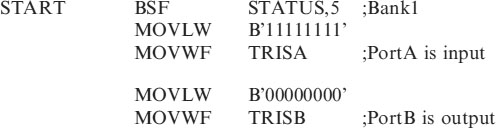
• As before we need to switch to Bank1 to address the TRIS files to configure the I/O. PORTA is set as an input port with the two instructions
| MOVLW | B′00000111′ |
| MOVWF | TRISA |
PORTB and PORTC are configured in a similar manner using TRISB and TRISC.
• The Option register is configured with the instructions
| MOVLW | B′00000111′ |
| MOVWF | OPTION_R |
• The A/D register is configured with the instructions
| MOVLW | B′00000000′ |
| MOVWF | ADCON1 |
Setting PORTA bits 0, 1, 2, 3 and 5 as analogue inputs.
• We turn to Bank3 by setting Bank select bit, STATUS,6 (bit 5 is still set) so that we can address EECON1, the EEPROM data control register. BSF EECON1 then enables access to the EEPROM program memory when required.
• We then turn back to Bank0 by clearing bits 5 and 6 of the Status register and clear the files PortA, PortB and PortC.
16F872 Application – a greenhouse control
In order to demonstrate the operation of the 16F872 and to develop our programming skills a little further consider the following application.
• A greenhouse has its temperature monitored so that a heater is turned on when the temperature drops below 15°C and turns the heater off when the temperature is above 17°C.
• A probe in the soil monitors the soil moisture so that a water valve will open for 5 seconds to irrigate the soil if it dries out. The valve is closed and will not be active for a further 5 seconds to give the water time to drain into the soil.
• A float switch monitors the level of the water and sounds an alarm if the water drops below a minimum level.
The circuit diagram for the greenhouse control is shown in Figure 16.5 and the flowchart is drawn in Figure 16.6.

Figure 16.5 Greenhouse control circuit
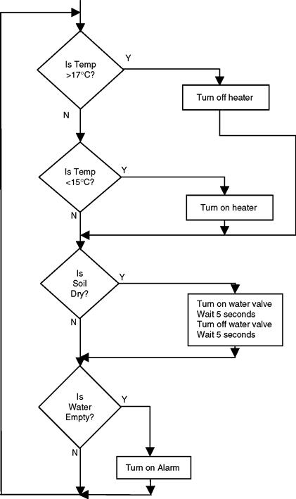
Figure 16.6 Greenhouse control flowchart
Greenhouse program
In order to program the analogue/digital settings consider the NTC Thermister. As the temperature increases the resistance of the thermister will decrease and so the voltage presented to AN0 will increase.
Let us assume the voltage is 2.9v at 15°C and 3.2v at 17°C they correspond to digital readings of 2.9 × 51 = 147.9 i.e. 148 and 3.2 × 51 = 163.2 i.e. 163. (N.B. 5v = 255, so 1v = 51 we are using an 8 bit A/D.)
Our program then needs to check when AN0 goes above 163 and below 148.
As the soil dries out its resistance will increase. Let us assume in our application dry soil will give a reading of 2.6v, (on AN1), i.e. 2.6 × 51 = 132.6 i.e. 133. So any reading above 133 is considered dry.
The float switch is a digital input showing 1 if the water level is above the minimum required and a 0 if it is below the minimum.
Greenhouse code
The code for the greenhouse uses HEAD872.ASM with the program instuctions added and saved as GREENHO.ASM.
;EQUATES SECTION
| TMR0 | EQU | 1 |
| OPTION_R | EQU | 1 |
| PORTA | EQU | 5 |
| PORTB | EQU | 6 |
| PORTC | EQU | 7 |
| TRISA | EQU | 5 |
| TRISB | EQU | 6 |
| TRISC | EQU | 7 |
| STATUS | EQU | 3 |
| ZEROBIT | EQU | 2 |
| CARRY | EQU | 0 |
| EEADR | EQU | 0DH |
| EEDATA | EQU | 0CH |
| EECON1 | EQU | 0CH |
| EECON2 | EQU | 0DH |
| RD | EQU | 0 |
| WR | EQU | 1 |
| WREN | EQU | 2 |
| ADCON0 | EQU | 1FH |
| ADCON1 | EQU | 1FH |
| ADRES | EQU | 1EH |
| CHS0 | EQU | 3 |
| GODONE | EQU | 2 |
| COUNT | EQU | 20H |
;*****************************************************
| LIST | P=16F872 |
| ORG | 0 |
| GOTO | START |
;*******************************************************
;Configuration Bits
| __CONFIG H′3F30′ | ;selects LP oscillator, WDT off, PUT on, |
| ;Code Protection disabled. |
;*******************************************************
;SUBROUTINE SECTION.

;******************************************************************

;*********************************************************


Explanation of code
In the previous analogue circuits in Chapter 11 we only used 1 analogue input on AN0. We now have two analogue inputs on AN0 and AN1. When making an analogue measurement we must specify which analogue channel we wish to measure. The default is AN0 when moving to AN1 we select AN1 by setting channel select bit0 i.e. BSF ADCON0, CHS0.
When moving back to AN0 clear the channel select bit. The 8 channels, AN0 to AN7 are seclected using bits, CHS2, CHS1, CHS0.
• The temperature is read on AN0 with and then checked to see if it is greater than 17°C, by subtracting the A/D reading from 163 (the reading equating to 17°C). The carry bit in the status register indicates if the result is +ve or −ve being set or clear. We then go to turn off the heater if the temperature is above 17°C or check if the temperature is below 15°C. In which case we turn on the heater.
• The soil moisture is checked next. AN1 is selected and the reading compared this time to 133 indicating dry soil. The program either goes to turn on the water valve if the soil is dry or continues to check the water level if the soil is wet.
• If the water level is below minimum then the alarm sounds, if above minimum the alarm is turned off. The program then repeats the checking of the inputs and reacts to them accordingly.
Programming the 16F872 microcontroller using PICSTART PLUS
Once the pogram GREENHO.ASM has been saved it is then assembled using MPASMWIN. The next step as previously is to program GREENHO.HEX into the micro using PICSTART PLUS.
This process has been outlined in Chapter 2, but there are a few more selections to attend to in the ‘Device Specification’ Section.
• Select the device 16F872, if this device is not available you will require a later version of MPLAB, obtainable from www.microchip.com.
Configuration bits
The configuration bit settings when programming the 16F872 for the Greenhouse program are shown in Figure 16.7.

Figure 16.7 Greenhouse program configuration bits
Reconfiguring the 16F872 header
• The port settings are changed as they were for the 16F84 i.e. a 1 means the pin is an input and a 0 means an output.
• The Option Register is configured as in the 16F84 see also Chapter 19.
• The A/D convertor configuration is adjusted using A/D configuration register 1, i.e. ADCON1 shown in Figure 16.8.
![]()
Figure 16.8 ADCON1, A/D port configuration register 1
Bit7 is the A/D Format Select bit, which selects which bits of the A/D result registers are used. I.e. the A/D can use 10 bits which requires two result registers, ADRESH and ADRESL. Two formats are available.
(a) the most significant bits of ADRESH read as 0, with ADFM = 1
![]()
Or (b) the least significant bits of ADRESL read as 0, with ADFM = 0
![]()
For 8 bit operation condition (b) is used with ADRESH as the 8 most significant bits of the A/D result. This is the default configuration used in HEADER872.ASM where ADRESH (ADRES in the equates) is register 1Eh in Bank0.
Table 16.1 shows the A/D Port Configuration settings for PCFG3, PCFG2, PCFG1 and PCFG0.
Table 16.1 A/D Port configuration

A = Analogue Input, D = Digital input.
Vdd = +ve supply, Vss = −ve supply.
Vref+ = high voltage reference.
Vref− = low voltage reference.
A3 = PortA,3 A2 = PortA,2 etc.
N.B. AN7, AN6 and AN5 are only available on the 40 pin devices 16F871, 16F874 and 16F877.