
18
Projects
Project 1 Electronic dice
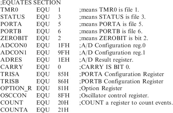
When using a Microcontroller in a control system the place to start is to decide what hardware you are controlling. In the Electronic Dice we will use 7 LEDs for the display and a push button to make the “throw”. Just to make the dice a little more interesting we will use a buzzer to give an audible indication of the number thrown.
The circuit for the Dice is shown in Figure 18.1, using the 16F818 with its internal 31.25kHz clock. The push button is an input connected to PortA,2. The 7 LEDs are connected to PortB and the buzzer is on A1.

Figure 18.1 Circuit diagram for the electronic dice
The truth table for the dice is shown in Table 18.1.
Table 18.1 Truth table for the electronic dice

How does it work?
The dice has an input – the “throw” button. When it is pressed the internal count repeatedly runs through from 1 to 6 changing some 8000 times a second and stops on a number when the button is released.
This would be a complicated circuit to design with a timer, counter and decoder circuits. But now we can use one chip to do all the timing counting and decoding functions. Not only that I have also added a light flashing routine for the first few seconds when the dice is turned on. Try doing all that with one chip – other than a microcontroller.
The best way to describe the action of a program is with a flowchart. The flowchart for the dice is shown in Figure 18.2.
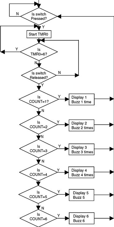
Figure 18.2 Flowchart for the dice
Program listing for the dice
The full program listing for the dice is given below in; DICE.ASM.
;*********************************************************
| LIST | P=16F818 | ;we are using the 16F818. |
| ORG | 0 | ;the start address in memory is 0 |
| GOTO | START | ;goto start! |
;*********************************************************
;Configuration Bits
| __CONFIG H′3F10′ | ;sets INTRC-A6 is port I/O, WDT off, PUT on, |
| ;MCLR tied to VDD A5 is I/O | |
| ;BOD off, LVP disabled, EE protect disabled, | |
| ;Flash Program Write disabled, | |
| ;Background Debugger Mode disabled, CCP | |
| ;function on B2, | |
| ;Code Protection disabled. |
;**********************************************************
;SUBROUTINE SECTION.


;**********************************************************

;**********************************************************
;Program starts now.
Modifications to the dice project
Can you think of any modifications you can make to this program? Perhaps you could add a roll routine so that a few numbers are shown before the dice finally comes to rest on the number.
The initial display routine could also be customized.
You could throw a 7.
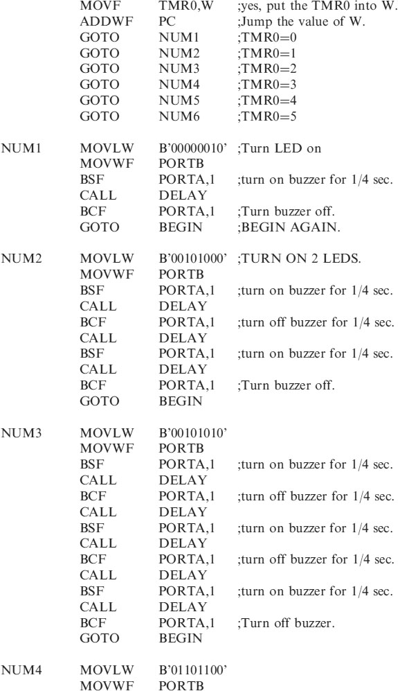
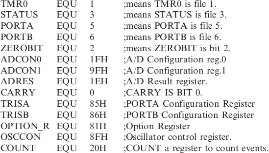
Project 2 Reaction timer
There are many question and answer games on the market that would benefit from a reaction timer which indicates the first player of a team to press. This project has the facility for up to 6 players.
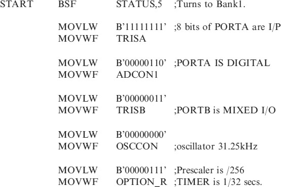
The circuit diagram for this project illustrated in Figure 18.3 uses 6 inputs and 7 outputs.
Figure 18.3 The reaction timer circuit
Reaction timer operation
If B0 is the first to press B6 output LED lights
If B1 is the first to press B7 output LED lights
If B2 is the first to press A0 output LED lights
If B3 is the first to press A1 output LED lights
If B4 is the first to press A2 output LED lights
If B5 is the first to press A3 output LED lights
The Buzzer is connected to A4.
The buzzer sounds for 4 seconds after a button is pressed. During this time no further presses are acknowledged. After the 4 seconds the buzzer stops and the LED is extinguished and the program resets.
The unit uses 13 I/O but not all 6 button/LED combinations need be used. The program will not need altering.
Just one point in case you were wondering: B0–B5 have been used as inputs instead of PORTA because PORTB has internal pull-up resistors on the inputs. The switches do not need their own – no point in using 5 resistors if you don't have to.
The reaction timer program
;*********************************************************
| LIST | P=16F818 | ;we are using the 16F818. |
| ORG | 0 | ;the start address in memory is 0 |
| GOTO | START | ;goto start! |
;*********************************************************
| __CONFIG H′3F10′ | ;sets INTRC-A6 is port I/O, WDT off, PUT on, |
| ;MCLR tied to VDD A5 is I/O | |
| ;BOD off, LVP disabled, EE protect disabled, | |
| ;Flash Program Write disabled, | |
| ;Background Debugger Mode disabled, CCP | |
| ;function on B2, | |
| ;Code Protection disabled. |
;*****************************************************
;SUBROUTINE SECTION.

;**********************************************************
;**********************************************************
;Program starts now.


How does it work?
The program starts by turning all the LEDs and the buzzer on for 1 second to check they are all working.
The program then tests each input in turn starting with B0, if it is set i.e. not pressed the program skips and checks the next input. When the last input B5 is checked and it is not pressed then the program skips the next instruction and goes back to SCAN again.
If one of the inputs is pressed the program branches to the relevant subroutine to turn on the appropriate LED and buzzer for 4 seconds before returning to scan the switches again.
Reaction timer development
One way of making this program more interesting and to develop your programming skills – when a button is pressed have the outputs jump around B6, A0, A3, A1, A2 then B7 before landing on the correct output.
You could also have a flashing light routine at the start of the program to check they are working, you could also pulse the buzzer. The buzzer could be made to beep a number of times to give an audible indication of who was first to press. Another modification you could make is – think of one yourself, I'm not doing all the work.
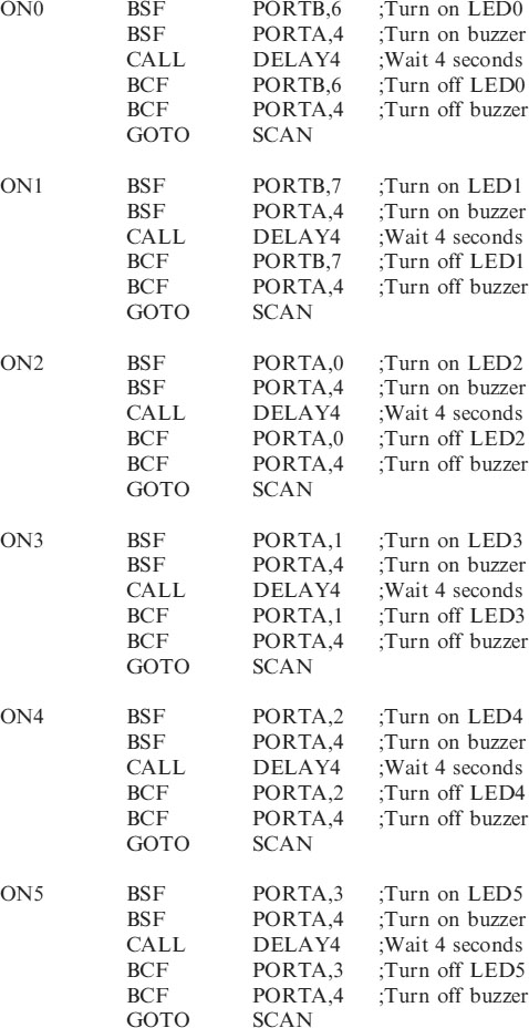
Project 3 Burglar alarm
Operation
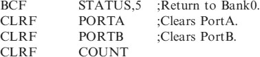
The circuit for the Burglar Alarm is shown in Figure 18.4 using the 16F818.
Figure 18.4 Burglar alarm circuit
It uses two inputs, SW0 and SW1 which are both normally closed. They can represent Door contacts, Passive Infra red sensor outputs, window contacts or tilt switches.
SW0 has a delay on it but SW1 is immediately active.
Both switches can have additional switches wired in series with them to provide extra security cover. If SW1 is a window contact in a caravan it could have a tilt switch wired in series with it, so if the caravan was moved the siren would sound immediately.
SW0 and SW1 are connected to PORTB so pull-ups are not required.
A buzzer is used to indicate entry and exit delays on the alarm and a siren is connected to the micro via an IRF511 (Power MOSFET).
How does it work?
Consider the flow chart in Figure 18.5.

Figure 18.5 Burglar alarm flowchart
With reference to the flow chart:
When the alarm is switched on a 30 second exit delay is activated and the buzzer sounds for this time.
Switches 0 and 1 are continually checked until one of them is open.
If SW0 is opened a 30 second entry delay is activated and the buzzer sounds for this time, the siren will then sound for 5 minutes.
If SW1 is opened the siren will sound immediately for 5 minutes.
The switches are then checked until they are both closed when the alarm resets back to checking switches 0 and 1 until one of them opens again.
Switching off the power would disable the alarm.
Burglar alarm project code
The code for the Burglar Alarm is shown below in ALARM.ASM
;*********************************************************
| LIST | P=16F818 | ;we are using the 16F818. |
| ORG | 0 | ;the start address in memory is 0 |
| GOTO | START | ;goto start! |
;*********************************************************
;Configuration Bits
| __CONFIG H′3F10′ | ;sets INTRC-A6 is port I/O, WDT off, PUT on, |
| ;MCLR tied to VDD A5 is I/O | |
| ;BOD off, LVP disabled, EE protect disabled, | |
| ;Flash Program Write disabled, | |
| ;Background Debugger Mode disabled, | |
| ;CCP function on B2, | |
| ;Code Protection disabled. |
;**********************************************************


;**********************************************************
;**********************************************************

The Burglar Alarm uses 2 inputs and 2 outputs a total of 4 I/O.
We can therefore program the Alarm with a 12C508 chip.
Burglar alarm using the 12C508
The circuit diagram for the Alarm with the 12C508 is shown in Figure 18.6.

Figure 18.6 Burglar alarm using 12C508
Note in the circuit of Figure 18.6, showing the alarm using the 12C508, that no external oscillator circuit is required and that pull ups are not required on pins GPIO,0 or GPIO,1 (or GPIO,3). N.B. GPIO,3 is an input only pin.
The flowchart of course is the same. The code is shown below as ALARM_12.ASM using the header for the 12C508 from Chapter 15.
WARNING: The 12C508 only has a two level deep stack which means when you do a CALL you can only do one more CALL from that subroutine otherwise the program will get lost.
Program code for 12C508 burglar alarm
;ALARM_12.ASM FOR 12C508

;**********************************************************
| LIST | P=12C508 | ;We are using the 12C508. |
| ORG | 0 | ;0 is the start address. |
| GOTO | START | ;goto start! |
;**********************************************************
| __CONFIG H′0FEA′ | ;selects Internal RC oscillator, WDT off, |
| ;Code Protection disabled. |
;**********************************************************
;SUBROUTINE SECTION.

;**********************************************************

;**********************************************************
;Program starts now.

Fault finding
What if it all goes wrong!
The block diagram of the microcontroller in Figure 18.7 shows 3 sections:

Figure 18.7 Block diagram of the microcontroller circuit
Inputs, the microcontroller and outputs.
The microcontroller makes the output respond to changes in the inputs under program control.
All microcontroller circuits will have outputs and most will have inputs.
Check the supply voltage
Check that the correct voltages are going to the pins. 5v on Vdd, pin 14 and MCLR, pin 4 and 0v on Vss, pin 5, on the 16F84.
Checking inputs
If the inputs are not providing the correct signals to the micro then the outputs will not respond correctly.
Before checking inputs or outputs it is best to remove the microcontroller from the circuit – with the power switched off. You have inserted the micro in an IC holder so that it can be removed easily! This is essential for development work.
In order to check the inputs and outputs to the microcontroller let us consider a circuit we have looked at before in Chapter 5, the Switch Scanning Circuit, shown below in Figure 18.8.
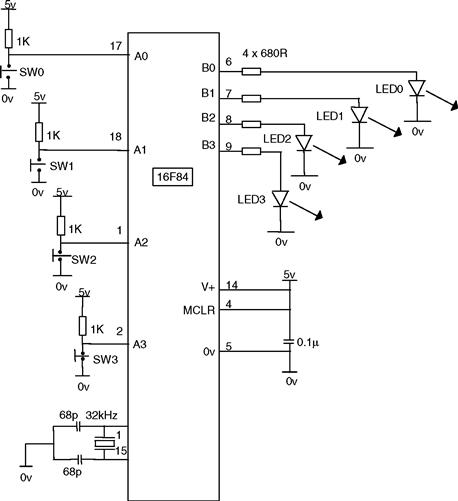
Figure 18.8 The switch scanning circuit
The four switches sw0, sw1, sw2 and sw3 turned on LED0, LED1, LED2 and LED3 respectively.
To test the inputs monitor the voltage on the input pins to the microcontroller, pins 1, 2, 17 and 18. They should go high and low as you throw the switches.
Checking outputs
The microcontroller will output 5v to turn on the outputs.
To make sure the outputs are connected correctly, apply 5v to each output pin in turn to make sure the corresponding LED lights.
When 5v is applied to pin 6, the B0 output then LED0 should light, etc. If it doesn't the resistor value could be incorrect or the LED faulty or in the wrong way round.
Check the oscillator
Check the oscillator is operating by monitoring the signal on CLKOUT, pin 15, with an oscilloscope or counter. Correct selection of the oscillator capacitor values are important – use 68pF with the 16C54 and 16F84 when using a 32kHz crystal.
Has the micro been programmed for the correct oscillator: R-C, LP, XT or HS. Most programs in this book use the LP configuration for the 32kHz Oscillator.
If everything is OK so far then the fault is with the microcontroller chip or the program.
Checking the microcontroller
If the program is not running it could be that you have a faulty microcontroller. You could of course try another, but how do you know if that is a good one or not. The best course of action is to load a program you know works, into the micro. Such as FLASHER.ASM from Chapter 2. This flashes an LED on and off for one second, it doesn't use any inputs and only 1 output B0.
Checking the code
If there are no hardware faults then the problem is in your code.
I find a useful aid is first of all turn an LED on for 1 second and then turn it off. When this works you know that the microcontroller is ok, and that your timing has been set correctly and the oscillator and power supply are functioning correctly. With the switch scanning circuit you could turn all 4 LEDs on for 1 second anyway to serve as an LED check.
To check your code, break it up into sections. Look at were the program stops running to identify the problem area.
If possible turn on LEDs on the outputs to indicate where you are in the program. If you are supposed to turn LED3 on when you go into a certain section of code and LED3 doesn't turn on, then of course you have not gone into that section you are stuck somewhere else.
These instructions can be removed later when the program is working.
Using a simulator
By using a simulator such as the one contained in MPLAB you can single step through the program and check it out a line at a time. To use the simulator from MPLAB select – Debugger, Select Tool, MPLAB SIM as shown in Figure 18.9.

Figure 18.9 Selecting MPLAB SIM
Development kits
There are a number of development kits on the market (and you can make your own). They have a socket for your micro, inputs and outputs that you can connect to your micro. They are ideal for program development. Once verified using the kit if the system does not work then your circuit is at fault. I have developed such a kit shown in Figure 18.10. Details of it can be found on the SL Electrotech website at:

Figure 18.10 PIC microcontroller development kit