
CHAPTER 3
Digital Audio Recording
The hardware design of a digital audio recorder embodies fundamental principles such as sampling and quantizing. The analog signal is sampled and quantized and converted to numerical form prior to storage, transmission, or processing. Subsystems such as dither generator, anti-aliasing filter, sample-and-hold, analog-to-digital converter, and channel code modulator constitute the hardware encoding chain. Although other architectures have been devised, the linear pulse-code modulation (PCM) system is the most illustrative of the nature of audio digitization and is the antecedent of other methods. This chapter and the next, focus on the PCM hardware architecture. Such a system accomplishes the essential pre- and postprocessing for either a digital audio recorder or a real-time digital processor.
The bandwidth of a recording or transmission medium measures the range of frequencies it is able to accommodate with an acceptable amplitude loss. An audio signal sampled at a frequency of 48 kHz and quantized with 16-bit words comprises 48 kHz × 16 bits, or 768 kbps (thousand bits per second). With overhead for data such as synchronization, error correction, and modulation, the channel bit rate might be 1 Mbps (million bits per second) for a monaural audio channel. Clearly, unless bit-rate reduction is applied, considerable throughput capacity is needed for digital audio recording and transmission. It is the task of the digital recording stage to encode the audio signal with sufficient fidelity, while maintaining an acceptable bit rate.
Pulse-Code Modulation
Modulation is a means of encoding information for purposes such as transmission or storage. In theory, many different modulation techniques could be used to digitally encode audio signals. These techniques are fundamentally identical in their task of representing analog signals as digital data, but in practice they differ widely in relative efficiency and performance. Techniques such as amplitude modulation (AM) and frequency modulation (FM) have long been used to modulate carrier frequencies with analog audio information for radio broadcast. Because these are continuous kinds of modulation, they are referred to as wave-parameter modulation.
When conveying sampled information, various types of pulse modulation present themselves. For example, a pulse width or pulse position in time might represent the signal amplitude at sample time; pulse-width modulation (PWM) is an example of the former, and pulse-position modulation (PPM) is an example of the latter. In both cases, the original signal amplitude is coded and conveyed through constant-amplitude pulses. A signal’s amplitude can also be conveyed directly by pulses; pulse-amplitude modulation (PAM) is an example of this approach. The amplitude of the pulses equals the amplitude of the signal at sample time. PWM, PPM, and PAM are shown in Figs. 3.1A through D. In other cases, sample amplitudes are conveyed through numerical methods. For example, in pulse-number modulation (PNM), the modulator generates a string of pulses; the pulse count represents the amplitude of the signal at sample time; this is shown in Fig. 3.1F. However, for high resolution, a large number of pulses are required. Although PWM, PPM, PAM, and PNM are often used in the context of conversion, they are not suitable for transmission or recording because of error or bandwidth limitations.
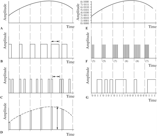
FIGURE 3.1 PWM, PPM, and PAM are examples of pulse-parameter modulation. PNM and PCM are examples of numerical pulse parameter modulation. A. Analog waveform. B. Pulse-width modulation. C. Pulse-position modulation. D. Pulse-amplitude modulation. E. Quantized analog waveform. F. Pulse-number modulation. G. Pulse-code modulation.
The most commonly used modulation method is pulse-code modulation (PCM). PCM was devised in 1937 by Alec Reeves while he was working as an engineer at the International Telephone and Telegraph Company laboratories in France. (Reeves also invented PWM.) In PCM, the input signal undergoes sampling, quantization, and coding. By representing the measured analog amplitude of samples with a pulse code, binary numbers can be used to represent amplitude. At the receiver, the pulse code is used to reconstruct an analog waveform. The binary words that represent sample amplitudes are directly coded into PCM waveforms as shown in Fig. 3.1G.
With methods such as PWM, PPM, and PAM, only one pulse is needed to represent the amplitude value, but in PCM several pulses per sample are required. As a result, PCM might require a channel with higher bandwidth. However, PCM forms a very robust signal in that only the presence or absence of a pulse is necessary to read the signal. In addition, a PCM signal can be regenerated without loss. Therefore the quality of a PCM transmission depends on the quality of the sampling and quantizing processes, not the quality of the channel itself. In addition, depending on the sampling frequency and capacity of the channel, several PCM signals can be combined and simultaneously conveyed with time-division multiplexing. This expedites the use of PCM; for example, stereo audio is easily conveyed. Although other techniques presently exist and newer ones will be devised, they will measure their success against that of pulse-code modulation digitization. In most cases, highly specialized channel codes are used to modulate the signal prior to storage. These channel modulation codes are also described in this chapter.
The architecture of a linear PCM (sometimes called LPCM) system closely follows a readily conceptualized means of designing a digitization system. The analog waveform is filtered and time sampled and its amplitude is quantized with an analog-to-digital (A/D) converter. Binary numbers are represented as a series of modulated code pulses representing waveform amplitudes at sample times. If two channels are sampled, the data can be multiplexed to form one data stream. Data can be manipulated to provide synchronization and error correction, and auxiliary data can be added as well. Upon playback, the data is demodulated, decoded, and error-corrected to recover the original amplitudes at sample times, and the analog waveform is reconstructed with a digital-to-analog (D/A) converter and lowpass filter.
The encoding section of a conventional stereo PCM recorder consists of input amplifiers, a dither generator, input lowpass filters, sample-and-hold circuits, analog-to-digital converters, a multiplexer, digital processing and modulation circuits, and a storage medium such as an optical disc or a hard-disk drive. An encoding section block diagram is shown in Fig. 3.2. This hardware design is a practical realization of the sampling theorem. In practice, other techniques such as oversampling may be employed.
An audio digitization system is really nothing more than a transducer, which processes the audio signal for digital storage or transmission, then processes it again for reproduction. Although that sounds simple, the hardware must be carefully engineered; the quality of the reproduced audio depends entirely on the system’s design. Each subsystem must be carefully considered.
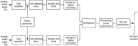
FIGURE 3.2 A linear PCM record section showing principal elements.
Dither Generator
Dither is a noise signal added to the input audio signal to remove quantization artifacts. As described in Chap. 2, dither causes the audio signal to vary between adjacent quantization levels. This action decorrelates the quantization error from the signal, removes the effects of the error, and encodes signal amplitudes below the amplitude of a quantization increment. However, although it reduces distortion, dither adds noise to the audio signal. Perceptually, dither is beneficial because noise is more readily tolerated by the ear than distortion.
Analog dither, applied prior to A/D conversion, causes the A/D converter to make additional level transitions that preserve low-level signals through duty cycle, or pulse-width modulation. This linearizes the quantization process. Harmonic distortion products, for example, are converted to wideband noise. Several types of dither signals, such as Gaussian, rectangular, and triangular probability density functions can be selected by the designer; in some systems, the user is free to choose a dither signal. The amplitude of the applied dither is also critical. In some cases, the input signal might have a high level of residual noise. For example, an analog preamplifier might have a noise floor sufficient to dither the quantizer. However, the digital system must provide a dynamic range that sufficiently captures all the analog information, including the signal within the analog noise floor, and must not introduce quantization distortion into it. The word length of the quantizer must be sufficient for the audio program, and its least significant bit (LSB) must be appropriately dithered. In addition, whenever the word length is reduced, for example, when a 20-bit master recording is transferred to the 16-bit format, dither must be applied, as well as noise shaping. Dither is discussed more fully in Chap. 2; psychoacoustically optimized noise shaping is described in Chap. 18.
Input Lowpass Filter
An input audio signal might have high-frequency content that is above the Nyquist (half-sampling) frequency. To ensure that the Nyquist theorem is observed, and thus prevent aliasing, digital audio systems must bandlimit the audio input signal, eliminating high-frequency content above the Nyquist frequency. This can be accomplished with an input lowpass filter, sometimes called an anti-aliasing filter. In a system with a sampling frequency of 48 kHz, the ideal filter cutoff frequency would be 24 kHz. The input lowpass filter must attenuate all signals above the half-sampling frequency, yet not affect the lower in-band signals. Thus, an ideal filter is one with a flat passband, an immediate or brick-wall filter characteristic, and an infinitely attenuated stopband, as shown in Fig. 3.3A. In addition to these frequency-response criteria, an ideal filter must not affect the phase linearity of the signal.
Although in practice an ideal filter can be approximated, its realization presents a number of engineering challenges. The filter’s passband must have a flat frequency response; in practice some frequency irregularity (ripple) exists, but can be minimized. The stopband attenuation must equal or exceed the system’s dynamic range, as determined by the word length. For example, a 16-bit system would require stopband attenuation of over −95 dB; a stopband attenuation of −80 dB would yield 0.01% alias distortion under worst-case conditions. Modern A/D converters use digital filtering and oversampling methods to perform anti-aliasing; this is summarized later in this chapter, and described in detail in Chap. 18. Early systems used only analog input lowpass filters. Because they clearly illustrate the function of anti-aliasing filtering, and because even modern converters still employ low-order analog filters, analog lowpass filters are described below.
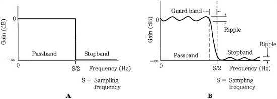
FIGURE 3.3 Lowpass filter characteristics. A. An ideal lowpass filter has a flat passband response and instantaneous cutoff. B. In practice, filters exhibit ripple in the stopband and passband, and sloping cutoff.
In early systems (as opposed to modern systems that use digital filters) the input signal is lowpass filtered by an analog filter with a very sharp cutoff to bandlimit the signal to frequencies at or below the half-sampling frequency. A brick-wall cutoff demands compromise on specifications such as flat passband and low phase distortion. To alleviate the problems such as phase nonlinearities created by a brick-wall response, analog filters can use a more gradual cutoff. However, a low-order filter with a cutoff at the half-sampling frequency would roll off audio frequencies, hence its passband must be extended to a higher frequency. To avoid aliasing, the sampling frequency must be extended to ensure that the filter provides sufficient attenuation at the half-sampling frequency. A higher sampling frequency, perhaps three times higher than required for a brick-wall filter, might be needed; however, this would raise data bandwidth requirements. To limit the sampling frequency and make full use of the passband below the half-sampling point, a brick-wall filter is mandated. When a sampling frequency of 48 kHz is used, the analog input filters are designed for a flat response from dc to 22 kHz. This arrangement provides a guard band of 2 kHz to ensure that attenuation is sufficient at the half-sampling point. A practical lowpass filter characteristic is shown in Fig. 3.3B.
Several important analog filter criteria are overshoot, ringing, and phase linearity. Sharp cutoff filters exhibit resonance near the cutoff frequency and this ringing can cause irregularity in the frequency response. The sharper the cutoff, the greater the propensity to ringing. Certain filter types have inherently reduced ringing. Phase response is also a factor. Lowpass filters exhibit a frequency-dependent delay, called group delay, near the cutoff frequency, causing phase distortion. This can be corrected with an analog circuit preceding or following the filter, which introduces compensating delay to achieve overall phase linearity; this can yield a pure delay, which is inaudible. In the cases of ringing and group delay, there is debate on the threshold of audibility of such effects; it is unclear how perceptive the ear is to such high-frequency phenomena.
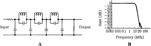
FIGURE 3.4 An example of a Chebyshev lowpass filter and its frequency response. A. A passive lowpass filter schematic. B. Lowpass filter frequency response showing a steep cutoff.
Analog filters can be classified according to the mathematical polynomials that describe their characteristics. There are many filter types; for example, Bessel, Butter-worth, and Chebyshev filters are often used. For each of these filter types, a basic design stage can be repeated or cascaded to increase the filter’s order and to sharpen the cutoff slope. Thus, higher-order filters more closely approximate a brick-wall frequency response. For example, a passive Chebyshev lowpass filter is shown in Fig. 3.4; its cutoff slope becomes steeper when the filter’s order is increased through cascading. However, phase shift also increases as the filter order is increased. The simplest lowpass filter is a cascade of RC (resistor-capacitor) sections; each added section increases the roll-off slope by 6 dB/octave. Although the filter will not suffer from overshoot and ringing, the passband will exhibit frequency response anomalies.
Resonant peaks can be positioned just below the cutoff frequency to smooth the passband response of a filter but not affect the roll-off slope; a Butterworth design accomplishes this. However, a high-order filter is required to obtain a sharp cutoff and deep stopband. For example, a design with a transition band 40% of an octave wide and a stopband of −80 dB would require a 33rd-order Butterworth filter.
A filter with a narrow transition band can be designed at the expense of passband frequency response. This can be achieved by placing the resonant peaks somewhat higher than in a Butterworth design. This is the aim of a Chebyshev filter. A 9th-order Chebyshev filter can achieve a ±0.1-dB passband ripple to 20 kHz, and stopband attenuation of −70 dB at 25 kHz.
One characteristic of most filter types is that attenuation continues past the necessary depth for frequencies beyond the half-sampling frequency. If the attenuation curve is flattened, the transition band can be reduced. Anti-resonant notches in the stopband are often used to perform this function. In addition, reactive elements can be shared in the design, providing resonant peaks and anti-resonant notches. This reduces circuit complexity. The result is called an elliptical, or Cauer filter. An elliptical filter has the steepest cutoff for a given order of realization. For example, a 7th-order elliptical filter can provide a ±0.25-dB passband ripple, 40% octave transition band, and a −80-dB stopband. In practice, a 13-pole design might be required.
In general, for a given analog filter order, Chebyshev and elliptical lowpass filters give a closer approximation to the ideal than Bessel or Butterworth filters, but Chebyshev filters can yield ripple in the passband and elliptical filters can produce severe phase nonlinearities. Bessel filters can approximate a pure delay and provide excellent phase response; however, a higher-order filter is needed to provide a very high rate of attenuation. Butterworth filters are usually flat in the passband, but can exhibit slow transient response. No analog filter is ideal, and there is a trade-off between a high rate of attenuation and an acceptable time-domain response.
In practice, as noted, because of the degradation introduced by analog brick-wall filters, all-analog designs have been superseded by A/D converters that employ a low-order analog filter, oversampling, and digital filtering as discussed later in this chapter and described in detail in Chap. 18. Whatever method is used, an input filter is required to prevent aliasing of any frequency content higher than the Nyquist frequency.
Sample-and-Hold Circuit
As its name implies, a sample-and-hold (S/H) circuit performs two simple yet critical operations. It time-samples the analog waveform at a periodic rate, putting the sampling theorem into practice. It also holds the analog value of the sample while the A/D converter outputs the corresponding digital word. This is important because otherwise the analog value could change after the designated sample time, causing the A/D converter to output incorrect digital words. The input and output responses of an S/H circuit are shown in Fig. 3.5. The output signal is an intermediate signal, a discrete PAM staircase representing the original analog signal, but is not a digital word. The circuit is relatively simple to design; however, it must accomplish both of its tasks accurately. Samples must be captured at precisely the correct time and the held value must stay within tolerance. In practice, the S/H function is built into the A/D converter. The S/H circuit is also known as a track-hold circuit.
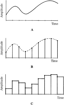
FIGURE 3.5 The sample-and-hold circuit captures an analog value and holds it while A/D conversion occurs. A. Analog input signal. B. Sampled input. C. Analog held output.
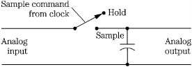
FIGURE 3.6 A conceptual sample-and-hold circuit contains a switch and storage element. The switch is closed to sample the signal.
As we have seen, time and amplitude information can completely characterize an acoustic waveform. The S/H circuit is responsible for capturing both informational aspects from the analog waveform. Samples are taken at a periodic rate and reproduced at the same periodic rate. The S/H circuit accomplishes this time sampling. A clock, an oscillator circuit that outputs timing pulses, is set to the desired sampling frequency, and this command signal controls the S/H circuit.
Conceptually, an S/H circuit is a capacitor and a switch. The circuit tracks the analog signal until the sample command causes the digital switch to isolate the capacitor from the signal; the capacitor holds this analog voltage during A/D conversion. A conceptual S/H circuit is shown in Fig. 3.6. The S/H circuit must have a fast acquisition time that approaches zero; otherwise, the value output from the A/D converter will be based on an averaged input over the acquisition time, instead of the correct sample value at an instant in time. In addition, varying sample times result in acquisition timing error; to prevent this, the S/H circuit must be carefully designed and employ a sample command that is accurately clocked.
Jitter is any variation in absolute timing; in this case, variation in the sampling signal is shown in Fig. 3.7. Jitter adds noise and distortion to the sampled signal, and must be limited in the clock used to switch the S/H circuit. Jitter is particularly significant in the case of a high-amplitude, high-frequency input signal. The timing precision required for accurate A/D conversion is considerable. Depending on the converter design, for example, jitter at the S/H circuit must be less than 200 ps (picosecond) to allow 16-bit accuracy from a full amplitude, 20-kHz sine wave, and less than 100 ps for 18-bit accuracy. Only then would the resulting noise components fall below the quantization noise floor. Clearly, S/H timing must be controlled by a clock designed with a highly accurate crystal quartz oscillator. Jitter is discussed in Chap. 4.
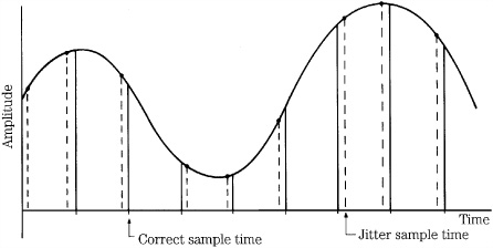
FIGURE 3.7 Jitter is a variation in sample times that can add noise and distortion to the output analog signal.
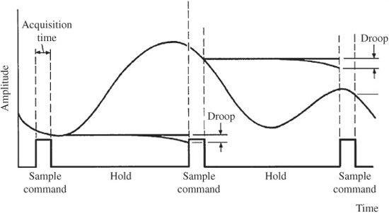
FIGURE 3.8 Acquisition time and droop are two error conditions in the sample-and-hold circuit.
Acquisition time is the time between the initiation of the sample command and the taking of the sample. This time lag can result in a sampled value different from the one present at the correct sample time. The effect of the delay is a function of the amplitude of the analog signal. It is therefore important to minimize acquisition time. The S/H circuit’s other primary function is to hold the captured analog voltage while conversion takes place. This voltage must remain constant because any variation greater than a quantization increment can result in an error at the A/D output. The held voltage can be prone to droop because of current leakage. Droop is the decrease in hold voltage as the storage capacitor leaks between sample times. Care in circuit design and selection of components can limit droop to less than one-half a quantization increment over a 20-μs period. For example, a 16-bit, ±10-V range A/D converter must hold a constant value to within 1 mV during conversion. Acquisition time error and droop are illustrated in Fig. 3.8.
The demands of fast acquisition time and low droop are in conflict in the design of a practical S/H circuit. For fast acquisition time, a small capacitor value is better, permitting faster charging time. For droop, however, a large-valued capacitor is preferred, because it is better able to retain the sample voltage at a constant level for a longer time. However, capacitor values of approximately 1 nF can satisfy both requirements. In addition, high-quality capacitors made of polypropylene or Teflon dielectrics can be specified. These materials can respond quickly, hold charge, and minimize dielectric absorption and hysteresis—phenomena that cause voltage variations.
In practice, an S/H circuit must contain more than a switch and a capacitor. Active circuits such as operational amplifiers must buffer the circuit to condition the input and output signals, speed switching time, and help prevent leakage. Only a few specialized operational amplifiers meet the required specifications of large bandwidth and fast settling time. Junction field-effect transistor (JFET) operational amplifiers usually perform best. Thus, a complete S/H circuit might have a JFET input operational amplifier to prevent source loading, improve switching time, isolate the capacitor, and supply capacitor-charging current. The S/H switch itself may be a JFET device, selected to operate cleanly and accurately with minimal jitter, and the capacitor may exhibit low hysteresis. A JFET operational amplifier is usually placed at the output to help preserve the capacitor’s charge.
Analog-to-Digital Converter
The analog-to-digital (A/D) converter lies at the heart of the encoding side of a digital audio system, and is perhaps the single most critical component in the entire signal chain. Its counterpart, the digital-to-analog (D/A) converter, can subsequently be improved for higher fidelity playback. However, errors introduced by the A/D converter will accompany the audio signal throughout digital processing and storage and, ultimately, back into its analog state. Thus the choice of the A/D converter irrevocably affects the fidelity of the resulting signal.
Essentially, the A/D converter must examine the sampled input signal, determine the quantization level nearest to the sample’s value, and output the binary code that is assigned to that level—accomplishing those tasks in one sampling period (20 μs for a 48-kHz sampling frequency). The precision required is considerable: 15 parts per million for 16-bit resolution, 4 parts per million for 18-bit resolution, and 1 part per million for 20-bit resolution. In a traditional A/D design, the input analog voltage is compared to a variable reference voltage within a feedback loop to determine the output digital word; this is known as successive approximation. More common oversampling A/D converters are summarized in this chapter and discussed in detail in Chap. 18.
The A/D converter must perform a complete conversion on each audio sample. Furthermore, the digital word it provides must be an accurate representation of the input voltage. In a 16-bit successive approximation converter, each of the 65,536 intervals must be evenly spaced throughout the amplitude range, so that even the least significant bit in the resulting word is meaningful. Thus, speed and accuracy are key requirements for an A/D converter. Of course, any A/D converter will have an error of ±1/2 LSB, an inherent limitation of the quantization process itself. Furthermore, dither must be applied.
The conversion time is the time required for an A/D converter to output a digital word; it must be less than one sampling period. Achieving accurate conversion from sample to sample is sometimes difficult because of settling time or propagation time errors. The result of accomplishing one conversion might influence the next. If a converter’s input moves from voltage A to B and then later from C to B, the resulting digital output for B might be different because of the device’s inability to properly settle in preparation for the next measurement. Obviously, dynamic errors grow more severe with demand for higher conversion speed. In practice, speeds required for low noise and distortion can be achieved. Indeed, many A/D converters simultaneously process two waveforms, alternating between left and right channels. Other converters can process 5.1 channels of input audio signals.
Numerous specifications have been devised to evaluate the performance accuracy of A/D converters. Amplitude linearity compares output versus input linearity. Ideally, the output value should always correspond exactly with input level, regardless of level. To perform the test, a series of tones of decreasing amplitude, or a fade-to-zero tone, is input to the converter. The tone is dithered with rectangular pdf dither. A plot of device gain versus input level will reveal any deviations from a theoretically flat (linear) response.
Integral linearity measures the “straightness” of the A/D converter output. It describes the transition voltage points, the analog input voltages at which the digital output changes from one code to the next, and specifies how close they are to a straight line drawn through them. In other words, integral linearity determines the deviation of an actual bit transition from the ideal transition value, at any level over the range of the converter. Integral linearity is illustrated in Fig. 3.9A. Integral linearity is tested, and the reference line is drawn across the converter’s full output range. Integral linearity is the most important A/D specification and is not adjustable. An n-bit converter is not a true n-bit converter unless it guarantees at least ±1/2 LSB integral linearity. The converter in Fig. 3.9A has a ±1/4 LSB integral linearity.
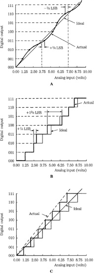
FIGURE 3.9 Performance of an A/D converter can be specified in a variety of ways. A. Integral linearity specification of an A/D converter. B. Differential linearity specification of an A/D converter. C. Absolute accuracy specification of an A/D converter.
Differential linearity error is the difference between the actual step height and the ideal value of 1 LSB. It can be measured as the distance between transition voltages, that is, the widths of individual input voltage steps. Differential linearity is shown in Fig. 3.9B. Ideally, all the steps of an A/D transfer function should be 1 LSB wide. A maximum differential linearity error of ±1/2 LSB means that the input voltage might have to increase or decrease as little as 1/2 LSB or as much as 1 1/2 LSB before an output transition occurs. If this specification is exceeded, to perhaps ±1 LSB, some steps could be 2 LSBs wide and others could be 0 LSB wide; in other words, some output codes would not exist. High-quality A/D converters are assured of having no missing codes over a specified temperature range. The converter in Fig. 3.9B has an error of ±1/2 LSB; some levels are 1/4 LSB wide, others are 1 1/2 LSB wide. Conversion speed can affect both integral linearity and differential linearity errors. Quality A/D converters are guaranteed to be monotonic; that is, the output code either increases or remains the same for increasing analog input signals. If differential error is greater than 1 LSB, the converter will be nonmonotonic.
Absolute accuracy error, shown in Fig. 3.9C, is the difference between the ideal level at which a digital transition occurs and where it actually occurs. A good A/D converter should have an error of less than ±1/2 LSB. Offset error, gain error, or noise error can affect this specification. For the converter in Fig. 3.9C, each interval is 1/8 LSB in error. In practice, otherwise good successive approximation A/D converters can sometimes drift with temperature variations and thus introduce inaccuracies.
Code width, sometimes called quantum, is the range of analog input values for which a given output code will occur. The ideal code width is 1 LSB. A/D converters can exhibit an offset error as well as a gain error. An A/D converter connected for unipolar operation has an analog input range from 0 V to positive full scale. The first output code transition should occur at an analog input value of 1/2 LSB above 0 V. Unipolar offset error is the deviation of the actual transition value from the ideal value. When connected in a bipolar configuration, bipolar offset is set at the first transition value above the negative full-scale value. Bipolar offset error is the deviation of the actual transition value from the ideal transition value at 1/2 LSB above the negative full-scale value. Gain error is the deviation of the actual analog value at the last transition point from the ideal value, where the last output code transition occurs for an analog input value 1 1/2 LSB below the nominal positive full-scale value. In some converters, gain and offset errors can be trimmed at the factory, and might be further zeroed with the use of external potentiometers. Multiturn potentiometers are recommended for minimum drift over temperature and time.
Harmonic distortion is a familiar way to characterize audio linearity and can be used to evaluate A/D converter performance. A single pure sine tone is input to the device under test, and the output is examined for spurious content other than the sine tone. In particular, spectral analysis will show any harmonic multiples of the input frequency. Total harmonic distortion (THD) is the ratio of the summed root mean square (rms) voltage of the harmonics to that of the input signal. To further account for noise in the output, the measurement is often called THD+N. The figure is usually expressed as a decibel figure or a percentage; however, visual examination of the displayed spectral output is a valuable diagnostic. It is worth noting that in most analog systems, THD+N decreases as the signal level decreases. The opposite is true in digital systems. Therefore, THD+N should be specified at both high and low signal levels. THD+N should be evaluated versus amplitude and versus frequency, using FFT analysis.
Dynamic range can also be used to evaluate converter performance. Dynamic range is the amplitude range between a maximum-level signal and the noise floor. Using the EIAJ specification, dynamic range is typically measured by reading THD+N at an input amplitude of −60 dB; the negative value is inverted and added to 60 dB to obtain dynamic range. Also, signal-to-noise ratio (examining idle channel noise) can be measured by subtracting the idle noise from the full-scale signal. For consistency, a standard test sequence such as the ITU CCITT 0.33.00 (monaural) and CCITT 0.33.01 (stereo) can be used; these comprise a series of tones and are useful for measuring parameters such as frequency response, distortion, and signal to noise. Noise modulation is another useful measurement. This test measures changes in the noise floor relative to changes in signal amplitude; ideally, there should be no correlation. In practice, because of low-level nonlinearity in the converter, there may be audible shifts in the level or tonality of the background noise that correspond to changes in the music signal. Precisely because the shifts are correlated to the music, they are potentially much more perceptible than benign unchanging noise. In one method used to observe noise modulation, a low-frequency sine tone is input to the converter; the sine tone is removed at the output and the spectrum of the output signal is examined in 1/3-octave bands. The level of the input signal is decreased in 5-dB steps and the test is repeated. Deviation in the noise floor by more than a decibel in any band across the series of tested amplitudes may indicate potentially audible noise modulation.
As noted, an A/D converter is susceptible to jitter, a variation in the timebase of the clocking signal. Random-noise jitter can raise the noise floor and periodic jitter can create sidebands, thus raising distortion levels. Generally, the higher the specified dynamic range of the converter, the lower the jitter level. A simple way to test an A/D converter for jitter limitations is to input a 20-kHz, 0-dBFS (full-amplitude) sine tone, and observe an FFT of the output signal. Repeat with a 100-Hz sine tone. An elevated noise floor at 20 kHz compared to 100 Hz indicates a potential problem from random-noise jitter, and discrete frequencies at 20 kHz indicate periodic jitter. High-quality A/D converters contain internal clocks that are extremely stable, or when accepting external clocks, have clock recovery circuitry to reject jitter disturbance. It is incorrect to assume that one converter using a low-jitter clock will necessarily perform better than another converter using a high-jitter clock; actual performance depends very much on converter design. Even when jitter causes no data error, it can cause sonic degradation. Its effect must be carefully assessed in measurements and listening tests. Jitter is discussed in more detail in Chap. 4.
The maximum analog signal level input to an A/D converter should be scaled as close as possible to the maximum input conversion range, to utilize the converter’s maximum signal resolution. Generally, a converter can be driven by a very low impedance source such as the output of a wideband, fast-settling operational amplifier. Transitions in a successive approximation A/D converter’s input current might be caused by changes in the output current of the internal D/A converter as it tests bits. The output voltage of the driving source must remain constant while supplying these fast current changes.
Changes in the dc power supply can affect an A/D converter’s accuracy. Power supply deviations can cause changes in the positive full-scale value, resulting in a proportional change in all code transition values, that is, a gain error. Normally, regulated power supplies with 1% or less ripple are recommended. Power supplies should be bypassed with a capacitor—for example, 1 to 10 μF tantalum—located near the converter, to obtain noise-free operation. Noise and spikes from a switching power supply must be carefully filtered. To minimize jitter effects, accurate crystal clocks must be used to clock all A/D and S/H circuits.
Sixteen-bit resolution was formerly the quality benchmark for most digital audio devices, and it can yield excellent audio fidelity. However, many digital audio devices now process or store more than 16 bits. A digital signal processing (DSP) chip might internally process 56-bit words; this resolution is needed so that repetitive calculations will not accumulate error that could degrade audio fidelity. In addition, for example, Blu-ray discs can store 20- or 24-bit words. Thus, many A/D and D/A converters claim conversion of up to 24 bits. However, it is difficult or impossible to achieve true 24-bit conversion resolution with current technology. A resolution of 24 bits ostensibly yields a quantization error floor of about −145 dBFS (dB Full Scale). If a dBFS of 2 V rms is used, then a level at −145 dBFS corresponds to about 0.1 μV rms. This is approximately the level of thermal noise in a 6-ohm resistor at room temperature. The ambient noise in any practical signal chain would preclude ideal 24-bit resolution. Internal processing does require longer word lengths, but it is unlikely that A/D or D/A converters will process signals at such high resolution.
Successive Approximation A/D Converter
There are many types of A/D converter designs appropriate for various applications. For audio digitization, the necessity for both speed and accuracy limits the choices to a few types. The successive approximation register (SAR) A/D converter (sometimes known as a residue converter) is a classical method for achieving good-quality audio digitization; a SAR converter is shown in Fig. 3.10. This converter uses a D/A converter in a feedback loop, a comparator, and a control section. In essence, the converter compares an analog voltage input with its interim digital word converted to a second analog voltage, adjusting its interim conversion until the two agree within the given resolution. The device follows an algorithm that, bit by bit, sets the output digital word to match the analog input.
For example, consider an analog input of 6.92 V and an 8-bit SAR A/D converter. The operational steps of SAR conversion are shown in Fig. 3.11. The most significant bit in the SAR is set to 1, with the other bits still at 0; thus the word 10000000 is applied to the internal D/A converter. This word places the D/A converter’s output at its half value of 5 V. Because the input analog voltage is greater than the D/A converter’s output, the comparator remains high. The first bit is stored at logical 1. The next most significant bit is set to 1 and the word 11000000 is applied to the D/A converter, with an interim output of 7.5 V. This voltage is too high, so the second bit is reset to 0 and stored. The third bit is set to 1, and the word 10100000 is applied to the D/A converter; this produces 6.25 V, so the third bit remains high. This process continues until the LSB is stored and the digital word 10110001, representing a converted 6.91 V, is output from the A/D converter.
This successive approximation method requires n D/A conversions for every one A/D conversion, where n is the number of bits in the output word. In spite of this recursion, SAR converters offer relatively high conversion speed. However, the converter must be precisely designed. For example, a 16-bit A/D converter ranging over ±10 V with 1/2-LSB error requires a conversion accuracy of 3 mV. A 10-V step change in the D/A converter must settle to within 0.001% during a period of 1 μs. This period corresponds to an analog time constant of about 100 ns. The S/H circuit must be designed to minimize droop to ensure that the LSB, the last bit output to the SAR register, is accurate within this specification.
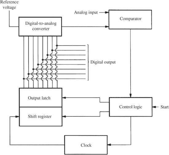
FIGURE 3.10 A successive approximation register A/D converter showing an internal D/A converter and comparator.
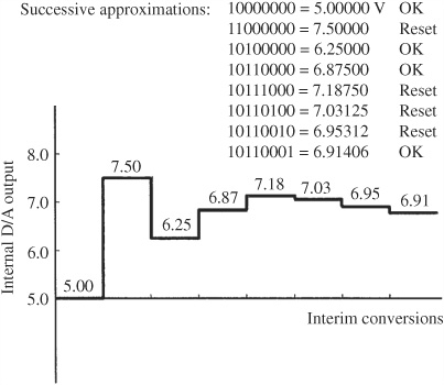
FIGURE 3.11 The intermediate steps in an SAR conversion showing results of interim D/A conversions.
Oversampling A/D Converter
As noted, analog lowpass filters suffer from limitations such as noise, distortion, group delay, and passband ripple; unless great care is taken, it is difficult for downstream A/D converters to achieve resolution beyond 18 bits. In most applications, brick-wall analog anti-aliasing filters and SAR A/D converters have been replaced by oversampling A/D converters with digital filters. The implementation of a digital anti-aliasing filter is conceptually intriguing because the analog signal must be sampled and digitized prior to any digital filtering. This conundrum has been resolved by clever engineering; in particular, a digital decimation filter is employed and combined with the task of A/D conversion. The fundamentals of oversampling A/D conversion are presented here.
In oversampling A/D conversion, the input signal is first passed through a mild analog anti-aliasing filter which provides sufficient attenuation, but only at a high half-sampling frequency. To extend the Nyquist frequency, the filtered signal is sampled at a high frequency and then quantized. After quantization, a digital low-pass filter uses decimation to both reduce the sampling frequency to a nominal rate and prevent aliasing at the new, lower sampling frequency. Quantized data words are output at a lower frequency (for example, 48 or 96 kHz). The decimation low-pass filter removes frequency components beyond the Nyquist frequency of the output sampling frequency to prevent aliasing when the output of the digital filter is resampled (undersampled) at the system’s sampling frequency.
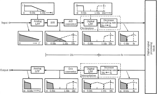
FIGURE 3.12 A two-times oversampling A/D and D/A conversion system. Decimation and interpolation digital filters increase and decrease the sampling frequency while removing alias and image signal components.
Consider the oversampling A/D converter and D/A converter (both using two-times oversampling) shown in Fig. 3.12. An analog anti-aliasing filter restricts the bandwidth to 1.5fs, where fs is the sampling frequency. The relatively wide transition band, from 0.5 to 1.5fs, is acceptable and promotes good phase response. For example, a 7th-order Butterworth filter could be used. The signal is sampled and held at 2fs, and then converted. The digital filter limits the signal to 0.5fs. With decimation, the sampling frequency of the signal is undersampled and hence reduced from 2fs to fs. This action is accomplished with a linear-phase finite impulse response (FIR) digital filter with uniform group delay characteristics. Upon playback, an oversampling filter doubles the sampling frequency, samples are converted to yield an analog waveform, and high-frequency images are removed with a low-order lowpass filter.
Many oversampling A/D converters use a very high initial sampling frequency (perhaps 64- or 128-times 44.1 kHz), and take advantage of that high rate by using sigma-delta conversion of the audio signal. Because the sampling frequency is high, word lengths of one or a few bits can provide high resolution. A sigma-delta modulator can be used to perform noise shaping to lower audio band quantization noise. A decimation filter is used to convert the sigma-delta coding to 16-bit (or higher) coding, and a lower sampling frequency. Consider an example in which one-bit coding takes place at an oversampling rate R of 72; that is, 72 × 44.1 kHz = 3.1752 MHz, as shown in Fig. 3.13. The decimation filter provides a stopband from 20 kHz to the half-sampling frequency of 1.5876 MHz. One-bit A/D conversion greatly simplifies the digital filter design. An output sample is not required for every input bit; because the decimation factor is 72, an output sample is required for every 72 bits input to the decimation filter. A transversal filter can be used, with filter coefficients suited for the decimation factor. Following decimation, the result can be rounded to 16 bits, and output at a 44.1-kHz sampling frequency.
In addition to eliminating brick-wall analog filters, oversampling A/D converters offer other advantages over conventional A/D converters. Oversampling A/D converters can achieve increased resolution compared to SAR methods. For example, they extend the spectrum of the quantization error far outside the audio baseband. Thus the in-band noise can be made quite small. The same internal digital filter that prevents aliasing also removes out-of-band noise components. Increasingly, oversampling A/D converters are employed. This type of sigma-delta conversion is discussed in Chap. 18. Whichever A/D conversion method is used, the goal of digitizing the analog signal is accomplished, as data in two’s complement or other form is output from the device.
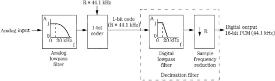
FIGURE 3.13 An oversampling A/D converter using one-bit coding at a high sampling frequency, and a decimation filter.
For digitization systems in which real-time processing such as delay and reverberation is the aim, the signal is ready for processing through software or dedicated hardware. In the case of a digital recording system, further processing is required to prepare the data for the storage medium.
Record Processing
After the analog signal is converted to binary numbers, several operations must occur prior to storage or transmission. Although specific processing needs vary according to the type of output channel, systems generally multiplex the data, perform interleaving, add redundancy for error correction and provide channel coding. Although there is an uninteresting element of bookkeeping in this processing, any drudgery is critical to prepare the data for the output channel and ensure that playback ultimately will be satisfactorily accomplished.
Some digital audio programs are stored or transmitted with emphasis, a simple means of reducing noise in the signal. Pre-emphasis equalization boosts high frequencies prior to storage or transmission. At the output, corresponding de-emphasis equalization attenuates high frequencies. The net result is a reduction in the noise floor. A common emphasis characteristic uses time constants of 50 and 15 μs, corresponding to frequency points at 3183 and 10,610 Hz, with a 6-dB/octave slope between these points, as shown in Fig. 3.14. Use of pre-emphasis must be identified in the program material so that de-emphasis equalization can be applied at the output.
In analog recording, an error occurring during storage or transmission results in degraded playback. In digital recording, error detection and correction minimize the effect of such defects. Without error correction, the quality of digital audio recording would be greatly diminished. Several steps are taken to combat the effects of errors. To prevent a single large defect from destroying large areas of consecutive data, interleaving is employed; this scatters data through the bitstream so the effect of an error is scattered when data is de-interleaved during playback. During encoding, coded parity data is added; this is redundant data created from the original data to help detect and correct errors. A discussion of parity, check codes, redundancy, interleaving, and error correction is presented in Chap. 5.
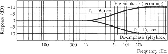
FIGURE 3.14 Pre-emphasis boosts high frequencies during recording, and de-emphasis reduces them during playback to lower the noise floor.
Multiplexing is used to form a serial bitstream. Most digital audio recording and transmission is a serial process; that is, the data is processed as a single stream of information. However, the output of the A/D converter can be parallel data; for example, two 16-bit words may be output simultaneously. A data multiplexer converts this parallel data to serial data; the multiplexing circuit accepts parallel data words and outputs the data one bit at a time, serially, to form a continuous bitstream.
Raw data must be properly formatted to facilitate its recording or transmission. Several kinds of processing are applied to the coded data. The time-multiplexed data code is usually grouped into frames. To prevent ambiguity, each frame is given a synchronization code to delineate frames as they occur in the stream. A synchronization code is a fixed pattern of bits that is distinct from any other coded data bit pattern in much the same way that a comma is distinct from the characters in a sentence. In many cases, data files are preceded by a data header with information defining the file contents.
Addressing or timing data can be added to frames to identify data locations in the recording. This code is usually sequentially ordered and is distributed through the recording to distinguish between different sections. As noted, error correction data is also placed in the frame. Identification codes might carry information pertinent to the playback processing. For example, specification of sampling frequency, use of pre-emphasis, table of contents, timing and track information, and copyright information can be entered into the data stream.
Channel Codes
Channel coding is an important example of a less visible, yet critical element in a digital audio system. Channel codes were aptly described by Thomas Stockham as the handwriting of digital audio. Channel code modulation occurs prior to storage or transmission. The digitized audio samples comprise 1s and 0s, but the binary code is usually not conveyed directly. Rather, a modulated channel code represents audio samples and other conveyed information. It is thus a modulation waveform that is interpreted upon playback to recover the original binary data and thus the audio waveform. Modulation facilitates data reading by further delineating the recorded logical states. Moreover, through modulation, a higher coding efficiency is achieved; although more bits might be conveyed, a greater data throughput can be achieved overall.
Storing binary code directly on a medium is inefficient. Much greater densities with high code fidelity can be achieved through methods in which modulation code fidelity is low. The efficiency of a coding method is the number of data bits transmitted divided by the number of transitions needed to convey them. Efficiencies vary from about 50% to nearly 150%. In light of these requirements, PCM, for example, is not suitable for transmission or recording to a medium such as optical disc; thus, other channel modulation techniques must be devised. Although binary recording is concerned with storing the 0s and 1s of the data stream, the signal actually recorded might be quite different. Typically, it is the transitions from one level to another, rather than the amplitude levels themselves, which represent the channel data. In that respect, the important events in a digitally encoded signal are the instants in time at which the state of the signal changes.
A channel code describes the way information is modulated into a channel signal, stored or transmitted, and demodulated. In particular, information bits are transformed into channel bits. The transfer functions of digital media create a number of specific difficulties that can be overcome through modulation techniques. A channel code should be self-clocking to permit synchronization at the receiver, minimize low-frequency content that could interfere with servo systems, permit high data rate transmission or high-density recording, exhibit a bounded energy spectrum, have immunity to channel noise, and reveal invalid signal conditions. Unfortunately, these requirements are largely mutually conflicting, thus only a few channel codes are suitable for digital audio applications.
The decoding clock in the receiver must be synchronized in frequency and phase with the clock (usually implicit in the channel bit patterns) in the transmitted signal. In most cases, the frames in a binary bitstream are marked with a synchronization word. Without some kind of synchronization, it might be impossible to directly distinguish between the individual channel bits.
Even then, a series of binary 1s or 0s form a static signal upon playback. If no other timing or decoding information is available, the timing information implicitly encoded in the channel bit periods is lost. Therefore, such data must often be recorded in such a way that pulse timing is delineated. Codes that provide a high transition rate, which are suitable for regenerating timing information at the receiver, are called self-clocking codes.
Thus, one goal of channel modulation is to combine a serial data stream with a clock pulse to produce a single encoded waveform that is self-clocking. Generally, code efficiency must be diminished to achieve self-clocking because clocking increases the number of transitions, which increases the overall channel bit rate. The high-frequency signal produced by robust clocking content will decrease a medium’s storage capacity, and can be degraded over long cable runs. A minimum distance between transitions (Tmin) determines the highest frequency in the code, and is often the highest frequency the medium can support. The ratio of Tmin to the length of a single bit period of input information data is called the density ratio (DR). From a bandwidth standpoint, a long Tmin is desirable in a code. Tmax determines the maximum distance between transitions sufficient to support clocking. From a clocking standpoint, a shorter Tmax is desirable.
Time-axis variations such as jitter are characterized by phase variations in a signal, observable as a frequency modulation of a stable waveform. The constraints of channel coding and data regeneration fundamentally limit the maximum number of incremental periods between transitions, that is, the number of transitions that can be detected between Tmin and Tmax. An important consideration in modulation code design is tolerance in locating a transition in the code. This is called the window margin, phase margin, or jitter margin and notated as Tw. It describes the minimum difference between code wavelengths: the larger the clock window, the better the jitter immunity. The efficiency of a code can be measured by its density ratio that is the ratio of the number of information bits to the number of channel transitions. The product of DR and Tw is known as the figure of merit (FoM); by combining density ratio and jitter margin, an overall estimate of performance is obtained: the higher the numerical value of FoM, the better the performance.
An efficient coding format must restrict dc content in the coded waveform, which could disrupt timing synchronization; dc content measures the time that the waveform is at logical 1 versus the time at logical 0; a dc content of 0 is ideal. Generally, digital systems are not responsive to direct current, so any dc component of the transmitted signal may be lost. In addition, dc components result in a baseline offset that reduces the signal-to-noise ratio. The dc content is the fraction of time that the signal is high during a string of 1s or 0s minus the fraction of time it is low. It results in a nonzero average amplitude value. For example, a nonreturn to zero (NRZ) signal (in which binary values are coded as high- or low-signal amplitudes) with all 0s or 1s would give a dc content of 100%.
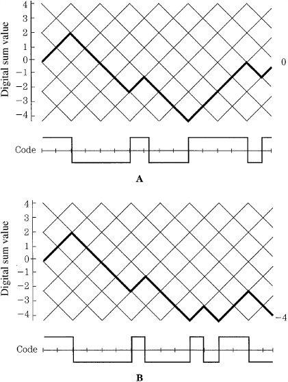
FIGURE 3.15 The digital sum value (DSV) monitors the dc content in a bitstream. A. A coded waveform that is free of dc content over the measured interval. B. A coded waveform that contains dc content.
The dc content can be monitored through the digital sum value (DSV). The DSV of a code can be thought of as the difference in accumulated charge if the code was passed through an ac coupling capacitor. In other words, it shows the dc bias that accumulates in a coded sequence. Figure 3.15 shows two different codes and their DSV; over the measured interval, the first code does not show dc content, the second does. The dc content might cause problems in transformer-coupled magnetic recording heads; magnetic heads sense domains inductively and hence are inefficient in reading low-frequency signals. The dc content can present clock synchronization problems, and lead to errors in the servo systems used for radial tracking and focusing in an optical system. These systems generally operate in the low-frequency region. Low-frequency components in the readout signal cause interference in the servo systems, making them unstable. A dc-free code improves both the bandwidth and signal-to-noise ratio of the servo system. In the Compact Disc format, for example, the frequency range from 20 kHz to 1.5 MHz is used for information transmission; the servo systems operate on signals in the 0- to 20-kHz range.
A single sampling pulse is easy to analyze because of its periodic nature in the time domain; Fourier analysis clearly shows its spectrum. However, a data stream differs in that the data pulses occur aperiodically, and in fact can be considered to be random. The power spectrum density, or power spectrum, shows the response of the data stream. For example, Fig. 3.16 shows the spectral response of three types of channel coding with random data sequences: nonreturn to zero (NRZ), modified frequency modulation (MFM), and biphase. A transmission waveform ideally should have minimal energy at low frequencies to avoid clocking and servo errors, and minimal energy at high frequencies to reduce bandwidth requirements. Biphase codes (there are many types, one being binary FM) yield a spectrum that has a broadband energy distribution. The MFM code exhibits a very narrow spectrum. The MFM and biphase codes are similar because they have no strong frequency components at low frequencies (lower than 0.2f where f = 1/T). If the value of f is 500 kHz, for example, and the servo signals do not extend beyond 15 kHz, these codes would be suitable. The NRZ code has a strong dc content and could pose problems for a servo system.
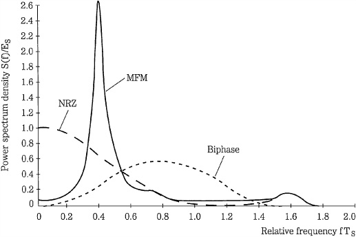
FIGURE 3.16 The power spectral density shows the response of a stream of random data sequences. NRZ code has severe dc content; MFM code exhibits a very narrow spectrum; biphase codes yield a broadband energy distribution.
To minimize decoding errors, formats can be developed in which data is conveyed with data patterns that are as individually unique as possible. For example, in the eight-to-fourteen modulation (EFM) code devised for the Compact Disc format, 8-bit symbols are translated into 14-bit symbols, carefully selected for maximum difference between symbols. In this way, invalid data can be more easily recognized. Similarly, a data symbol could be created based on previous adjacent symbols and the receiver could recognize the symbol and its past history as a unique state. A state pattern diagram is used in which all transitions are defined, based on all possible adjacent symbols.
As noted, in many codes, the information is contained in the timing of transitions, not in the direction (low to high, or high to low) of the transitions. This is advantageous because the code is thus insensitive to polarity; the content will not be affected if the signal is inverted. The EFM code enjoys this property.
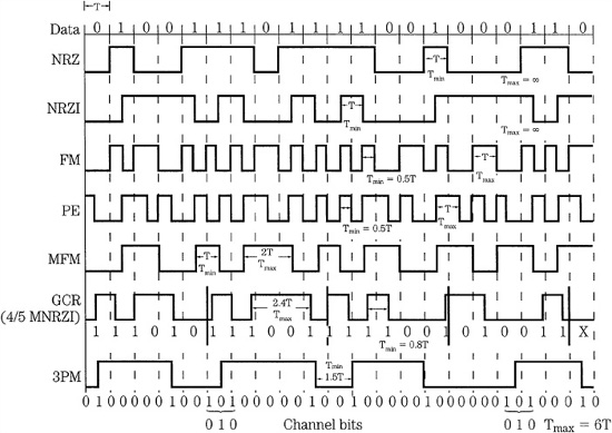
FIGURE 3.17 A comparison of simple and group-code waveforms for a common data input.
Simple Codes
The channel code defines the logical 1 and 0 of the input information. We might assume a direct relationship between a high amplitude and logical 1, and a low amplitude and logical 0. However, many other relationships are possible; for example, in one version of frequency-shift keying (FSK), a logical 1 corresponds to a sine burst of 100 kHz and a logical 0 corresponds to a sine burst of 150 kHz. Methods that use only two values take full advantage of digital storage; relatively large variations in the medium do not affect data recovery. Because digitally stored data is robust, high packing densities can be achieved. Various modulation codes have been devised to encode binary data according to the medium’s properties. Of many, only a few are applicable to digital audio storage, on either magnetic or optical media. A number of channel codes are shown in Fig. 3.17.
Perhaps the most basic code sends a pulse for each 1 and does not send a pulse for a 0; this is called return to zero (RZ) code because the signal level always returns to zero at the end of each bit period.
The nonreturn to zero (NRZ) code is also a basic form of modulation: 1s and 0s are represented directly as high and low levels. The direction of the transition at the beginning or end of a bit period indicates a 1 or 0. The minimum interval is T, but the maximum interval is infinite (when data does not change) thus NRZ suffers from one of the problems that encourages use of modulation: strings of 1s or 0s do not produce transitions in the signal, thus a clock cannot be extracted from the signal. In addition, this creates dc content. The data density (number of bits per transition) for NRZ is 1.
The nonreturn to zero inverted (NRZI) code is similar to the NRZ code, except that only 1s are denoted with amplitude transitions (low to high, or high to low); no transitions occur for 0s. For example, any flux change in a magnetic medium indicates a 1, with transitions occurring in the middle of a bit period. With this method, the signal is immune to polarity reversal. The minimum interval is T, and the maximum is infinite; a clock cannot be extracted. A stream of 1s generates a transition at every clock interval; thus, the signal’s frequency is half that of the clock. A stream of 0s generates no transitions. Data density is 1.
In binary frequency modulation (FM), also known as biphase mark code, there are two transitions for a 1 and one transition for a 0; this is essentially the minimum frequency implementation of FSK. The code is self-clocking. Biphase space code reverses the 1/0 rules. The minimum interval is 0.5T and the maximum is T. There is no dc content and the code is invertible. In the worst case, there are two transitions per bit, yielding a density ratio of 0.5, or an efficiency of 50%. FoM is 0.25. This code is used in the AES3 standard, described in Chap. 13.
In phase encoding (PE), also known as phase modulation (PM), biphase level modulation or Manchester code, a 1 is coded with a negative-going transition, and a 0 is coded with a positive-going transition. Consecutive 1s or 0s follow the same rule, thus requiring an extra transition. These codes follow phase-shift keying techniques. The minimum interval is 0.5T and the maximum is T. This code does not have dc content, and is self-clocking. Density ratio is 0.5. The code is not invertible.
In modified frequency modulation (MFM) code, sometimes known as delay modulation or Miller code, a 1 is coded with either a positive- or negative-going transition in the center of a bit period, for each 1. There is no transition for 0s; rather, a transition is performed at the end of a bit period only if a string of 0s occurs. Each information bit is coded as two channel bits. There is a maximum of three 0s and a minimum of one 0 between successive 1s. In other words, d = 1 and k = 3. The minimum interval is T and the maximum is 2T. The code is self-clocking, and can have dc content. Density ratio is 1 and FoM is 0.5.
Group Codes
Simple codes such as NRZ and NRZI code one information bit into one channel bit. Group codes use more sophisticated methods for great coding efficiency and overall performance. Group codes use code tables to convert groups of input words (each with m bits) into patterns of output words (each with n bits); the output patterns are specially selected for their desirable coding characteristics, and uniqueness that helps detect errors. The code rate R for a group code is m/n. The value of the code rate equals the value of the jitter margin. In some group codes, the correspondence between the input information word and output codeword is not fixed; it might vary adaptively with the information sequence itself. These multiple modes of operation can improve code efficiency.
Group codes also can be considered as run-length limited (RLL) codes; the run length is the time between channel-bit transitions. This coding approach recognizes that transition spacings can be any multiple of the period, as shown in Fig. 3.18. This breaks the distinction between data and clock transitions and instead specifies a minimum number d and maximum number k of 0s between two successive 1s. These Tmin and Tmax values define the code’s run length and specifically determine the code’s spectral limits; clearly, data density, dc content, and clocking are all influenced by these values. The value of the density ratio equals the value of Tmin, such that DR = Tmin = (d + 1) (m)/n. Similarly, jitter margin Tw = m/n and FoM = (d + 1)(m2)/n2.
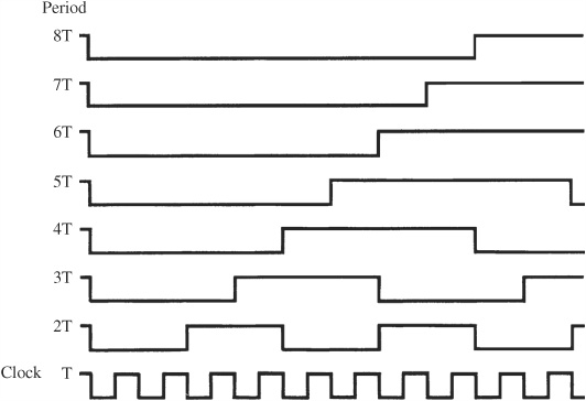
FIGURE 3.18 Run-length limited (RLL) codes regulate the number of transitions representing the channel code. In this way, transition spacings can be any multiple of the channel period, increasing data density.
As always, density must be balanced against other factors, such as clocking. Generally, d is selected to be as large as possible for high density, and k is selected to be as large as possible while maintaining stable clocking. Note that high k/d ratios can yield code sequences with high dc content; this is a shortcoming of RLL codes. The minimum and maximum lengths determine the minimum and maximum rates in the code waveform; by choosing specific lengths, the spectral response can be shaped.
RLL codes use a set of rules to convert information bits into a stream of channel bits by defining some relationship between them. A channel bit does not correspond to one information bit; the channel bits can be thought of as short timing windows, fractions of the clock period. Data density can be increased by increasing the number of possible transitions within a bit period. Channel bits are often converted into an output signal using NRZI modulation code; a transition defines a 1 in the channel bitstream. The channel bit rate is usually greater than the information bit rate, but if the run lengths between 1s can be distinguished, the overall information density can be increased. To ensure that consecutive codewords do not violate the run length and to ensure dc-free coding, alternate codewords or merging bits may be placed between codewords; however, this decreases density. Generally, RLL codes are viable only in channels with low noise; for example, the required S/N ratio increases as minimum length d increases. Fortunately, optical discs are suitable for RLL coding. Technically, NRZ and NRZI are RLL codes because d = 0 and k = ∞ MFM could be considered as a (1,3) RLL code.
In the group coded recording (GCR) code, data is parsed into four bits, coded into 5-bit words using a lookup table as shown in Table 3.1, and modulated as NRZI signals. This implementation is sometimes known as 4/5 MNRZI (modified NRZI) code. There is a transition every three bits, because of the 4/5 conversion, the minimum interval is 0.8T, and the maximum interval is 2.4T. Adjacent 1s are permitted (d = 0) and the maximum number of 0s is 2 (k = 2). The code is self-clocking with great immunity to jitter, but exhibits dc content. The density ratio is 0.8.
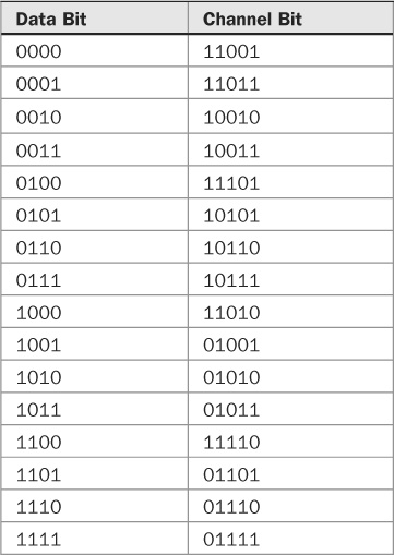
TABLE 3.1 Conversion for the GCR (or 4/5 MNRZI) code. Groups of four information bits are coded as 5-bit patterns, and written in NRZI form.
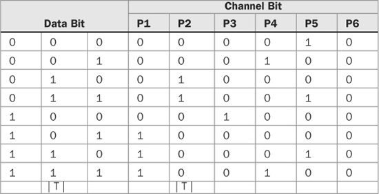
TABLE 3.2 Conversion for 3PM (2,7) code. Three input bits are coded into a 6-bit output word in which the minimum interval is maintained at 1.57 through pattern inversion.
The three-position modulation (3PM) code is a (2,7) RLL adaptive code. Three input bits are converted into a 6-bit output word in which Tmin is 1.5T and Tmax is 6T, as shown in Table 3.2. There must be at least two channel 0s between 1s (d = 2). When 3PM words are merged, a 101 pattern might occur; this violates the Tmin rule. To prevent this, 101 is replaced by 010; the last channel bit in the coding table is reserved for this merging operation. The 3PM code is so called because of the three positions (d + 1) in the minimum distance. The code is self-clocking. For comparison, the duration between transitions for 3PM is 0.5T and for MFM is T. Thus, the packing density of 3PM is 50% higher than MFM. However, its maximum transition is 100% longer and its jitter margin 50% worse. 3PM exhibits dc content. Data density is 1.5.
In the 4/5 group code, groups of four input bits are mapped into five channel bits using a lookup table. The 16 channel codewords are selected (from the 32 possible) to yield a useful clocking signal while minimizing dc content. Adjacent 1s are permitted (d = 0) and the maximum number of 0s is 3 (k = 3). Tmax = 16/5 = 3.2T. Density ratio is 0.8 and FoM is 0.64. The 4/5 code is used in the Fiber Distributed Data Interface (FDDI) transmission protocol, and the Multichannel Audio Digital Interface (MADI) protocol as described in Chap. 13.
As noted, RLL codes are efficient because the distance between transitions is changed in incremental steps. The effective minimum wavelength of the medium becomes the incremental run lengths. Part of this advantage is lost because it is necessary to avoid all data patterns that would put transitions closer together than the physical limit. Thus all data must be represented by defined patterns. The eight-to-fourteen modulation (EFM) code is an example of this kind of RLL pattern coding. The incremental length for EFM is one-third that of the minimum resolvable wavelength. Data density is not tripled, however, because 8 data bits must be expressed in a pattern requiring 14 incremental periods. To recover this data, a clock is run at the incremental period of 1T.
EFM code is used to store data on a Compact Disc; it is an efficient and highly structured (2,10) RLL code. Blocks of 8 data bits are translated into blocks of 14-bit channel symbols using a lookup table that assigns an arbitrary and unique word. The 1s in the output code are separated by at least two 0s (d = 2), but no more than ten 0s (k = 10). That is, Tmin is 3 channel bits and Tmax is 11 channel bits. A logical 1 causes a transition in the medium; this is physically represented as a pit edge on the CD surface. High recording density is achieved with EFM code. Three merging bits are used to concatenate 14-bit EFM words, so 17 incremental periods are required to store 8 data bits. This decreases overall information density, but creates other advantages in the code. Tmin is 1.41T and Tmax is 5.18T. The theoretical recording efficiency is thus calculated by multiplying the threefold density improvement by a factor of 8/17, giving 24/17, or a density ratio of 1.41. That is, 1.41 data bits can be recorded per shortest pit length. For practical reasons such as S/N ratio and timing jitter on clock regeneration, the ratio is closer to 1.25. In either case, there are more data bits recorded than are transitions on the medium. The merging bits completely eliminate dc content, but reduce efficiency by 6%. The conversion table was selected by a computer algorithm to optimize code performance. From a performance standpoint, EFM is very tolerant of imperfections, provides high density, and promotes stable clock recovery by a self-clocking decoder. EFM is used in the CD format and is discussed in Chap. 7. The EFMPlus code used in the DVD format is discussed in Chap. 8. The 1-7PP code used in the Blu-ray format is discussed in Chap. 9.
Zero modulation (ZM) coding is an RLL code with d = 1 and k = 3; it uses a convolutional scheme, rather than group coding. One information bit is mapped into two data bits, coded with rules that depend on the preceding and succeeding data patterns, and written in NRZI code. As with many RLL codes that followed it, ZM uses data patterns that are optimal for its application (magnetic recording) and were selected by computer search. Generally, the bitstream is considered as any number of 0s, two 0s separated by an odd number of 1s or no 1s, or two 0s separated by an even number of 1s. The first two types are coded as Miller code, and in the last, the 0s are coded as Miller code, but the 1s are coded as if they were 0s, but without alternate transitions. The density ratio is approximately 1. There is no dc content in ZM.
An eight-to-ten (8/10) modulation group code was selected for the DAT format in which 8-bit information words are converted to 10-bit channel words. The 8/10 code permits adjacent channel 1s, and there are no more than three channel 0s between 1s. The density ratio is 0.8, and FoM is 0.64. Bit synchronization and block synchronization are provided with a 3.2T + 3.2T synchronization signal, a prohibited 8/10 pattern. The ideal 8/10 codeword would have no net dc content, with equal durations at high and low amplitudes in its modulated waveform. However, there are an insufficient number of such 10-bit channel words to represent the 256 states needed to encode the 8-bit data input. Moreover, given the maximum run length limitation, only 153 channel codes satisfy both requirements. Thus 103 codewords must have dc content, or nonzero digital sum value (DSV). The DSV tallies the high-amplitude channel bit periods versus the low-amplitude channel bit periods as encoded with NRZI. Two patterns are defined for each of the 103 nonzero DSV codewords, one with a +2 DSV and one with a −2 DSV; to achieve this, the first channel bit is inverted. Either of these codewords can be selected based on the cumulative DSV. For example, if DSV ranges negatively, a +2 word is selected to tend toward a zero dc condition. Channel codewords are written to tape with NRZI modulation. The decoding process is relatively easy to implement because DSV need not be computed. Specifications for a number of simple and group codes are listed in Table 3.3.
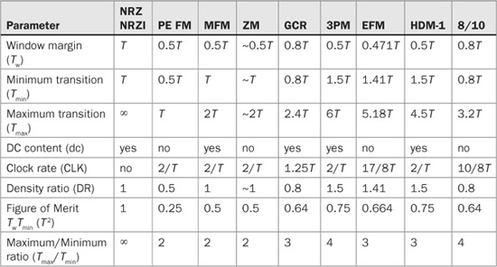
TABLE 3.3 Specification for a number of simple and group codes.
Code Applications
Despite different requirements, there is similarity of design between codes used in magnetic or optical recording. Practical differences between magnetic and optical recording codes are usually limited to differences designed to optimize the code for the specific application. Some codes such as 3PM were developed for magnetic recording, but later applied to optical recording. Still, most practical applications use different codes for either magnetic or optical recording.
Optical recording requires a code with high density. Run lengths can be long in optical media because clock regeneration is easily accomplished. The clock content in the data signal provides synchronization of the data, as well as motor control. Because this clock must be regenerated from the readout signal (for example, by detecting pit edges) the signal must have a sufficient number of transitions to support regeneration, and the maximum distance between transitions ideally must be as small as possible. In an optical disc, dirt and scratches on the disc surface change the envelope of the readout signal, creating low-frequency noise. This decreases the average level of the readout signal. If the signal falls below the detection level, it can cause an error in readout. This low-frequency noise can be attenuated with a highpass filter, but only if the information data itself contains no low-frequency components. A code without dc content thus improves immunity to surface contamination by allowing insertion of a filter. Compared to simple codes, RLL codes generally yield a larger bit-error rate because of error propagation; a small physical error can affect proportionally more bits. Still, RLL codes offer good performance in these areas and are suitable for optical disc recording. Ultimately, a detailed analysis is needed to determine the suitability of a code for a given application.
In many receiving circuits, a phase-locked loop (PLL) circuit is used to reclock the channel code, for example, from a storage medium. The channel code acts as the input reference, the loop compares the phase difference between the reference and its own output, and drives an internal voltage-controlled oscillator to the reference frequency, decoupling jitter from the signal. The comparison occurs at every channel transition, and interim oscillator periods count the channel periods, thus recovering the code. A synchronization code is often inserted in the channel code to lock the PLL. In an RLL code, a pattern violating the run length can be used for synchronization; for example, in the CD, two 11T patterns precede an EFM frame; the player can lock to the channel data, and will not misinterpret the synchronization patterns as data.
Following channel coding, the data is ready for storage or transmission. For example, in a hard-disk recorder, the data is applied to a recording circuit that generates the current necessary for saturation recording. The flux reversals recorded on the disk thus represent the bit transitions of the modulated data. The recorded patterns might appear highly distorted; this does not affect the integrity of the data, and permits higher recording densities. In optical systems such as the Compact Disc, the modulation code results in pits. Each pit edge represents a binary 1 channel bit, and spaces between represent binary 0s. In any event, storage to media, transmission, or other real-time digital audio processing, marks the end of the digital recording chain.