
CHAPTER 4
Digital Audio Reproduction
Digital audio recording and reproduction processors serve as input and output transducers to the digital domain. They convert an analog audio waveform into a signal suitable for digital processing, storage, or transmission, and then convert the signal back to analog form for playback. In a linear pulse-code modulation (PCM) system, the functions of the reproduction circuits are largely reversed from those in the record side. Reproduction functions include timebase correction, demodulation, demultiplexing, error correction, digital-to-analog (D/A) conversion, output sample-and-hold (S/H) circuit, and output lowpass filtering. Oversampling digital filters, preceding D/A conversion, are used universally.
Reproduction Processing
The reproduction signal chain accepts a coded binary signal and ultimately reconstructs an analog waveform, as shown in Fig. 4.1. The reproduction circuits must minimize any detrimental effects of data storage or transmission. For example, storage media suffer from limitations such as mechanical variations and potential for physical damage. With analog storage, problems generally must be corrected within the medium itself; for example, to minimize wow and flutter, a turntable’s speed must be precise. With digital systems, the potential for degradation is even greater. However, digital processing offers the opportunity to correct many faults. For example, the reproduction circuits buffer the data to minimize the effects of timing variations in the data, and also perform error correction.
To achieve high data density, the physical fidelity of the stored or transmitted channel code waveform is allowed to deteriorate. Thus, the signal does not have the clean characteristics that the original data may have enjoyed. For example, a recorded digital signal as read from a magnetic-disk head is not sharply delineated, but instead is noisy and rounded from bandlimiting. A waveform shaper circuit identifies the transitions and reconstructs a valid data signal. In this way, data can be recovered without penalty for the waveform’s deterioration.
Synchronization pulses and other clocking information in the bitstream are identified and used by timebase correction circuits to synchronize the playback signal, delineate individual frames, and thus determine the binary content of each pulse. In most cases, the signal contains timing errors such as jitter as it is received for playback. Phase-locked loops (PLLs) and data buffers can overcome this problem. A buffer can be thought of as a pail of water: water is poured into the pail carelessly, but a spigot at the bottom of the pail supplies a constant stream. Specifically, a buffer is a memory into which the data is fed irregularly, as it is received. However, data is clocked from the buffer at an accurately controlled rate, ensuring precise data timing. Samples can be reassembled at the same rate at which they were taken. Timebase correction is discussed in more detail later in this chapter.
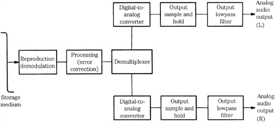
FIGURE 4.1 A conceptual linear PCM reproduction section. In practice, digital oversampling filters are used.
The modulated audio data, whether it is eight-to-fourteen modulation (EFM), modified frequency modulation (MFM), or another code, is typically demodulated to nonreturn to zero (NRZ) code, that is, a simple code in which the amplitude level represents the binary information. The audio data thus regains a readily readable form and is ready for further reproduction processing. In addition, demultiplexing is performed to restore parallel structure to the audio data. The demultiplexer circuit accepts a serial bit input, counting as the bits are clocked in. When a full word has been received, it outputs all the bits of the word simultaneously, to form parallel data.
The audio data and coded error-correction data are identified and separated from other peripheral data. Using the error-correction data, the data signal is checked for errors that may have occurred following encoding. Because of the data density used in digital recording and transmission, many systems anticipate errors with certainty; only their frequency and severity vary. The error-correction circuits must de-interleave the data. Prior to recording, the data is scattered in the bitstream to ensure that a defect does not affect consecutive data. With de-interleaving, the data is properly reassembled in time, and errors caused by intervening defects are scattered through the bitstream, where they are more easily corrected. The data is checked for errors using redundancy techniques. When calculated parity does not agree with parity read from the bitstream, an error has likely occurred in the audio data. Error correction algorithms are used to calculate and restore the correct values. If within tolerance, errors can be detected and corrected with absolute fidelity to the original data, making digital recording and transmission a highly reliable technique. If the errors are too extensive for correction, error concealment techniques are used. Most simply, the last data value is held until valid data resumes. Alternatively, interpolation methods calculate new data to form a bridge over the error. A more complete discussion of error correction techniques can be found in Chap. 5. The serial bitstream consists of the original audio data, or at least data as close to the original as the error correction circuitry has yielded. On leaving the reproduction processing circuitry, the data has regained timing stability, been demultiplexed, been de-interleaved, and incurred errors have been corrected. The data is ready for digital-to-analog conversion. Digital filtering, which precedes D/A conversion, is discussed later in this chapter.
Digital-to-Analog Converter
The digital-to-analog (D/A) converter is one of the most critical elements in the reproduction system. Just as the analog-to-digital (A/D) converter largely determines the overall quality of the encoded signal, the D/A converter determines how accurately the digitized signal will be restored to the analog domain. The task of D/A conversion demands great precision; for example, with a ±10-V scale, a 16-bit converter will output voltage steps that measure 0.000305 V, and a 24-bit converter must output steps that measure only 0.00000119 V. Traditional D/A converters can exhibit nonlinearity similar to that of A/D converters; sigma-delta converters, operating on a time basis rather than an amplitude basis, can overcome some deficiencies but must use noise shaping to reduce the in-band noise floor. Fortunately, high-quality D/A converters are available at low cost.
Traditional D/A converters process parallel data words and are prone to many of the same errors as A/D converters, as described in Chap. 3. In practice, resolution is chiefly determined by absolute linearity error and differential linearity error. Absolute linearity error is a deviation from the ideal quantization staircase and can be measured at full signal level; it is smaller than ±1/2 LSB (least significant bit). Differential linearity error is a relative deviation from the ideal staircase by any individual step. The error is uncorrelated with high signal levels but correlated with low signal levels; as a result it is most apparent at low signal levels as distortion.
Differential nonlinearity appears as wide and narrow codes, and can cause entire sections of the transfer function to be missing. Differential nonlinearity is minor with high-amplitude signals but the errors can dominate low-level signals. For example, a signal at −80 dBFS (dB Full Scale) will pass through only six or seven codes in a 16-bit quantizer; if half of those codes are missing, the result will be 14-bit performance. Depending on bias, the differential linearity error in a 16-bit D/A converter for a −90 dBFS sine wave signal can result in generated levels ranging from −85.9 dB to −98.2 dB. Because the bits and their associated errors switch in and out throughout the transfer function, their effect is signal dependent. Thus, harmonic and intermodulation distortion and noise vary with signal conditions. Because this kind of error is correlated with the audio signal, it is more readily perceived. Nonmonotonicity is an extreme case of nonlinearity; an increase in a particular digital code does not result in an increase in the output analog voltage; most converters are guaranteed against this.
A linearity test measures the converter’s ability to record or reproduce various signals at the proper amplitude. Specifically, linearity describes the converter’s ability to output an analog signal that directly conforms to a digital word. For example, when a bit changes from 1 to 0 in a D/A converter, the analog output must decrease exactly by a proportional amount. Any nonlinearity results in distortion in the audio signal; the amount that the analog voltage changes will depend on which bit has changed. Every PCM digital word contains a series of binary digits, arranged in powers of two. The most significant bit (MSB) accounts for a change in fully half of the analog signal’s amplitude, and the least significant bit accounts for the least change, for example, in an 18-bit word, an amplitude change of less than four parts per million. Physical realities conspire against this accuracy. Traditional ladder converters exhibit differential nonlinearity because of bit weighting errors; thermal or physical stress, aging, and temperature variations are also factors.
To help equipment manufacturers use D/A converters to their best advantage, some ladder D/A chips provide a means to calibrate the converter. Consider a 16-bit D/A converter offering calibration of the MSB. Because the MSB is so much larger than the other bits, an MSB error of only 0.01% (one part in 10,000) would completely negate the contributions of the two LSBs (which account for one part in 21,845 of the total signal amplitude). An error of 0.1% in the MSB would swamp the combined values of the five smallest bits. Overall, the tolerance of the MSB in a 16-bit converter is 1/65,536 of the LSB. Some converters offer calibration of the four most significant bits. It is interesting to note that fully 93% of the total analog output is represented through these four most significant bits. These MSBs largely steer the converter’s output amplitude; when they are properly calibrated, the entire output signal of a well-designed D/A converter will be more accurate. This accuracy is most significant at low levels, usually below −60 dBFS. As noted, any nonlinearity in D/A conversion will be apparent as a deviation from nominal amplitude. Moreover, such nonlinearity can be heard; for example, by using a test disc containing a dithered fade to silence tone, poor D/A linearity is clearly audible.
The low-level performance of D/A converters can be evaluated using tests for D/A linearity. For example, Fig. 4.2 shows a D/A converter’s low-level linearity. Reproduced signals lower than −100 dBFS in amplitude show nonlinearity. For example, a −100-dBFS signal is reproduced at an amplitude of −99 dBFS, and a −110-dBFS signal is reproduced at approximately −105 dBFS. Depending on signal conditions, this kind of error in low-level dynamics might audibly alter low-amplitude information.
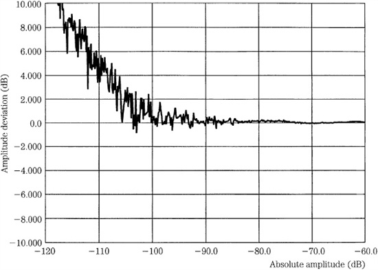
FIGURE 4.2 An example of a low-level linearity measurement of a D/A converter showing increasing nonlinearity with decreasing amplitude.
In practice, linear 16-bit conversion is insufficient for 16-bit data. Converters must have a greater dynamic range than the audio signal itself. No matter how many bits are converted, the accuracy of the conversion, and hence the fidelity of the audio signal, hinges on the linearity of the converter. Linearity errors in converters generally result in a stochastic deviation; it varies randomly from sample to sample. However, relative error increases as level decreases. The linearity of a D/A converter, and not the number of bits it uses, measures its accuracy.
A D/A converter must have a fast settling time. Settling time for a D/A converter is the elapsed time between a new input code and the time when the analog output falls within a specified tolerance (perhaps ±1/2 LSB). The settling time can vary with the magnitude of change in the input word.
Most D/A converters operate with a two’s complement input. For example, an 8-bit D/A converter would have a most positive value of 01111111 and a most negative value of 10000000. In this format the MSB is complemented to serve as a sign bit. To accomplish this, the MSB can be inverted before the word is input to the D/A converter, or the D/A converter might have a separate, complementing input for the MSB.
Digitally generated test tones are often used to measure D/A converters; it is important to choose test frequencies that are not correlated with the sampling frequency. Otherwise, a small sequence of codes might be reproduced over and over, without fully exercising the converter. Depending on the converter’s linearity at those particular codes, the output distortion might measure better, or worse, than typical performance. For example, when replaying a 1-second, 1-kHz, 0-dBFS sine wave sampled at 44.1 kHz, only 441 different codes would be used over the 44,100 points. A 0-dBFS sine wave at 997 Hz would use 20,542 codes, giving a much better representation of converter performance. Standard test tones have been selected to avoid this anomaly. For example, some standard test frequencies are: 17, 31, 61, 127, 251, 499, 997, 1999, 4001, 7993, 10,007, 12,503, 16,001, 17,989, and 19,997 Hz.
Weighted-Resistor Digital-to-Analog Converter
Various types of D/A converters are used for audio digitization. Operation of traditional converters is quite different from sigma-delta converters. The former are more easily understood; we begin with an illustration of the operation of a traditional ladder D/A converter. A D/A converter accepts an input digital word and converts it to an output analog voltage or current. The simplest kind of D/A converter, known as a weighted-resistor D/A converter, contains a series of resistors and switches, as shown in Fig. 4.3.
A weighted-resistor converter contains a switch for each input bit; the corresponding resistor represents the binary value associated with that bit. A reference voltage generates current through the resistors. A digital 1 closes a switch and contributes a current, and a digital 0 opens a switch and prevents current flow. An operational amplifier sums the currents and converts them to an output voltage. A low-value binary word with many 0s closes few switches thus a small voltage results. A high-value word with many 1s closes many switches; thus, a high voltage results. Consider this example of an 8-bit converter:
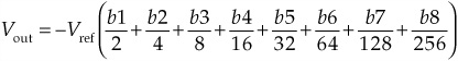
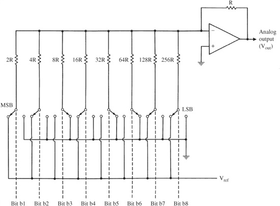
FIGURE 4.3 A weighted-resistor D/A converter uses resistors related by powers of 2, which limits resolution.
where b1 through b8 represent the input binary bits. For example, suppose the reference voltage Vref = 10 V and the input word is 11010011:
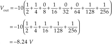
Although this weighted-resistor design looks good on paper, it is rarely used in practice because of the complexity in manufacturing resistors with sufficient accuracy. It is extremely difficult to manufacture precise resistor values so that each next resistor value is exactly a power of 2 greater than the previous one. For example, in a 16-bit D/A converter, the largest-to-smallest ohm (Ω) resistor ratio is 65,536:1. If the smallest resistor value is 1 kΩ, the largest is over 65 MΩ. Similarly, the smallest current might be 30 nA (nanoampere) and the largest 2 mA (milliampere). In short, this design demands manufacturing conditions that cannot be efficiently met.
R-2R Ladder Digital-to-Analog Converter
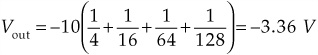
A more suitable design approach for a D/A converter is the R-2R resistor ladder, as shown in Fig. 4.4. This circuit contains resistors and switches; in particular, there are two resistors per bit. Each switch contributes its appropriately weighted component to the output. The current splits at each node of the ladder, resulting in current flows through the switch resistors that are weighted by binary powers of 2. If current I flows from the reference voltage, I/2 flows through the first switch, I/4 through the second switch, I/8 through the third switch, and so on. Digital input bits are used to control ladder switches to produce an analog output. For example:
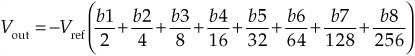
With Vref = 10 V and an input word of 01010110:
The R-2R network can be efficiently manufactured; only two values of resistors are needed. As noted, in many converters, one or several MSBs can be calibrated to improve linearity. In some designs, stability with respect to temperature is achieved with a compensation feedback loop. A high-precision signal is generated and compared to the signal generated by the D/A converter. The difference between the two is applied to a memory, which in turn outputs a correction word to the input of the D/A converter. Errors caused by variations in the components are thus self-corrected and distortion is minimized.
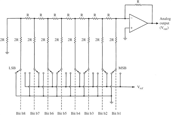
FIGURE 4.4 An R-2R D/A converter uses only two resistor values, improving resolution.
Zero-Cross Distortion
A quality D/A converter must be highly accurate. As noted, a 16-bit D/A converter with an output range of ±10 V has a difference between quantization levels of 20/65,536 = 0.000305 V. For example, the output from the input word 1000 0000 0000 0000 should be 0.3 mV larger than that from the input word 0111 1111 1111 1111. In other words, the sum of the lower 15 bits must be accurate to that precision, compared to the value of the highest bit. The lower 15 bits should have a relative error of one-half quantization level, as should the MSB. However, differential linearity error is greatest for the MSB, which produces the largest output voltage. Moreover, the MSB changes each time the output waveform passes through zero. Difficulty in achieving accuracy at the center of a ladder D/A converter’s range leads to zero-cross distortion.
Zero-cross distortion occurs at the zero-cross point between the positive and negative polarity portions of an analog waveform. When a resistor ladder D/A converter is switched around its MSB, that is, from 1000 0000 0000 0000 to 0111 1111 1111 1111 to reflect a polarity change, the internal network of resistors must be switched. Current fluctuations and variations in bit switching speeds can conspire to create differential nonlinearity and glitches, as shown in Fig. 4.5. Collectively, these defects are known as zero-cross distortion. Because musical waveforms continually change (twice each cycle) between positive and negative polarity, the zero axis is crossed repeatedly as the MSB is turned on and off. The error is particularly troublesome when reproducing low-level signals because the fixed-amplitude glitch may be proportionally large with respect to the signal. Furthermore, the audibility of zero-cross distortion can be aggravated by dithering because of the increase in the number of transitions around the MSB.
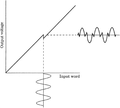
FIGURE 4.5 Crossover distortion occurs at the zero-cross point when the input word of a D/A converter changes polarity, resulting in a glitch in the output waveform.
Ideally, when there is no error difference between the smallest and largest resistors in the ladder, there is no output error. However, the MSB generally has large error compared to the LSB; the error can be larger than the value of the LSB itself. This is because the MSB in a 16-bit converter must be represented by a current value with an accuracy greater than 1/65,536 of the LSB. (This demonstrates why adjustment of the MSB is paramount in achieving converter linearity.) Similarly, error can occur when the 2nd, 3rd, and 4th bits are switched; however, the error proportionally decreases as the signal level increases. By the same token, error is relatively greatest for low-level audio signals. When longer word-length converters are used, it is proportionally difficult to match resistor values.
Zero-cross distortion can be alleviated by careful calibration of the converter’s most significant bits. Alternatively, a sign-magnitude configuration can be used; the output amplifier switches between each positive and negative input code excursion. As a result, the LSB toggles around bipolar-zero, minimizing zero-cross distortion. Zero-cross distortion can also be reduced by providing a complementary D/A converter for each waveform polarity. Sign-magnitude code values are supplied to both parallel converters. In this way, total switching of digits across bipolar-zero never occurs. Zero-cross distortion is not present in sigma-delta D/A converters, as described in Chap. 18.
High-Bit D/A Conversion
Many manufacturers use D/A converters with 18-, 20- or 24-bit resolution in reproduction systems to provide greater playback fidelity for 16-bit recordings. The rationale for this lies in flaws that are inherent in D/A converters. Except in theory, 16-bit converters cannot fully decode a 16-bit signal without a degree of error. When, for example, 18 bits are derived from 16-bit data and converted with 18-bit resolution, errors can be reduced and reproduction specifications improved. To realize the full potential of audio fidelity, the signal digitization and processing steps must have a greater dynamic range than the final recording.
The choice of 16-bit words for the CD and other formats was determined primarily by the availability of 16-bit D/A converters and the fact that longer word lengths diminish playing time. However, 18-bit converters, for example, can provide better conversion of the stored 16 bits. When done correctly, 18-bit conversion improves amplitude resolution by ensuring a fully linear conversion of the 16-bit signal. An 18-bit D/A converter has 262,144 levels, exactly four times as many output levels as a 16-bit converter. Any nonlinearity is correspondingly smaller, and increasing the quantization word length at the conversion stage results in an increase in signal-to-noise (S/N) ratio. Simultaneously, any quantization artifacts are diminished. In other words, in this example, an 18-bit D/A converter gives better 16-bit conversion. In fact, the two extra bits of a linear 18-bit converter do not have to be connected to yield improved 16-bit performance.
The intent of high-bit D/A converters can be compared to that of oversampling: while the sampling frequency is increased, the method does not create new information; it makes better use of existing information. Oversampling provides the opportunity for high-bit conversion of 16-bit data. When a 44.1-kHz, 16-bit signal is oversampled, both the sampling frequency and number of bits are increased—the former because of oversampling, and the latter because of filter coefficient multiplication. The digital filter must be appropriately designed so the output word contains useful information in the bits below the 16-bit level.
It is not meaningful to gauge the performance of a D/A or A/D converter by its word length. More accurately, the S/N ratio measures the ratio between the maximum signal and the noise in the absence of signal. Because systems mute the output when there is a null signal, low-level error is removed. A dynamic range measurement is more useful when measured as the ratio of the maximum signal to the broadband noise (0 Hz to 20 kHz) using a −60-dBFS signal. This provides a measure of low-level distortion. Using the dynamic range measurement, a converter’s ENOB (effective number of bits) can be calculated:
![]()
For example, a 16-bit converter with a dynamic range of 90 dB provides 14.7 bits of resolution; 1.3 bits are mired in distortion and noise.
In many designs, sigma-delta D/A converters are used. They minimize many problems inherent in traditional converter design. Sigma-delta systems use very high over-sampling rates, noise shaping, and one- or multi-bit conversion. A true one-bit system outputs a binary waveform, at a very high rate, to represent the audio waveform. Other multi-bit systems output a multi-value step signal that forms a pulse-width modulation (PWM) representation of the audio signal. Because of inherently high noise levels, sigma-delta systems must use noise-shaping algorithms. Sigma-delta conversion is discussed in Chap. 18.
Although sigma-delta converters are widely used, traditional converters can offer some advantages. Because traditional converters do not employ noise shaping, they do not yield high out-of-band noise. In addition, at very low signal levels, the binary-weighted current sources are not heavily switched, so noise and glitching artifacts are very low.
Output Sample-and-Hold Circuit
Many digital audio systems contain two sample-and-hold (S/H) circuits. One S/H circuit at the input samples the analog value and maintains it while A/D conversion occurs. Another S/H circuit on the output samples and holds the signal output from the D/A converter, primarily to remove irregular signals called switching glitches. Because it can also compensate for a frequency response anomaly called aperture error, the output S/H circuit is sometimes called the aperture circuit.
Many D/A converters can generate erroneous signals, or glitches, which are superimposed on the analog output voltage. Digital data input to a D/A converter may require time to stabilize to the correct binary levels. In particular, in some converters, input bits might not switch states simultaneously. For example, during an input switch from 01111111 to 10000000, the MSB might switch to 1 before the other bits; this yields a momentary value of 11111111, creating an output voltage spike of one-half full scale. Even D/A converters with very fast settling times can exhibit momentary glitches. If these glitches are allowed to proceed to the digitization system’s output, they are manifested as distortion.
An output S/H circuit can be used to deglitch a D/A converter’s output signal. The output S/H circuit acquires voltage from the D/A converter only when that circuit has reached a stable output condition. That correct voltage is held by the S/H circuit during the intervals when the D/A converter switches between samples. This ensures a glitch-free output pulse-amplitude modulation (PAM) signal. The operation of an output S/H circuit is shown in Fig. 4.6.

FIGURE 4.6 An output S/H circuit can be used to remove glitches in the signal output from some D/A converters.
From a general hardware standpoint, the output S/H circuit is designed similarly to the input S/H circuit. In some specifications, such as droop, the output S/H circuit might be less precise. Any droop results in only a dc shift at the digitization system’s output, and this can be easily removed. In other respects, the output S/H circuit must be carefully designed and implemented. Because of its differing utility, the output S/H circuit requires attention to specifications such as hold time and transition speed from sample to sample.
The S/H circuit is occasionally used to correct for aperture error, an attenuation of high frequencies. Different approaches can also be used. Aperture error stems from the width of the output samples. In this case, the narrower the pulse width, the less the aperture error. Given ideal (instantaneous) A/D sampling, the output of an ideal D/A converter would be an impulse train corresponding to the original sample points; there would be no high-frequency attenuation. However, an ideal D/A converter is an impossibility. The PAM staircase waveform comprises pulses each with a width of one sample period. (Mathematically, the function is a convolution of the original samples by a square pulse with width of one sample period.) The spectrum of a series of pulses of finite width naturally attenuates at high frequencies. This differs from the original flat response of infinitesimal pulse widths; thus, a frequency response error called aperture error results, in which high audio frequencies are attenuated. Specifically, the frequency response follows a lowpass sin(x)/x function. When the output pulse width is equal to the sample period, the frequency response is zero at multiples of the sampling frequency, as shown in Fig. 4.7A. The attenuation of the in-band high-frequency response and that of high-frequency images can be observed.
At the Nyquist frequency, the function’s value is 0.64, yielding an attenuation of 3.9 dB. This can be addressed with S/H circuits by approximating the impulse train output from an ideal D/A converter; the duration of the hold time is decreased in the S/H circuit. Sampling theory demonstrates that the bandwidth of the response is determined by the pulse width. The shorter the duration of the pulse, the greater the bandwidth. Specifically, if the output pulse width is narrowed with a shorter hold time, the attenuation at the half-sampling frequency can be decreased, as shown in Fig. 4.7B, where the pulse width is halved. If hold time is set to one-quarter of a sample period, the amplitude at the Nyquist frequency is 0.97, yielding an attenuation of 0.2 dB. This is considered optimal because a shorter hold time degrades the S/N ratio of the system.
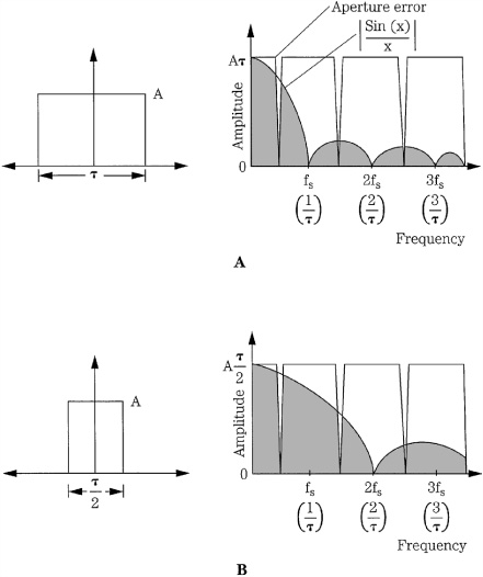
FIGURE 4.7 Aperture error can be minimized by decreasing the output pulse width. A. A pulse width equal to the sample period yields an in-band high-frequency attenuation. B. In-band high-frequency response improves when pulse width is one-half the sample period.
Another remedy for aperture error is frequency compensation of the data prior to D/A conversion; this can be built into the digital lowpass filter that precedes the S/H circuit. This high-frequency boost, offset by aperture error, produces a net flat response, and the S/N ratio is not degraded. A boost could also be designed into the succeeding analog lowpass filter. Alternatively, a pre-emphasis high-frequency boost could be applied at the system input; the naturally occurring de-emphasis at the output S/H circuit would result in a flat response.
When an output S/H circuit is used to eliminate switching errors caused by the D/A converter during transition, the S/H circuit must avoid introducing transition errors of its own. An S/H circuit outputs a steady value while in the hold mode. When switching to the sample (or acquisition) mode, a slow transition introduces incorrect intermediate values into the staircase voltage. This problem is extraneous in the input S/H circuit because the A/D converter accomplishes its digitization during the hold mode and ignores the transition mode. However, the output S/H circuit is always connected to the system output and any transition error appears at the output. In other words, not only are the levels themselves part of the output signal, but the way in which the S/H circuit moves from sample to sample is included as well.
Distortion is greatest for high frequencies because they have a large difference between values. For example, with a 48-kHz sampling frequency, a 20-Hz signal does not change appreciably in one sampling interval; however, a high-level 20-kHz signal will traverse almost the full amplitude range. Although the distortion products themselves can be removed by the output filter, these products can internally beat with the sampling frequency to generate in-band distortion as well. To overcome this problem, the output S/H circuit must switch as quickly as possible from hold to sample mode. A square-wave response would be ideal.
In theory, this eliminates the possibility of distortion caused by transition; however, in practice, it is impossible to achieve the necessary high slew rate, calculated to be as high as 5 V/ns (volts per nanosecond). Thus, an additional modification to the basic S/H circuit can be applied. An exponential change in amplitude from one quantization interval to the next does not create nonlinearity in the signal. Following output filtering, this exponential acquisition results in a linear response. It can be shown that an exponential transition from sample to sample causes only a slight high-frequency de-emphasis at the output, but no distortion or nonlinearity. An S/H circuit that integrates the difference between its present and next value yields such an exponential transition. The attenuation of high frequencies in an integrate-and-hold circuit is less than that produced by the sample-and-hold process itself, and also can be equalized.
The output S/H circuit thus removes switching glitches from the D/A converter’s output voltage. Hold time can be set to less than a sample period to minimize aperture error. Many D/A converters are stringently designed to avoid switching glitches, and thus operate without an S/H circuit; aperture error is corrected in the digital filter. In some cases, the S/H function is included in the D/A converter chip. Whichever method is used, the PAM staircase analog signal is ready for output filtering, and final reconstruction.
Output Lowpass Filter
The first and last circuits in an audio digitization system are lowpass filters, known as anti-aliasing and anti-imaging filters, respectively. Although their analog designs can be almost identical, their functions are very different. In lieu of classic analog anti-imaging filters, digital filters using oversampling techniques have replaced brick-wall analog filters. However, even digital filters employ a low-order analog lowpass filter on the final output of the system.
Given the criteria of the Nyquist sampling theorem, the function of the input low-pass filter is clear: it removes all frequency content above the half-sampling frequency to prevent aliasing. Similarly, a lowpass filter at the output of the digitization system removes frequency content above the half-sampling frequency. However, its function is different. This filter converts the D/A converter’s output pulse-amplitude modulation (PAM) staircase to a smoothly continuous waveform, thus reconstructing the bandlimited input signal. The PAM staircase is an analog waveform, but it contains modulation artifacts of the sampling process that create high-frequency components not present in the original signal. An output lowpass filter converts the staircase into a smoothly continuous waveform by removing the high-frequency components, leaving the original waveform. The staircase signal is smoothed; the output filter is sometimes called a smoothing filter.
The conceptual design criteria for an analog output lowpass filter are similar to those of the input filter. The passband should be flat and the stopband highly attenuated. The cutoff slope should be steep. Audibility of any phase shift must be considered. One criteria unique to output lowpass filters is transient response. Unlike the input filter, it must process the amplitude changes in the staircase waveform. Just as a slow output S/H circuit can introduce distortion, the output filter can create unwanted byproducts if its transient response is inadequate. One consideration not commonly addressed is the possible presence of extreme high-frequency components of several megahertz that might be contained in the output signal. Because of its high-speed operation, digital processing equipment can create this noise, and the filtering characteristics of some audio lowpass filters do not extend to those frequencies.
Viewing the output filtering process from a more mathematical standpoint, we can observe how sampling creates the need for filtering. Sampling multiplies the time domain audio signal with the time domain sampling (pulse) signal. In terms of the spectra of these two sampled signals, this convolution produces a new sampled spectrum identical to the original unsampled spectrum. However, additional spectra are infinitely repeated across the frequency domain at multiples of the sample frequency. For example, an original 1-kHz sine wave sampled at 48 kHz also creates components at 47, 49, 95, 97 kHz, and so on. Although the sample-and-hold process substantially reduces the amplitude of the extraneous frequency bands, significant components still remain after the S/H circuit, particularly in the region near the audio band (see Fig. 4.7). To convert the sampled information back into correct analog information, the image spectra must be removed, leaving only the original baseband spectrum. This is accomplished by output lowpass filtering.
Some might question the need to filter out frequencies above the Nyquist frequency because they lie above the presumed limit of human audibility. The original waveform is reproduced without filtering, but filtering is needed because the accompanying spectra could cause modulation in other downstream equipment through which the signal passes. This in turn could negatively affect the audio signal. Other digital systems might be immune because their input filters remove the high frequencies, but oscillators in analog recorders or transmitters could conceivably create difference frequencies in the audible band. Clearly, in systems with lower sampling frequencies (e.g., 8 kHz) any images above the Nyquist frequency would be audible, and thus must be removed.
Impulse Response
Logically, when an impulse is input to a device such as a lowpass filter, the output is the filter’s impulse response. As explained in Chap. 17, the impulse response can completely characterize a system: a filter can be described by its time-domain impulse response or its frequency response; these are related by the Fourier transform. Furthermore, multiplying an input spectrum by a desired filter transfer function in the frequency domain is equivalent to convolving the input time-domain function with the desired filter’s impulse response in the time domain. An ideal lowpass filter with a brick-wall response in the frequency domain, shown in Fig. 4.8A, displays an impulse response in the time domain that takes the form of sin(x)/x, as shown in Fig. 4.8B. The sin(x)/x function is also known as the sinc function. As we will see, this is an important key to understanding how a digital audio system can reconstruct the output waveform.
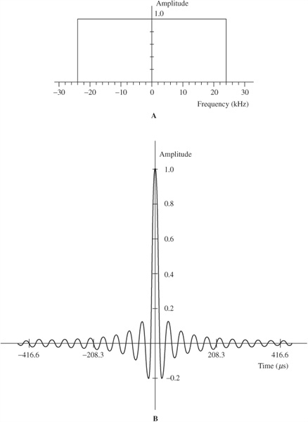
FIGURE 4.8 An impulse response completely characterizes a system. A. The frequency response of an ideal brick-wall lowpass filter with a 24-kHz cutoff frequency. B. The time-domain impulse response of the ideal brick-wall filter shown above. The sin(x)/x function passes through 0 at multiples of the sampling period of 1/48,000 Hz. The ringing thus occurs at 24 kHz.
The action of lowpass filtering, and the impulse response, is summarized in Fig. 4.9. In this example, the input signal comprises two sine waves of different frequencies Fig. 4.9A); their spectra consist of two lines at the sine wave frequencies (Fig. 4.9B). Suppose that we wish to lowpass filter the signal to remove the higher frequency. This is accomplished by multiplying the input spectra with an ideal lowpass filter characteristic (Fig. 4.9D), producing the single spectral line (Fig. 4.9F). The time-domain impulse response of this ideal lowpass filter follows a sin(x)/x function (Fig. 4.9C); if the input time-domain signal is convolved with the sin(x)/x function, the result is the filtered output time-domain signal (Fig. 4.9E). In other words, a time-domain, sampled signal can be filtered by applying the time-domain impulse response that describes the filter’s characteristic. In digital systems, both the signal and the impulse response are represented by discrete values; the impulse response of an ideal reconstruction filter is zero at all sample times, except at one central point.
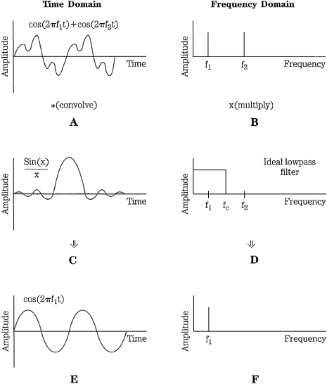
FIGURE 4.9 An example of lowpass filtering shown in the time domain (left column) and the frequency domain (right column). A. The input signal comprises two sine waves. B. Spectrum of the input signal. C. Impulse response of the desired lowpass filter is a sin(x)/x function. D. Desired lowpass filter transfer function. E. Output filtered signal is the convolution of the input with the impulse response. F. Spectrum of the output filtered signal is the multiplication of the input by the transfer function.
An ideal brick-wall output filter reconstructs the audio waveform. Although the idea of smoothing the output samples to remove high frequencies is essentially correct, a more analytical analysis shows exactly how waveform reconstruction is accomplished by lowpass filtering. An ideal brick-wall lowpass filter is needed to exactly reconstruct the output waveform from samples; the sampling theorem dictates this. As noted, an ideal brick-wall lowpass filter has a sin(x)/x impulse response. When samples of a bandlimited input signal are processed (convolved) with a sin(x)/x function, the band-limited input signal represented by the samples will be exactly reproduced; the sampling theorem guarantees this.
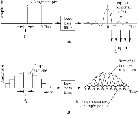
FIGURE 4.10 The impulse response of an ideal lowpass filter reconstructs the output analog waveform. A. The impulse response of an ideal lowpass filter is a sin(x)/x function; it is truncated in this drawing. B. When a series of impulses (samples) are lowpass-filtered, the individual impulse responses sum to form the output waveform.
Specifically, as shown in Fig. 4.10A, when a single rectangular audio sample passes through an ideal lowpass filter, after a filter delay it emerges with a sin(x)/x response. If the lowpass filter has a cutoff frequency at the half-sampling point (fs/2) then the sin(x)/x curve passes through zero at multiples of 1/fs. When a series of audio samples pass through the filter, the resulting waveform is the delayed summation of all the individual sin(x)/x contributions of the individual samples, as shown in Fig. 4.10B. Each sample’s impulse response is zero at the 1/fs position of any other sample’s maximum response. The output waveform has the value of each sample at sample time, and the summed response of the impulse responses of all samples between sample times. This superposition, or summation, of individual impulse responses forms all the intermediate parts of the continuous reconstructed waveform. In other words, when the high-frequency staircase components are removed, the remaining fundamental passes exactly through the same points as the original filtered waveform.
Output filtering, with an ideal lowpass filter, yields an output audio waveform that is theoretically identical to the input bandlimited audio waveform. In other words, it is the filter’s impulse response to the audio samples that reconstructs the original audio waveform. To summarize mathematically, we see that an ideal brick-wall filter outputs a sin(x)/x function at each sample time; moreover, the amplitude of each of these functions corresponds to the amplitude of the sample; when all the sin(x)/x functions are summed, the audio waveform is reconstructed.
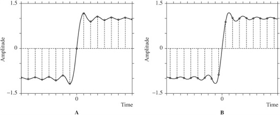
FIGURE 4.11 An audio signal is correctly reconstructed regardless of the sample location relative to the waveform timing. A. A bandlimited step is sampled with a sample at a zero-crossing time. B. A bandlimited step is sampled with samples symmetrical about the zero-crossing time. In these cases, and in other cases where samples occur at other times, the same waveform is reconstructed. (Lipshitz and Vanderkooy, 2004)
To return to a question posed in Chap. 2, we can again ask whether samples can capture waveform information that occurs between samples. The impulse response shows that they do. Moreover, the capture is successful no matter where the samples occur in relation to the waveform’s timing. Stanley Lipshitz and John Vanderkooy have concisely illustrated this. In Fig. 4.11A, a sample happens to fall exactly at the zero-crossing of a step waveform. The bandlimited step waveform (the heavy line) is reproduced (by the summed sin(x)/x functions). In Fig. 4.11B, samples fall at either side of the zero-crossing. Again, the waveform (heavy line) is exactly reconstructed. Similarly, the same waveform would be reconstructed no matter where the samples lie, and the zero-crossing time is the same. Also, nonintuitively, a higher sampling frequency does not somehow improve the resolution of the successful capture and reconstruction of this bandlimited waveform.
Digital Filters
Because of the phase shift and distortion they introduce, analog brick-wall output filters have been abandoned by manufacturers, in favor of digital filters. A digital filter is a circuit (or algorithm) that accepts audio samples and outputs audio samples; the values of the throughput audio samples are altered to produce filtering. When used on the output of a digital audio system, the digital filter simulates the process of ideal lowpass filtering and thus provides waveform reconstruction. Rather than suppress high-frequency images after the signal has been converted to analog form, digital filters perform the same function in the digital domain, prior to D/A conversion. Following D/A conversion, a gentle, low-order analog filter removes remaining images that are present at very high frequencies. In most cases, finite impulse response (FIR) digital filters are used; oversampling techniques allow a less complex digital filter design. With oversampling, additional sample values are computed by interpolating between original samples. Because additional samples are generated (perhaps two, four, or eight times as many), the sampling frequency of the output signal is greater than the input signal. A transversal filter architecture is typically used; it comprises a series of delays, multipliers, and adders.
The task of an oversampling filter is twofold: to resample, and to filter through interpolation. The signal input to the filter is sampled at fs, and has images centered around multiples of fs, as shown in Figs. 4.12A and B. Resampling begins by increasing the sampling frequency. That is accomplished by injecting zero-valued samples between original samples at some interpolation ratio. For example, for four-times oversampling, three zero-valued samples are inserted for every original sample as shown in Fig. 4.12C. The oversampling sampling frequency equals the interpolation ratio times the input sampling frequency, but the spectrum of the oversampled signal is the same as the original signal spectrum, as shown in Fig. 4.12D. In this case, for example, with an input sampling frequency of 48 kHz, the oversampling frequency is 192 kHz. This data enters the lowpass digital filter with a cutoff frequency of fs/2, operating at an effective frequency of 192 kHz. Although the original data was sampled at 48 kHz, with oversampling it is conceptually indistinguishable from data originally sampled at 192 kHz. The zero-packed signal is passed through a digital lowpass filter with the time-domain impulse response shown in Fig. 4.12E. The low-pass filter’s frequency-domain transfer function is shown in Fig. 4.12F. The fixed sample values in Fig. 4.12E, occurring at the oversampling frequency, comprise the coefficients of the digital transversal lowpass filter. The input (oversampled) samples convolved with the impulse response coefficients yield the filter’s output. In particular, the filter’s output is an interpolated digital signal, as shown in Fig. 4.12G, with images centered around multiples of the higher oversampling frequency fa, as shown in Fig. 4.12H.
To recapitulate, interpolation is used to create the intermediate sample points. In a four-times oversampling filter, the filter outputs four samples for every original sample. However, to be useful, these samples must be computed according to a certain algorithm. Specifically, each intermediate sample is multiplied by the appropriate sin(x)/x coefficient corresponding to its contribution to the overall impulse response of the lowpass filter in the time domain (see Fig. 4.10B). The sin(x)/x function in the time domain has zeros exactly aligned with sample times, except at the sample currently being interpolated. Thus, every interpolated sample is a linear combination of all other input samples, weighted by the sin(x)/x function. The multiplication products are summed together to produce the output-filtered sample. The conceptual operation of a digital filter thus corresponds exactly to the summed impulse response operation of an ideal analog brick-wall filter. Spectral images appear at multiples of the oversampled sampling frequency. Because the distance between the baseband and sidebands is larger, a gentle low-order analog filter can remove the images without causing a phase shift or other artifacts.
The oversampling ratio can be defined as
![]()
where fa = the oversampling frequency and fs = the input sampling frequency.
Oversampling initially requires insertion of (R − 1) zero samples per input sample. The samples created by oversampling must be placed symmetrically between the input samples. A lowpass filter is used to bandlimit the input data to fs/2, with spectral images at integer multiples of (R × fs). Moreover, lowpass filtering creates the intermediate sample values through interpolation. Rather than perform multiplication on zero samples, redundancy can be used advantageously to design a more efficient filter.
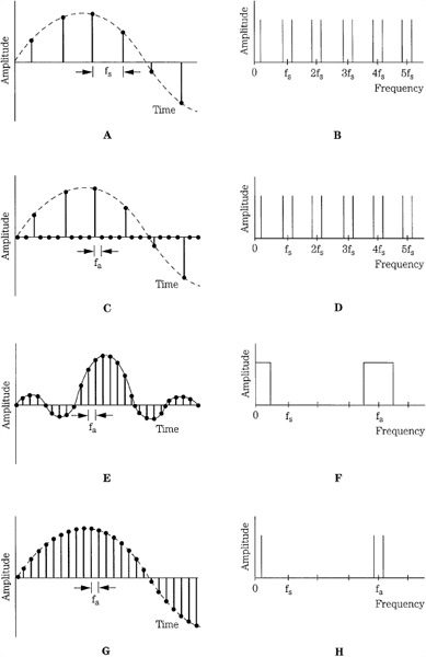
FIGURE 4.12 An oversampling filter resamples and interpolates the signal, using the impulse response; this is shown in the time domain (left column) and frequency domain (right column). A. The input signal is sampled at fs. B. The signal spectrum has images centered around multiples of fs. C. With resampling, zero-valued samples are placed between original samples at some interpolation ratio. D. The spectrum of the oversampled signal is the same as the original signal spectrum. E. The values of a sampled impulse response correspond to the coefficients of the digital filter. F. The transfer function of the filter shows passbands in the audio band and oversampling band. G. The digital filter performs interpolation to form new output sample values. H. The output-filtered signal has images centered around multiples of the oversampling frequency, fa.
FIR Oversampling Filter
As we have seen, a digital filter can use an impulse response as the basis of the computation to filter the audio signal. When the impulse response uses a finite number of points, the filter is called a finite impulse response (FIR) filter. In addition, in the case of an output lowpass filter, oversampling is used to extend the Nyquist frequency.
Figure 4.13 shows a four-times oversampling FIR digital filter, generating three intermediate samples between each input sample. The filter consists of a shift register of 24 delay elements, each delaying a 16-bit sample for one input sampling period. Thus each sample remains in each delay element for a sample period before it shifts to the next delay element. During this time each 16-bit sample is tapped off the delay line and multiplied four times by a 12-bit coefficient stored in ROM, a different coefficient for each multiplication, with different coefficients for each tap. In total, the four sets of coefficients are applied to the samples in turn, thus producing four output values. The 24 multiplication products are summed four times during each period, and are output from the filter. The filter characteristic (sin(x)/x in this case) determines the values of the interpolated samples. Each 16-bit data word is passed to the next delay (traversing the entire delay line), where the process is repeated. Many samples are simultaneously present in the delay line, and the computed impulse responses of these many samples are summed. The product of each multiplication is a 28-bit word (16 + 12 = 28). When these products are summed, a weighted average of a large number of samples is obtained. Four times as many samples are present after oversampling, with interpolation values calculated by the filter. In this example, the sampling frequency is increased four times, to 192 kHz. The result is the multiplication of the sampling frequency, and a cutoff filter characteristic. Through proper selection of filter coefficients, length of delay line, and time interval between taps, the desired lowpass sin(x)/x response is obtained—yielding correct waveform reconstruction. Because of the movement of the data across the shift register, this design is often called a transversal filter.
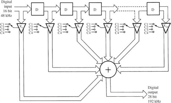
FIGURE 4.13 Twenty-four element digital transversal filter showing a tapped delay line, coefficient multipliers, and an adder.

FIGURE 4.14 A four-times oversampling filter treats input samples as points on a sin(x)/x curve; this reconstructs the output waveform, as in an ideal lowpass filter. In practice, many more samples are needed.
Figure 4.14 illustrates how an oversampling digital filter simulates the effect of an analog filter in waveform reconstruction; specifically, it shows how interpolated samples are computed in a four-times oversampling filter. The input samples I3, I2, I1, and I0 are treated as sin(x)/x impulses placed relative to the center of the filter. Their maximum sin(x)/x impulse response amplitudes are equal to the original sample amplitudes, and the width of the impulse responses are determined by the response of the filter, in this case a filter with a cutoff frequency at the Nyquist frequency of the input samples. The summation of their unique contributions forms the interpolated samples (in practice, as noted, many more than four samples would be present in the filter). Each of the three interpolated samples is formed by adding together the four products, as shown in the figure. Original input samples pass through the filter unchanged by using one set of filter coefficients that contains three zero coefficients and one unity coefficient. In this way, the output sample that coincides with the input sample is unchanged. By multiplying each group of samples (four in this case) with this coefficient set, and three others, interpolated samples are output at a four-times rate.
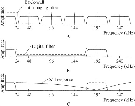
FIGURE 4.15 Image spectra in nonoversampled and oversampled reconstructions. A. A brick-wall filter must sharply bandlimit the output spectra. B. With four-times oversampling, images appear only at the oversampling frequency. C. The output S/H circuit can be used to further suppress the oversampling spectra.
The overall effect of four-times oversampling filtering is shown in Fig. 4.15. A brick-wall filter must sharply bandlimit the output spectra; with oversampling filtering, the images between 24 kHz and 168 kHz (centered at 48, 96, and 144 kHz) are suppressed, leaving the oversampling images. The output S/H circuit can be used to further suppress the oversampling spectra, as shown. In practice, a number of considerations determine the design of oversampling filters. The sin(x)/x waveform extends to infinity in both the positive and negative directions, so theoretically all the values of that infinite waveform would be required to reconstruct the analog signal. Although an analog filter can theoretically access an infinite number of samples for each reconstruction value, a finite impulse response filter, as its name implies, cannot. Thus the oversampling filter is designed to accommodate the number of samples required to maintain an error less than the system’s overall resolution. In the example above, only four coefficients were used, but as many as 300 28-bit coefficients might be needed; in practice, perhaps 100 coefficients would suffice. However, because the sin(x)/x response is symmetrical, only half the coefficients need to be stored in memory; the table can be read bidirectionally. As noted, the multipliers in a digital filter increase the output word length. The output word cannot simply be truncated; this would increase distortion. The word should be redithered.
These examples have used a four-times oversampling filter. However, two-times, four-times, or (most commonly) eight-times digital filters can be used, in which a 48-kHz sampling frequency is oversampled to 96, 192, or 384 kHz, respectively. For example, in an eight-times oversampling filter, seven new audio samples are computed for each input sample, raising the output sampling frequency to 384 kHz. Images are shifted to a band centered at 384 kHz where they are easily removed with a simple analog lowpass filter. Whatever the rate, most oversampling digital filters are similar in operation. However, the characteristic of the analog lowpass filter varies. The lower the oversampling frequency, the closer to the audio band the image spectrum will be, hence the steeper the analog filter response required.
When using traditional D/A converters, a practical limit to the oversampling frequency is reached (around eight times) because most D/A converters cannot operate at faster speeds. On the other hand, D/A converters can more easily convert an oversampling waveform, because the successive changes in amplitude are smaller in an over-sampled signal. More precisely, the slew rate, the rate of variation in the output waveform, is lower. This, along with less ringing and less overshoot, reduces intermodulation distortion. Some designers feel that in oversampling designs of eight times or more, the remaining image spectrum is at such a high frequency that analog filtering can be accomplished with a simple second-order lowpass filter.
In terms of performance, digital filters represent a great improvement over analog filters because a digital filter can be designed with considerable and stable precision. Because digital filtering is a purely numerical process, the characteristics of digital filtering, as opposed to analog filtering, cannot change with temperature, age, and so on. A digital filter might provide an in-band ripple of ±0.00001 dB, with a stopband attenuation of −120 dB. A digital filter can have a linear phase response. High-frequency attenuation due to aperture error can be compensated for in the transversal filter by choosing coefficients to create a slightly rising characteristic prior to cutoff. Digital filter theory is discussed in Chap. 17.
Noise Shaping
Another important benefit of oversampling is a decrease in audio band quantization noise. This is because the total noise power is spread over a larger (oversampled) frequency range. In particular, each doubling of the oversampling ratio R lowers the quantization noise floor by 3 dB (10 log(R) = 10 log(2) = 3.01 dB). For example, in a four-times oversampling filter, data leaves the filter at a four-times frequency, and the quantization noise power is spread over a band that is four times larger, reducing its power density in the audio band to one-fourth, as shown in Fig. 4.16. In this example, this yields a 6-dB reduction in noise (3 dB each time the sampling rate is doubled), which is equivalent to adding one bit of word length. Higher oversampling ratios yield corresponding lower noise (for example, eight-times yields an additional 6 dB).
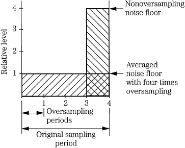
FIGURE 4.16 Oversampling extends quantization error over a larger band, correspondingly reducing in-band error.
Noise shaping, also called spectral shaping, can significantly reduce the in-band noise floor by changing the frequency response of quantization error. The technique is widely used in both A/D and D/A conversion; for example, noise shaping can be accomplished with sigma-delta modulation. When quantization errors are independent, the noise spectrum is white; by selecting the nature of the dependence of the errors, the noise spectrum can be shaped to any desired frequency response, while keeping the frequency response of the audio signal unchanged. Noise shaping is performed by an error-feedback algorithm that produces the desired statistically dependent errors.
In a simple noise shaper, for example, 28-bit data words from the filter are rounded and dithered to create the most significant 16-bit words. The 12 least significant bits (the quantization error that is created) are delayed by one sampling period and subtracted from the next data word, as shown in Fig. 4.17A. The result is a shaped noise floor. The delayed quantization error, added to the next sample, reduces quantization error in the output signal; the quantization noise floor is decreased by about 7 dB in the audio band, as shown in Fig. 4.17B. As the input audio signal changes more rapidly, the effect of the error feedback decreases; thus quantization error increases with increasing audio frequency. For example, approaching 96 kHz, the error feedback comes back in phase with the input, and noise is maximized, as also shown in Fig. 4.17B. However, the out-of-band noise is high in frequency and thus less audible, and can be attenuated by the output filter. This trade-off of low in-band noise, at the expense of higher out-of-band noise, is inherent in noise shaping. Noise shaping is used, and must be used, in low-bit converters to yield a satisfactorily low in-band noise floor. Noise shaping is often used in conjunction with oversampling. When the audio signal is oversampled, the bandwidth is extended, creating more spectral space for the elevated high-frequency noise curve.
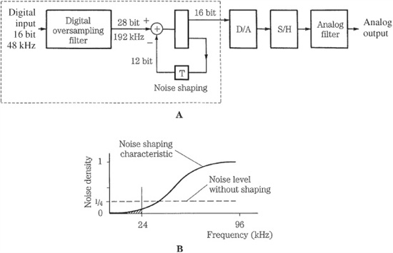
FIGURE 4.17 Noise shaping following oversampling decreases in-band quantization error. A. Simple noise-shaping loop. B. Noise shaping suppresses noise in the audio band; boosted noise outside the audio band is filtered out.
In practice, oversampling sigma-delta A/D and D/A converters are widely used. For example, an oversampling A/D converter may capture an analog signal using an initial high sampling frequency and one-bit signal, downconvert it to 48 kHz and 16 bits for storage or processing, then the signal may be upconverted to a 64- or 128-times sampling frequency for D/A conversion. Sigma-delta modulation and noise shaping is discussed in Chap. 18.
Noise shaping can also be used without oversampling; the quantization error remains in the audio band and its average power spectral density is unchanged, but its spectrum is psychoacoustically shaped according to the ear’s minimum audible threshold. In other words, the level of the noise floor is higher at some in-band frequencies, but lower at others; this can render it significantly less audible. Psychoacoustically optimized noise shaping is discussed in Chap. 18.
Output Processing
Following digital filtering, the data is converted back to analog form with a D/A converter. In the case of four-times oversampling, with a sampling frequency of 48 kHz, the aperture effect of an output S/H circuit creates a null at 192 kHz, further suppressing that oversampling image. As noted, designing a slight high-frequency boost in the digital filter can compensate for the slight attenuation of high audio frequencies. The remaining band around 192 kHz can be completely suppressed by an analog filter. This low-order anti-imaging filter follows the D/A converter. Because the oversampling image is high in frequency, a filter with a gentle, 12-dB/octave response and a −3 dB point between 30 and 40 kHz is suitable; for example, a Bessel filter can be used. It is a noncritical design, and its low order guarantees good phase linearity; phase distortion can be reduced to ±0.1° across the audio band. Oversampling can decrease in-band noise by 6 dB, and noise shaping can further decrease in-band noise by 7 dB or more. Thus, with an oversampling filter and noise shaping, even a D/A converter with 16-bit resolution can deliver good performance.
Alternate Coding Architectures
Linear PCM is considered to be the classic audio digitization architecture and is capable of providing high-quality performance. Other digitization methods offer both advantages and disadvantages compared to PCM. A linear PCM system presents a fixed scale of equal quantization intervals that map the analog waveform, while specialized systems offer modified or wholly new mapping techniques. One advantage of specialized techniques is often data reduction, in which fewer bits are needed to encode the audio signal. Specialized systems are thus more efficient, but a penalty might be incurred in reduced audio fidelity.
In a fixed linear PCM system, the quantization intervals are fixed over the signal’s amplitude range, and they are linearly spaced. The quantizer word length determines the number of quantization intervals available to encode a sample’s amplitude. The intervals are all of equal amplitude and are assigned codes in monotonic order. However, both of these parameters can be varied to yield new digitization architectures.
Longer word lengths reduce quantization error; however, this requires a corresponding increase in data bandwidth. Uniform PCM quantization is optimal for a uniformly distributed signal, but the amplitude distribution of most audio signals is not uniform. In some alternative PCM systems, quantization error is minimized by using nonuniform quantization step sizes. Such systems attempt to tailor step sizes to suit the statistical properties of the signal. For example, speech signals are best served by an exponential-type quantization distribution; this assumes that small amplitude signals are more prevalent than large signals. Many quantization levels at low amplitudes, and fewer at high amplitudes, should result in decreased error. Companding, with dynamic compression prior to uniform quantization, and expansion following quantization, can be used to achieve this result. Floating point systems use range-changing to vary the signal’s amplitude to the converter, and thus expand the system’s dynamic range. A greatly modified form of PCM is a differential system called delta modulation (DM). It uses only one bit for quantizing; however, a very high sampling frequency is required. Other forms of delta modulation include adaptive, companded, and predictive delta modulation. Each offers unique strengths and weaknesses. Low bit-rate, based on psychoacoustics, is discussed in Chaps. 10 and 11.
Floating-Point Systems
Floating-point systems use a PCM architecture modified to accept a scaling value. It is an adaptive approach, with nonuniform quantization. In true floating-point systems, the scaling factor is instantaneously applied from sample to sample. In other cases, as in block floating-point systems, the scale factor is applied to a relatively large block of data.
Instead of forming a linear data word, a floating-point system uses a nonuniform quantizer to create a word divided into two parts: the mantissa (data value) and exponent (scale factor). The mantissa represents the waveform’s uniform value and its scaled amplitude; the quantization step size is represented by the exponent. In particular, the exponent acts as a scalar that varies the gain of the signal in the PCM A/D converter. By adjusting the gain of the signal, the A/D converter is used more efficiently. Low-level signals are boosted and high-level signals are attenuated; specifically, a signal’s level is set to the highest possible level that does not exceed the converter’s range. This effectively varies the quantization step size according to the signal amplitude and improves accuracy of low-level signal coding, the condition where quantization error is relatively more problematic. Following D/A conversion, the gain is again adjusted to correspond to its original value.
For example, consider a floating-point system with a 10-bit mantissa (A/D converter), and 3-bit exponent (gain select), as shown in Fig. 4.18. The 3-bit exponent provides eight different ranges for a 10-bit mantissa. This is the equivalent multiplicative range of 1 to 128. The maximum signals are −65,536 to 65,408. In this way, 13 bits cover the equivalent of a 17-bit dynamic range, but only a 10-bit A/D converter is required. However, large range and small resolution are not simultaneously available in a floating-point system because of its nonuniform quantization. For example, although 65,408 can be represented, the next smallest number is 65,280. In a linear PCM system, the next smallest number is, of course, 65,407. In general, as the signal level increases, the number of possible quantization intervals decreases; thus, quantization error increases and the S/N ratio decreases. In particular, the S/N ratio is signal-dependent, and less than the dynamic range. In various forms, an exponent/mantissa representation is used in many types of systems.
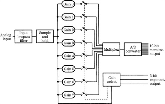
FIGURE 4.18 A floating-point converter uses multiple gain stages to manipulate the signal’s amplitude to optimize fixed A/D conversion.
A floating-point system uses a short-word A/D converter to achieve a moderate dynamic range, or a longer-word converter for a larger dynamic range. For example, a floating-point system using a 16-bit A/D converter and a 3-bit exponent adjusted over a 42-dB range in 6-dB steps would yield a 138-dB dynamic range (96 dB + 42 dB). This type of system would be useful for encoding particularly extreme signal conditions. In addition, this floating-point system only requires a split 19-bit word, but the equivalent fixed linear PCM system would require a linear 23-bit word. In addition, when the gain stages are placed at 6-dB intervals, the coded words can be easily converted to a uniform code for processing or storage without computation. The mantissa undergoes a shifting operation according to the value of the exponent.
Although a floating-point system’s dynamic range is large, the nature of its dynamic range differs from that of a fixed linear system; it is inherently less than its S/N ratio. This is because dynamic range measures the ratio between the maximum signal and the noise when no signal is present. With the S/N ratio, on the other hand, noise is measured when there is a signal present. In a fixed linear system, the dynamic range is approximately equal to the S/N ratio when a signal is present. However, in a floating-point system, the S/N ratio is approximately determined by the resolution of the fixed A/D converter (approximately 6n), which is independent of the larger dynamic range. Changes in the signal dictate changes in the gain structure, which affect the relative amplitude of quantization error.
The S/N ratio thus continually changes with exponent switching. For example, consider a system with a 10-bit mantissa and 3-bit exponent with 6-dB gain intervals. The maximum S/N ratio is 60 dB. As the input signal level falls, so does the S/N ratio, falling to a minimum of 54 dB until the exponent is switched, and the S/N again rises to 60 dB. For longer-word converters, a complex signal will mask the quantization error. However, in the case of simple tones, the error might be audible. For example, modulation noise from low-frequency signals and quantization noise from nearly inaudible signals might result. Another problem can occur with gain switching; inaccuracies in calibration might present discontinuities as the different amplifiers are switched.
The changes in the gain structure can affect the audibility of the error. Instantaneous switching from sample to sample tends to accentuate the problem. Instead, gain switching should be performed with algorithms that follow trends in signal amplitude, based on the type of program to be encoded. For example, syllabic algorithms are adapted to the rate at which syllables vary in speech. Gain decreases are instantaneous, but gain increases are delayed. This approximates a block floating-point system, as described below. In any event, the gain must be switched to prevent any overload of the A/D converter.
Block Floating-Point Systems
The block floating-point architecture is derived from the floating-point architecture. Its principal advantage is data reduction making it useful for bandlimited transmission or storage. In addition, a block floating-point architecture facilitates syllabic or other companding algorithms.
In a block floating-point system, a fixed linear PCM A/D converter precedes the scalar. A short duration of the analog waveform (1 ms, for example) is converted to digital data. A scale factor is calculated to represent the largest value in the block, and then the data is scaled upward so the largest value is just below full scale. This reduces the number of bits needed to represent the signal. The data block is transmitted, along with the single scale factor exponent.
During decoding, the block is properly rescaled. In the example in Fig. 4.19, 16-bit words are scaled to produce blocks of 10-bit words, each with one 3-bit exponent. Because only one exponent is required for the entire data block, data rate efficiency is increased over conventional floating-point systems. The technique of sending one scale factor per block of audio data is used in many types of systems.
Block floating-point systems avoid many of the audible artifacts introduced by instantaneous scaling. The noise amplitude lags the signal amplitude by the duration of the buffer memory (for example, 1 ms); because this delay is short compared to human perception time, it is not perceived. Thus, a block floating-point system can minimize any perceptual gain error.
Floating-point systems work best when the audio signal has a low peak-to-average ratio for short durations. Because most acoustical music behaves in this manner, system performance is relatively good. An instantaneous floating-point system excels when the program varies rapidly from sample to sample (as with narrow, high-amplitude peaks) yet is inferior to a fixed linear system. Performance dependence on program behavior is a drawback of many alternative (non-PCM) digitization systems.
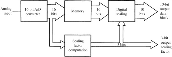
FIGURE 4.19 A block floating-point system uses a scaling factor over individual blocks of data.
Nonuniform Companding Systems
With linear PCM, quantization intervals are spaced evenly throughout the amplitude range. As we have observed, the range changing in floating-point systems provides a nonuniform quantization. Nonuniform companding systems also provide quantization steps of different sizes, but with a different approach, called companding. Although companding is not an optimal way to achieve nonuniform quantization, its ease of implementation is a benefit.
In nonuniform companding systems, quantization levels are spaced far apart for high-amplitude signals, and closer together for low-amplitude signals. This follows the observation that in some types of signals, such as speech, small amplitudes occur more often than high amplitudes. In this way, quantization is relatively improved for specific signal conditions. This nonuniform distribution is accomplished by compressing and expanding the signal, hence the term, companding. When the signal is compressed prior to quantization, small values are enhanced and large values are diminished. As a result, perceived quantization noise is decreased.
A logarithmic function is used to accomplish companding. Within the compander, a linear PCM quantizer is used. Because the compressed signal sees quantization intervals that are uniform, the conversion is equivalent to one of nonuniform step sizes. On the output, an expander is used to inversely compensate for the nonlinearity in the reconstructed signal. In this way, quantization levels are more effectively distributed over the audio dynamic range.
A companding system is shown in Fig. 4.20. The encoded signal must be decoded before any subsequent processing. Higher amplitude signals are more easily encoded, and lower amplitude signals have reduced quantization noise. This results in a higher S/N ratio for small signals, and it can increase the overall dynamic range compared to fixed linear PCM systems. Noise increases with large amplitude audio signals and is correlated; however, the signal amplitude tends to mask this noise. Noise modulation audibility can be problematic for low-frequency signals with quickly changing amplitudes.
l-Law and A-Law Companding
The μ-law and A-law systems are examples of quasi-logarithmic companding, and are used extensively in telecommunications to improve the quality of 8-bit quantization. Generally, the quantization distribution is linear for low amplitudes, and logarithmic for higher amplitudes. The μ-law and A-law standards are specified in the International Telecommunications Union (ITU) recommendation G.711.
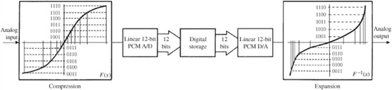
FIGURE 4.20 A nonlinear conversion system uses companding elements before and after signal conversion.
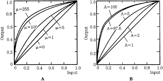
FIGURE 4.21 Companding characteristics determine how the quantization step size varies with signal level. A. μ-law characteristic. B. A-law characteristic.
The μ-law encoding method was developed to code speech for telecommunications applications. It was developed for use in North America and Japan. The audio signal is compressed prior to quantization and the inverse function is used for expansion. The value of 0 corresponds to linear amplification, that is, no compression or uniform quantization. Larger values result is greater companding. A μ = 255 system is often used in commercial telecommunications. An 8-bit implementation can achieve a small-signal S/N ratio and dynamic range that are equivalent to that of a 12-bit uniform PCM system. The A-law is a quantization characteristic that also varies quasi-logarithmically. It was developed for use in Europe and elsewhere. An A = 87.56 system is often employed using a midrise quantizer. Figure 4.21 shows μ-law and A-law companding functions for several values of μ and A. The μ-law and A-law transfer functions are very similar, but differ slightly for low-level input signals.
Generally, logarithmic PCM methods such as these require about four fewer bits per sample for speech quality equivalent to linear PCM; for example, 8 bits might be sufficient, instead of 12. Because speech signals are typically sampled at 8 kHz, the standard data rate for μ-law or A-law PCM data is therefore 64,000 bits/second (or 64 kbps). The device used to convert analog signals to/from compressed signals is often called a codec (coder/decoder).
Differential PCM Systems
Differential PCM (DPCM) systems are unlike linear PCM methods. They are more efficient because they code differences between samples in the audio waveform. Intuitively, it is not necessary to store the absolute measure of a waveform, only how it changes from one sample to the next. The differences between samples are often smaller than the amplitudes of the samples themselves, so fewer bits should be required to encode the possible range of signals. Furthermore, a waveform’s average value should change only slightly from one sample to the next if the sampling frequency is fast enough; most sampled signals show significant correlation between successive samples. Differential systems thus exploit the redundancy from sample to sample, using a few PCM bits to code the difference in amplitude between successive samples. The quantization error can be smaller than with traditional waveform PCM coding. Depending on the design, differential systems can use uniform or nonuniform quantization.
The rate at which signal voltage can change is inherently limited in DPCM systems; the coded signal amplitude decreases at 6 dB/octave; thus the S/N ratio decreases at 6 dB/octave. The frequency response of the coded signal can be filtered to improve the S/N ratio. For example, a signal with little high-frequency content can be filtered to increase high frequencies; this is reversed during decoding, and noise is relatively masked by the low-frequency content.
Predictive Differential Coding
Differential systems use a form of predictive coding. The technique predicts the value of the current sample based on values of previous samples, and then codes the difference between the predicted value and the unquantized input sample value. In particular, a predicted signal is subtracted from the actual input and the difference signal (the error) is quantized. The decoder produces the prediction from previous samples; using the prediction and the difference value, the waveform is reconstructed sample by sample. When the prediction is accurate and the error signal is small, predictive coding requires fewer bits to quantize an audio signal, but performance depends on the type of function used to derive the prediction signal and its ability to anticipate the changing signal. Compared to PCM systems, differential systems are cost-effective in hardware, provide data rate efficiency, and are perceptually less affected by bit errors.
Delta Modulation
As noted, differential systems encode the difference between the input signal and a prediction. As the sampling frequency increases, the possible amount of change between samples decreases and encoding resolution increases. Delta modulation (DM) is the simplest form of differential PCM. It uses a very high sampling frequency so that only a one-bit quantization of the difference signal is used to encode the audio waveform. Conceptual operation of a delta modulation system is shown in Fig. 4.22. Positive or negative transitions in the quantized waveform are used to encode the audio signal. Because the staircase can move from sample to sample by only one fixed quantization interval, a fast sampling frequency is required to track the signal’s transients. In the example in Fig. 4.22, the sampling frequency is insufficient to track the signal’s rise time. In this slope-overload condition, the differential itself is encoded, rather than the original signal.
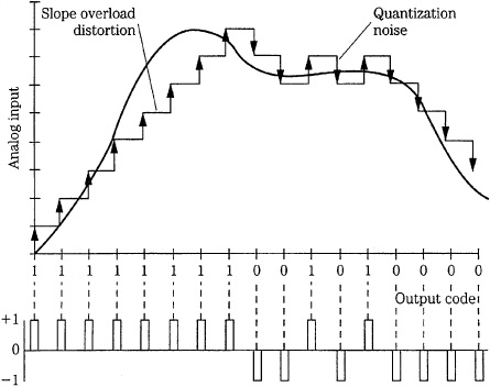
FIGURE 4.22 In a delta-modulation coder, one differential bit is used to encode the audio signal.
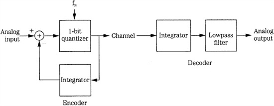
FIGURE 4.23 Delta-modulation encoder and decoder.
Delta modulation is efficient from a hardware standpoint, as shown in Fig. 4.23. Integrators are used as first-order predictors. The difference between the input signal and its predicted value is quantized as a one-bit correcting word and generated at sample time. The system determines if the sign of its error is positive or negative, and applies the sign (a positive or negative pulse) to the integrator that correspondingly moves its next value up or down one increment, always closer to the present value. The accuracy of the encoding rests on the size of the increment, or step. Also, the signal must change at each sample; it cannot be constant. At the output, the correction signal is decoded with an integrator to estimate the input signal. As with any DPCM system, the coded signal amplitude decreases with frequency, so the S/N ratio decreases by 6 dB/octave. Only one correction can occur per sample interval, but a very fast rate could theoretically allow tracking of even a fast-transient audio waveform. Delta modulation offers excellent error performance. In a linear PCM system, an uncorrected MSB error results in a large discontinuity in the signal. With delta modulation, there is no MSB. Each bit merely tracks the difference between samples, thus inherently limiting the amount of error to that difference. The possibility of degradation, however, necessitates error correction. Parity bits and interleaving are commonly used for this purpose.
From a practical standpoint, DM fails to perform well in high-fidelity applications because of its inherent trade-off between sampling frequency and step size. Encoding resolution is directly dependent on step size. The smaller the steps, the better the approximation to the audio signal, and the lower the quantization error. However, when the encoding bit cannot track a complex audio waveform that has low sample-to-sample correlation, slew rate limitations yield transient distortion. The sampling frequency can be increased with oversampling to compensate, but the rates required for successful encoding of wide bandwidth signals are extreme. Perceptually, when slope overload is caused by high-frequency energy, the signal tends to mask the distortion. Quantization error is always present, and is most audible for low-amplitude signals. To make the best of the circumstances, step size can be selected to minimize the sum of the mean squares of the two distortion values from slope overload and quantization. Timothy Darling and Malcolm Hawksford have shown that the signal to quantization error ratio of a delta modulation system can be expressed as:
where fs = sampling frequency
fb = noise bandwidth
fi = audio (sine-wave) frequency
To achieve a 16-bit PCM S/N ratio of 96 dB over a 20 kHz bandwidth, a DM system would require clocking at 200 MHz. Although a doubling of bit rate in DM results in an increase in S/N of 9 dB, a doubling of word length in PCM produces an exponential S/N increase. From an informational standpoint, we can see that the nature of DM hampers its ability to encode audio information. A sampling frequency of 500 kHz, for example, would theoretically permit encoding of frequencies up to 250 kHz, but that bandwidth is largely wasted because of the relatively low frequency of audio signals. In other words, the informational encoding distribution of delta modulation is inefficient for audio applications.
On the other hand, the high sampling frequency required for delta modulation offers one benefit. As observed with noise shaping, for each doubling of sampling frequency, the noise in a fixed band decreases by 3 dB. The total noise remains constant, but it is spread over a larger spectrum thus in-band noise is reduced. This somewhat lowers the noise floor in a DM system. In addition, because of the high sampling frequency, brick-wall filters are not required. Low-order filters can provide adequate attenuation well before the half-sampling frequency without affecting audio response. Of course, conventional A/D and D/A converters are not required. Ultimately, because of its limitations, delta modulation is not often used for high-fidelity applications. However, a variation known as sigma-delta modulation offers excellent results and is widely used in oversampling A/D and D/A converters, as discussed in Chap. 18. The Super Audio CD (SACD) format uses Direct Stream Digital (DSD) coding, a one-bit pulse density method using sigma-delta modulation. SACD is discussed in Chap. 7.
Adaptive Delta Modulation
Adaptive delta modulation (ADM) systems vary quantization step sizes to overcome the transient response limitations of delta modulation. At the same time, quantization error is held to a reasonable value. A block diagram of an ADM encoder is shown in Fig. 4.24A. The encoder examines input data to determine how to best adjust step size. For example, with a simple adaptive algorithm, a series of all-positive or all-negative difference bits would indicate a rapid change from the approximation. The step size would increase to follow the change either positively or negatively. The greater the overload condition, the larger the step size selected. Alternating positive and negative difference bits indicate good tracking, and step size is reduced for even greater accuracy, as shown in Fig. 4.24B. This yields an increase in S/N, with no increase in sampling frequency or bit rate. As more bits in the stream are devoted to diagnosing signal behavior, step size selection can be improved.
ADM design is complicated because the decoder must be synchronized to the step size strategy to recognize the variation. Also, it can be difficult to change step size quickly and radically enough to accommodate sharp audio transients. As high-frequency and high-amplitude signals demand large increments, quantization noise is increased, producing noise modulation with a varying noise floor. In addition, it is difficult to inject a dither signal in an ADM system; since the step size changes, a fixed amount of dither is ineffective. Error feedback can reduce in-band noise. A pre-emphasis filter characteristic can reduce subjective noise in small-amplitude signals, mask the change in noise with changing step size, and reduce low-frequency noise in high-amplitude, high-frequency signals. As the audio slope increases, a control signal from the delta modulator, the same signal used to control step size, raises the frequency of the highpass filter and attenuates low frequencies. Another variation of ADM is continuously variable slope delta modulation (CVSDM), in which step size is continuously variable, rather than incremental.
FIGURE 4.24 Operation of an adaptive delta modulation encoder. A. Block diagram of an adaptive delta modulation encoder with variable step size. B. Changes in step size are triggered by continuous 1s or 0s.
Companded Predictive Delta Modulation
Companded predictive delta modulation (CPDM) rejects ADM in favor of a compander delta modulation scheme. Instead of varying the step size in relation to the signal, the signal’s amplitude is varied prior to the constant step size delta modulator to protect against modulator overload. To reduce the quantization noise floor level, a linear predictive filter is used, in which an algorithm uses many past samples to better predict the next sample.
The companding subsystem consists of a digitally controlled amplifier in both the encoder and decoder, for controlling broadband signal gain. The bitstream itself controls both amplifiers to minimize tracking error. The digitally controlled amplifiers continually adjust the signal over a large range to best fit the fixed step size of the delta modulator. A transient “speed-up” circuit in the level sensing path allows faster gain reduction during audio transients. Strings of 1s or 0s indicate the onset of an overload, and trigger compression of broadband gain to ensure that the transients are not clipped at the modulator. The speed of the gain change can be either fast or slow, depending on the audio signal dynamics. Spectral compression can be used to reduce variations in spectral content; the circuit could reduce high frequencies when the input spectrum contains predominantly high frequencies, and boost high frequencies when the spectrum is weighted with low frequencies. The spectrum at the A/D converter is thus more nearly constant.
Adaptive Differential Pulse-Code Modulation
Adaptive differential pulse-code modulation (ADPCM) combines the predictive and adaptive difference signal of ADM with the binary code of PCM to achieve data reduction. Although designs vary, in many cases the difference signal to be coded is first scaled by an adaptive scale factor, and then quantized according to a fixed quantization curve. The scale factor is selected according to the signal’s properties; for example, the quantizer step size can be varied in proportion to the signal’s average amplitude. Signals with large variations cause rapid changes in the scale factor, whereas more stable signals cause slow adaptation. Step size can be effectively varied by either directly varying the step size, or by scaling the signal with a gain factor.
A linear predictor, optimized according to the type of signal to be coded, is used to output a signal estimate of each sample. This signal is subtracted from the actual input signal to yield a difference signal; this difference signal is quantized with a short PCM word (perhaps 4 or 8 bits) and output from the encoder. In this way, the signal can be adaptively equalized, and the quantization noise adaptively shaped, to help mask the noise floor for a particular application. For example, the noise can be shaped so that its spectrum is white after decoding. Noise shaping is described in Chap. 18.
The decoder performs the same operations as the encoder; by reading the incoming data stream, the correct step size is selected, and the difference signal is used to generate the output samples. Lowpass filtering is applied to the output signal. The benefit of ADPCM is bit-rate reduction based on the tendency for amplitude and spectrum distribution of audio signals to be concentrated in a specific region. The scale factors and other design elements in an ADPCM algorithm take advantage of these statistical properties of the audio signal. In speech transmission applications, a bit rate of 32 kbps (kilobits per second) is easily achieved.
ADPCM’s performance is competitive, or relatively superior to that of fixed linear PCM. When the audio signal remains near its maximum frequency, ADPCM’s performance is similar to PCM’s. However, this is rarely the case with audio signals. Instead, the instantaneous audio frequency is relatively low, thus the signal changes more slowly, and amplitude changes are smaller. As a result, ADPCM’s quantization error is less than that of PCM. In theory, given the same number of quantization bits, ADPCM can achieve better signal resolution. In other words, relatively fewer bits are needed to achieve good performance. In practice, a 4-bit ADPCM signal might provide fidelity subjectively similar to an 8-bit PCM signal.
Variations of the ADPCM algorithm are used in many telecommunications standards. The ITU-T Recommendation G.721 uses ADPCM operating at 32 kbps. G.722 contains another example of an ADPCM coder. G.723 uses ADPCM at bit rates of 24 to 40 kbps. G.726 specifies a method to convert 64 kbps μ-law or A-law PCM data to 16-, 24-, 32-, or 40-kbps ADPCM data. The bit rate of 32 kbps is used for speech applications. In the G.726 standard, both the quantizer and predictor adapt to input signal conditions. The G.727 standard uses ADPCM at bit rates of 16, 24, 32 and 40 kbps. The G.727 standard can also be used within the G.764 standard for packet network applications. Speech coding is described in more detail in Chap. 12.
The CD-ROM/XA format uses several ADPCM coding levels to deliver fidelity according to need. An 8-bit ADPCM quality level can yield an S/N ratio of 90 dB, and bandwidth of 17 kHz. The two 4-bit levels yield an S/N of 60 dB, and bandwidths of 17 kHz and 8.5 kHz. During encoding, the original audio data frequency (44.1 kHz) is reduced by a sampling rate converter to a lower frequency (37.8 kHz or 18.9 kHz) depending on the quality level selected. The original word length (16 bits) is reduced (4 or 8 bits) per sample with ADPCM encoding. Four different prediction filters can be selected to optimize the instantaneous S/N ratio; a filter is selected for a block of 28 samples depending on the spectral content of the signal. Companding and noise shaping are also used to increase dynamic range. The filter type is described in each data block. During ADPCM decoding, the audio data is block-decoded and expanded to a linear 16-bit form. Depending on audio quality level, this ADPCM encoder can output from 80 to 309 kbps/channel, yielding a reduced data rate. ADPCM with a 4:1 compression ratio is sometimes used in QuickTime software, and Windows software may use ADPCM coding in .aiff and .wav files. ADPCM also appears in video-game platforms.
Unlike perceptual coding algorithms, ADPCM encoding and decoding may be executed with little processor power. For example, the Interactive Multimedia Association (IMA) version of ADPCM is quite concise. Four bits can be used to store each sample. The encoder finds the difference between two samples, divides it by the current step size and outputs that value. To create the next sample, the decoder multiplies this value by the current step size and adds it to the result of the previous sample. The step size is not stored directly. Instead, a table of possible step sizes (perhaps 88 entries) is used; the entries follow a quasi-exponential progression. The decoder references the table, using previous values to correctly update the step size. When the scaled difference is small, a smaller step size is selected; when the difference is large, a larger step size is selected. In this way, ADPCM coding may be efficiently performed in software.
ADPCM, as well as other specialized designs, offer alternatives to classic linear PCM design. They adhere to the same principles of sampling and quantizing; however, their implementations are quite different. Perceptual coding systems are commonly used to code audio signals when bit rate is the primary concern; these systems are discussed in Chaps. 10 and 11.
Timebase Correction
As we observed in Chap. 3, modulation coding is used in storage and transmission channels to improve coding efficiency and, for example, make the data self-clocking. However, successful recovery of data is limited by the timebase accuracy of the received clock. For example, speed variations in the transport of an optical disc player, instability imposed on a data stream’s embedded clock, and timing inaccuracies in the oscillator used to clock an A/D or D/A converter can all lead to degraded performance in the form of data errors, or noise and modulation artifacts in the converted waveform. For successful recovery of data, receiver circuits must minimize timebase errors that occur in the storage medium, during transmission, or within regeneration and conversion circuitry itself. For example, phase-locked loops (PLLs) are often used to resynchronize a receiver with the transmitted channel code’s clock.
Timing accuracy is challenging in the digital environment, because of the noise and interference that is present. Moreover, tolerances needed for timebase control increase with word length; for example, 20-bit conversion requires much greater timebase accuracy than 16-bit conversion. Above all, timing stability can be problematic because of the absolute tolerances it demands. A clock might require timing accuracy of 20 ps (picoseconds). Note that a picosecond is the reciprocal of 1 THz (terahertz), which is 1000 GHz (gigahertz), which is 1,000,000 MHz.
Jitter
Any deviation in the zero-crossing times of a data waveform from the zero-crossing times of a perfectly stable waveform can be characterized as jitter. In particular, it is the time-axis instability of a waveform measured against an ideal reference with no jitter. Timing variations in an analog signal may be directly audible as pitch instability. However, jitter in a digital signal may cause bit errors in the bitstream or be indirectly audible as increased noise and distortion in the output analog waveform or, if the digital signal is correctly de-jittered, there may be no bit errors or audible effects at all. Jitter is always present; its effect and the required tolerance depend on where in the signal processing chain the jitter occurs. Relatively high jitter levels will not prevent error-free transfer of data from one device interfaced to another, but some interface devices are less tolerant of jitter than others. During A/D or D/A conversion, even low jitter levels can induce artifacts in the analog output waveform; some converters are also less tolerant of jitter than others.
Jitter manifests itself as variations in the transition times of the signal, as shown in Fig. 4.25. Around each ideal transition is a period of variation or uncertainty in arrival time; this range is called the peak-to-peak jitter. Jitter occurs in data in a storage medium, transmission channel, or processing or regeneration circuits such as A/D and D/A converters. Jitter can occur as random variations in clock edges (white phase jitter), it can be related to the width of a clock pulse (white FM jitter), or it can be related to other events (correlated jitter), sometimes periodically.
FIGURE 4.25 A time variation in the medium, or regeneration or processing circuits, results in a timebase jitter error.
Jitter is best described by its spectral characteristics; this shows the amplitude and frequency of the jitter signal. Random jitter will show a broadband spectrum; when the data is reconstructed as an analog waveform it will have an increased noise floor. Periodic jitter will appear as a single spectral line; FM sidebands or modulated noise could appear in the reconstructed signal, spaced on either side of the signal frequency. Jitter at frequencies less than the sampling frequency causes a timing error to accumulate; the error depends on the amplitude and frequency of the modulation waveform. Generally, peak-to-peak jitter is a valid measure; however, when the jitter is random, a root mean square (rms) jitter measure is valid. Care must be taken when specifying jitter; for example, if the deviation in a clock signal’s period width is averaged over time, the average can converge to zero, resulting in no measured jitter.
Eye Pattern
An oscilloscope triggered from a stable reference clock, and timebase set at one unit interval (UI), will display a superimposed successive transition known as the eye pattern. (A reference clock can be approximated by a phase-locked low-jitter clock.) The eye pattern can be used to interpret the quality of the received signal. It will reveal noise as the waveform’s amplitude variations become indistinct, and jitter as the transitions shift about time intervals of the code period. Peak shift, dc offset, and other faults can be observed as well. The success in regeneration can similarly be evaluated by examining the eye pattern after processing. Noise in the channel will tend to close the pattern vertically (noise margin), and jitter closes it horizontally (sampling time margin), as shown in Fig. 4.26, possibly degrading performance to the point where pulse shaping can no longer accurately retrieve the signal. The amount of deterioration can be gauged by measuring the extent of amplitude variations, and forming an eye opening ratio:
where a1 = outside amplitude
a2 = inside amplitude
Δa = amplitude variation
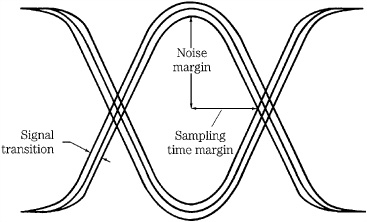
FIGURE 4.26 The eye pattern can be used to interpret the quality of an RF data signal. A minimum inside eye opening size determines the limit of a signal’s usability. If the eye closes, errors will result.
Both variations are measured from the center of the opening in the eye pattern. The eye height is specified in volts, and eye width in bit time or percent of cell period. The width of the eye gives the percentage of the data period available to ascertain its logical value, and the height shows the maximum difference between these levels during the available time. The receiver is generally able to read the signal if the eye opening has at least a minimum interior size and is maintained at coded intervals; the center of the eye shows the amplitude level decision threshold and the sampling time. However, jitter introduced into the receiver’s clock recovery circuits will cause the receiver to sample the data further from the center of the data cell.
Jitter observed on an oscilloscope shows the dynamic variations in the signal, but a more careful method applies the data signal to an FM demodulator, which is connected to a spectrum analyzer. Random jitter exhibits a broadband spectrum and raises the noise floor in the analog signal reconstructed from the data. Periodic jitter will appear as a single spectral line, at a low frequency for a slow clock variation or at a high frequency for a fast clock variation; the reconstructed signal may contain FM sidebands or modulated noise.
Interface Jitter and Sampling Jitter
The significance of jitter depends on where in the signal chain it is considered. For example, it is important to distinguish between interface jitter (which occurs in digital-to-digital data transfer) and sampling jitter (which occurs when converting data into and out of the digital domain). Interface timing errors are distinct from those caused by sampling jitter. Interface jitter occurs in transmitted data clocks, when conveying data from one device to another.
Interface jitter is a concern if it causes uncorrected errors in the recovered signal; the quality of transmitted data can be monitored by error detection circuits at the receiver. Many data streams are self-clocking; a receiver must recover the clock and hence the data by synchronizing to the transmitted clock. A receiving circuit with a fixed clock would not be able to lock onto a signal with unregulated timing variations in the received clock, even if its rate was nominally equal to the received clock rate. For this reason, receiving circuits commonly use a phase-locked loop (PLL) circuit to align their clocks with the data rate of the incoming signal. An interface PLL, as shown in Fig. 4.27, acts like a mechanical flywheel, using its lowpass filter characteristic to attenuate short-term fluctuations in the signal timing. It tracks the slowly changing data signal, but strips off its quickly changing jitter. A PLL accepts the input signal as a timing reference, measures the phase error between the input signal and its own output through a feedback loop and uses the error to control a voltage-controlled oscillator (VCO) within the loop. In response, the VCO reaches equilibrium by minimizing this loop phase error. Once the VCO is locked to the phase of the input signal, the oscillator runs at the reference frequency or a multiple of it. The oscillator is decoupled from the reference, attenuating high-frequency jitter on the PLL’s output data. A PLL can thus provide jitter reduction by reclocking signals to an accurate and stable timebase. Adversely, at lower jitter frequencies relative to the filter’s corner frequency, a PLL’s jitter attenuation will be reduced. At low jitter frequencies, the PLL will track the jitter and pass it on (a second PLL stage with a lower corner frequency might be needed). Moreover, any gain near the cutoff frequency of the PLL’s lowpass filter function would increase jitter.
FIGURE 4.27 An example of an interface phase-locked loop. The PLL’s limited bandwidth prevents jitter from passing through the PLL on the output data or output clock.
If the recovered data is free of errors, interface jitter has not affected it. However, if subsequent reclocking circuits do not remove jitter from the recovered data, potentially audible artifacts can result from sampling jitter at the D/A converter. Sampling jitter can affect quality of an audio signal as it is sampled or resampled with this timing error. Sampling jitter can be induced by sampling clocks, and affects the quality of the reproduced signal, adding noise and distortion. Timing tolerances must be very tight so that timing errors in a recovered clock are minimized. The clock generating circuits used in a sampling device may derive a timing reference from the interface signal. In this case, a PLL might be needed to remove interface jitter to yield a sample clock that is pure enough to avoid potentially audible jitter modulation products.
Jitter can occur throughout the signal chain so that precautions must be taken at each stage to decouple the bitstream from the jitter, so data can be passed along without error. This is particularly important in a chain of connected devices because jitter will accumulate in the throughput signal. Each device might contribute a small amount of jitter, as will the interface connections, eventually leading to data errors or conversion artifacts. Even a badly jittered signal can be cleaned by retiming it through jitter attenuation. With proper means, the output data is correct in frequency and phase, with propagated jitter within tolerance.
Jitter in Mechanical Storage Media
Jitter must be controlled throughout the audio digitization chain, beginning at the mechanical storage media. Storage media such as optical disc can impose timebase errors on the output data signal because of speed variations in the mechanical drives they use. Accurate clocks and servo systems must be designed to limit mechanical speed variations, and input and output data must be buffered to absorb the effects of data irregularities. Speed variations in the transport caused by eccentricities in the rotation of spindle motors will cause the data rate to vary; the transport’s speed can slowly drift about the proper speed, or fluctuate rapidly. If the amount of variation is within tolerance, that is, if the proper value of the recorded data can be recovered, then no error in the signal results.
Servo control circuits are used to read timing information from the output data and generate a transport correction signal. In many cases, a PLL circuit is used to control the servo, as shown in Fig. 4.28. Speed control can be achieved with a PLL by comparing the synchronization words in the output bitstream (coded at a known rate) to a reference, and directing a speed control servo voltage to the spindle motor to dynamically minimize the difference. Fine speed control can use a second PLL, for example, to achieve constant linear velocity in an optical disc drive.
FIGURE 4.28 An example of a servo-pulse extractor/control loop used to control disc speed.
Although phase-locked servo systems act to maintain accurate and constant speed of the mechanical storage medium, timebase errors can still exist in the data. Likewise, jitter might be encountered whenever data is transmitted through an electrical or optical interconnection. To minimize the effect of timebase variations, data is often reclocked through a buffer. A buffer memory effectively increases the capture range for a data signal; for example, sampling frequency variations can be absorbed by the buffer. However, the longer the buffer, the greater the absolute time delay experienced by the throughput signal; delays greater than a few milliseconds can be problematic in real-time applications such as radio broadcasting where off-the-air monitoring is needed.
A buffer can be designed using RAM so that its address counter periodically overflows, resulting in a virtual ring structure. Because data output from the memory is independent from data being written, an inconsistent data input from the medium does not affect a precise data output. Clearly, the clock controlling the data readout from memory must be decoupled from the input clock. The amount of data in the buffer at any time can be used to control a transport’s speed. For example, the difference between the input and output address, relative to buffer capacity, can be converted to an analog servo signal. If the buffer’s level differs from the optimal half-full condition, the servo is instructed to either speed up or slow down the transport’s speed. In this way, the audio data in the buffer neither overflows nor underflows.
Alternatively a buffer can be constructed using a first-in first-out (FIFO) memory. Input data is clocked into the top of the memory as it is received from the medium, and output data is clocked from the bottom of the memory. In addition to their application in reducing jitter, such timebase correction circuits are required whenever a discontinuous storage medium such as a hard disk is used. The buffer must begin filling when a sector is read from the disk, and continue to output data between sector read cycles. Likewise, when writing to memory, a continuous data stream can be supplied to the disk drive for each sector. If jitter is considerably less than a single bit period, no buffer is needed.
Jitter in Data Transmission
Interface jitter must be minimized during data transmission. No matter what jitter errors are introduced by the transmitting circuit and cable, the receiver has two tasks: data recovery and clock recovery. Jitter in the signal can affect the recovery of both, but the effect of jitter depends on the application. When data is transferred but will not be regenerated (converted to analog) at the receiver, only data recovery is necessary. The interface jitter is only a factor if it causes data errors at the receiver. The jitter tolerance is relatively low; for example, data with 5 to 10 ns of jitter could be recovered without error. However, when the data is to be regenerated or requantized, data recovery and particularly clock recovery are needed. High jitter levels may compromise a receiver’s ability to derive a stable clock reference needed for conversion. Depending on the D/A converter design, clock jitter levels as low as 20 ps might be required.
For example, when digitally transferring data from a CD player, to a flash recorder, to a workstation, to a hard-disk recorder, only interface jitter is relevant to the data recovery. Jitter attenuation might be required at points in the signal path so that data errors do not occur. However, when the data is converted to an analog signal at a D/A converter, jitter attenuation is essential. Clock jitter is detrimental to the clock recovery process because it might compromise the receiver’s ability to derive a stable clock reference needed for conversion.
As noted, a receiving PLL circuit separates the received clock from the received data, uses the received clock to recover the data, and then regenerates the clock (attenuating jitter), using it as the internal timebase to reclock the data (see Fig. 4.27). In some designs, a receiver might read the synchronizing signal from input data, place the data in a buffer, and then regenerate the clock and output the data with the frequency and phase appropriate to the destination. The buffer must be large enough to prevent underflow or overflow; in the former, samples must be repeated at the output, and in the latter, samples must be dropped (in both cases, ideally, during silences). The method of synchronizing from the embedded transmission clock is sometimes called “genlock.” It works well in most point-to-point transmission chains. When the data sampling frequency is different from the local system sampling frequency, a sample rate converter is needed to convert the incoming timebase; this is described in Chap. 13. Sample rate converters can also be used as receivers for jitter attenuation.
Some receivers used in regeneration devices use a two-stage clock recovery process, as shown in Fig. 4.29. The first step is clock extraction; the received embedded clock is synchronized so the data can be decoded error-free in the presence of jitter. An initial PLL uses data transitions as its reference; the PLL is designed to track jitter well, but not attenuate it. At this stage, the sample clock might have jitter. The recovered data is placed in a FIFO buffer. A buffer is not needed if the jitter at this stage is considerably less than one bit period. The second step is jitter attenuation; a PLL with low-jitter clock characteristics locks to the sample clock and retimes it with an accurate reference. The new, accurate clock is used to read data from the FIFO. In other words, the second PLL is not required to track incoming jitter, but is designed to attenuate it. Overall, a receiver must decouple the digital interface from the conversion circuitry before regeneration. Looked at in another way, degraded sound from a converter due to clock jitter might not be the converter’s fault—it might be the receiver’s.
FIGURE 4.29 An example of dual-clock transceiver architecture, providing clock extraction and jitter attenuation.
Levels of transmission jitter often depend on cable characteristics. One type of cable-induced jitter, called pattern-dependent jitter, is a modulation that depends on the data values themselves. For example, patterns of 0s might produce more delay in transitions than patterns of 1s. The amount of modulation is a function of the high-frequency loss (bandwidth) of the cable. For example, jitter might be less than 1 ns if the cable has a 3-dB bandwidth of more than 4 MHz, but jitter increases to 9 ns if bandwidth is halved. For this reason, many transmission protocols use a fixed synchronization pattern or preamble; because the pattern is static, this cause of pattern-dependent jitter is removed. However, pattern-dependent jitter can be caused by other factors. For example, pattern-dependent jitter can be correlated to the polarity and frequency of the audio signal. When the coded audio signal level is low and at a single frequency, the more significant bits change together to reflect signal polarity, and pattern-dependent jitter can occur at that frequency. Any serial format that does not scramble its data word is prone to this phenomenon; with scrambling, this pattern-dependent jitter would be decorrelated and thus would be benign.
In more complex installations, with many devices, jitter protection is more sophisticated. If devices are cascaded without a master clock signal, clocking is derived from each previous device, which extracts it from its input data. Some devices can pass jitter, or even amplify some jitter components. For example, even if a PLL attenuates high-frequency jitter, it might pass low-frequency jitter. Jitter can thus accumulate, to the point where downstream devices lose lock. For more accurate transmission through a signal chain, each piece of equipment must be frequency-locked to a star-configuration distributed master clock. Devices must have both data inputs, as well as external clock inputs. The use of an external clock is sometimes called master clock synchronization. Each device ignores jitter on its input data and instead accepts a clock from the master reference; jitter cannot accumulate. Interconnection synchronization issues are discussed in Chap. 13.
Jitter in Converters
Jitter must be controlled throughout the digital audio chain, but it is more critical at conversion points. It must be carefully minimized in the clocks used for both A/D and D/A converters; faults can result in degradation of the output analog waveform. Audio samples must be acquired particularly carefully at the A/D converter. Simply put, clock jitter at the A/D converter results in the wrong samples (incorrect amplitude values) at the wrong time. Moreover, even if these samples are presented to a D/A converter with a jitter-free clock, the result will be the wrong samples at the right time. The magnitude of the error is proportional to the slope of the audio signal; the amplitude of the error increases at higher audio frequencies. Jitter is most critical in the A/D converter clock. Crystal oscillators typically have jitter of less than 10 ps rms; they must be used as reference for the entire digital system. Good circuit design and board layout are mandated. Clocks that use PLLs to divide down a high-frequency master clock to a usable average frequency are often prone to jitter.
Analyzed in the frequency domain, the effects of jitter on the sampling clock of an A/D converter are quite similar to FM modulation; the input frequency acts as the carrier, and clock jitter acts as the modulation frequency. Low-frequency periodic jitter reduces the amplitude of the input signal, and adds sideband components equally spaced at either side of the input frequency at a distance equal to multiples of the jitter frequency. As jitter increases, the amplitude of the sidebands increases. The effect of jitter increases as the input signal frequency increases; specifically, jitter amplitude error increases with input signal slew rate. In A/D converters, jitter must not interfere with correct sampling of the LSB. A 2-ns white-noise clock jitter applied to a successive approximation 16-bit A/D converter will degrade its theoretical dynamic range of 98 dB to 91 dB, as shown in Fig. 4.30.
The timing accuracy required for A/D conversion is considerable: the maximum rate of change of a sinusoidal waveform occurs at the zero crossing and can be calculated as 2![]() Af, where A is the peak signal amplitude and f is the frequency in Hertz. By one estimation, a jitter specification of 250 ps would allow 16-bit accuracy from a full amplitude, 20-kHz sine wave. Only then would the jitter components fall below the quantization noise floor. A peak jitter of less than 400 ps would result in artifacts that decrease the dynamic range by less than 0.5 dB. Steven Harris has shown that oversampling sigma-delta A/D converters are equally susceptible to sinusoidal clock jitter as Nyquist nonoversampling successive approximation A/D converters. Oversampling sigma-delta A/D converters are less susceptible to random clock jitter than Nyquist sampling A/D converters because the jitter is extended over the oversampling range, and lowpass filtered.
Af, where A is the peak signal amplitude and f is the frequency in Hertz. By one estimation, a jitter specification of 250 ps would allow 16-bit accuracy from a full amplitude, 20-kHz sine wave. Only then would the jitter components fall below the quantization noise floor. A peak jitter of less than 400 ps would result in artifacts that decrease the dynamic range by less than 0.5 dB. Steven Harris has shown that oversampling sigma-delta A/D converters are equally susceptible to sinusoidal clock jitter as Nyquist nonoversampling successive approximation A/D converters. Oversampling sigma-delta A/D converters are less susceptible to random clock jitter than Nyquist sampling A/D converters because the jitter is extended over the oversampling range, and lowpass filtered.
D/A converters are also susceptible to jitter. The quality of samples taken from a perfectly clocked A/D converter will be degraded if the D/A converter’s clock is nonuniform, creating the scenario of the right samples at the wrong time. Even though the data values are numerically accurate, the time deviations introduced by jitter will result in increased noise and distortion in the output analog signal. Fortunately, the distortion in the output waveform is a playback-only problem; the data itself might be correct, and only awaits a more accurate conversion clock. The samples are not wrong, they are only being converted at the wrong times. Not all data receivers (such as some S/PDIF receivers discussed in Chap. 13) provide sufficiently low jitter. As noted, in improved designs, data from a digital interconnection or hardware source is resynchronized to a new and accurate clock to remove jitter from the data signal prior to D/A conversion; phase-locked loops or other circuits are used to achieve this.
The effect of jitter on the output of a resistor ladder D/A converter can be observed by subtracting an output staircase affected with jitter from an ideal, jitter-free output. The difference signal contains spikes corresponding to the timing differences between samples; the different widths correspond to the differences in arrival time between the ideal and jittered clocks. The amplitudes of the error pulses correspond to the differences in amplitude from the previous sample to the present; large step sizes yield large errors. The signal modulates the amplitudes, yielding smaller values at signal peaks. The error noise spectrum is white because there is no statistical relationship between error values. The noise amplitude is a function of step size, specifically, the absolute value of the average slope of the signal. Thus, the worst case for white phase jitter on a resistor ladder D/A converter occurs with a full-amplitude signal at the Nyquist frequency. Depending on converter design (and other factors) a jitter level of at least 1 ns is necessary to obtain 16-bit performance from a resistor ladder converter. A tolerance of half that level, 500 ps, is not unreasonable. Unfortunately, consumer devices might contain clocks with poor stability; jitter error can cause artifact peaks to appear 70 dB or 80 dB below the maximum level.
FIGURE 4.30 Simulations showing the spectrum output of nonoversampling A/D conversion. A. No clock jitter. B. White noise clock jitter with 2-ns peak value. (Harris, 1990)
The error caused by jitter is present in the jitter spectrum. Further, jitter bandwidth extends to the Nyquist frequency. Oversampling thus spreads the error over a larger spectrum. When an oversampling filter is used prior to resistor ladder conversion, the converter’s sensitivity to random (white phase) jitter is reduced in proportion to the oversampling rate; for example, an eight-times oversampling D/A converter is four times less sensitive to jitter as a two-times converter in the audio band of interest. However, low-frequency correlated jitter is not reduced by oversampling.
Sigma-delta D/A converters, discussed in more detail in Chap. 18, can be very sensitive to clock jitter, or not particularly, depending on their architecture. When a true one-bit rail-to-rail signal is output, jitter pulses have constant amplitude. In a one-bit converter in which the output is applied to a continuous-time filter, random jitter is signal-independent, and in fact jitter pulses will be output even when no signal is present. A peak jitter level below 20 ps might be required to achieve 16-bit noise performance in a one-bit converter with a continuous-time filter. As Robert Adams notes, this is because phase modulation causes the ultrasonic, out-of-band shaped noise to fold down into the audio band, increasing the in-band noise level. This is avoided in most converters. Some one-bit converters use a switched-capacitor (discrete-time) output filter; because a switched capacitor will settle to an output value regardless of when a clock edge occurs, it is inherently less sensitive to jitter. The jitter performance of this type of converter is similar to that of a resistor ladder converter operating at the same oversampling rate. However, to achieve this, the switched-capacitor circuit must remove all out-of-band noise. Multi-bit converters are generally less susceptible to jitter than true one-bit converters. Because multi-bit converters use multiple quantization levels, ultrasonic quantization noise is less, and phase error on the clock used to generate timing for the sigma-delta modulator will have less effect.
Audiophiles have sometimes reported hearing differences between different kinds of digital cables. That could be attributed to a D/A converter with a design that is inadequate to recover a uniformly stable clock from the input bitstream. But, a well-designed D/A converter with a stable clock will be immune to variations in the upstream digital signal path, as long as data values themselves are not altered.
Jitter must be controlled at every stage of the audio digitization chain. Although designers must specially measure clock jitter in their circuits, traditional analog measurements such as total harmonic distortion plus noise (THD+N) and spectrum analysis can be used to evaluate the quality of the output signal, and will include effects caused by jitter. For example, if THD+N measured at 0 dB, 20 kHz is not greater than THD+N measured at 1 kHz, then jitter is not significant in the converter. Indeed, measurements such as THD+N may more properly evaluate jitter effects than jitter measurements themselves. As noted, if a receiving circuit can recover a data signal without error, interface jitter is not a factor. This is why data can be easily copied without degradation from jitter. However, because of sampling jitter, an A/D converter must be accurately clocked, and clock recovery is important prior to D/A conversion.
Jitter does not present serious shortcomings in well-designed, high-quality audio equipment. With 1-ns rms of jitter, distortion will be at −81 dBFS for a full-scale 20-kHz sine wave, and at −95 dBFS for a 4-kHz sine wave. For lower frequencies, the distortion is even lower, and the threshold of audibility is higher, thus at normal listening levels the effects of jitter will be inaudible, even in the absence of a signal. When masking is considered, higher jitter levels and higher distortion levels are acceptable. For example, with 10-ns rms of jitter, distortion will be at −75 dBFS for a 4-kHz sine wave; however, the distortion is still about 18 dB below the masking threshold created by the sine wave. One test found that the threshold of audibility for jitter effects with pure tones was 10-ns rms at 20 kHz, and higher at lower frequencies. Using the most critical program material, the threshold of audibility ranged from 30- to 300-ns rms for sinusoidal jitter. However, as components with longer word lengths and higher sampling frequencies come to market, jitter tolerances will become more critical. Ultimately, jitter is one of several causes of distortion in an output audio signal that must be minimized through good design practices.