
Chapter 22
Power Supply Design
“We thought, because we had power, we had wisdom.”
Stephen Vincent Benet: Litany for Dictatorships, 1935
Opamp Supply Rail Voltages
Running opamps at ±17 V rather than ±15 V gives an increase in headroom and dynamic range of 1.1 dB for virtually no cost and with no reliability penalty. This assumes that the opamps concerned have a maximum supply voltage rating of ±18 V, which is the case for the old Texas TL072, the new LM4562, and many other types.
The 5532 is (as usual) in a class of its own. Both the Texas and Fairchild versions of the NE5532 have an absolute maximum power supply voltage rating of ±22 V (though Texas also gives a “recommended supply voltage” of ±15 V), but I have never met any attempt to make use of this capability. The 5532 runs pretty warm on ±17 V when it is simply quiescent, and my view is that running it at any higher voltage is pushing the envelope. Moving from ±17 V rails to ±18 V rails only gives 0.5 dB more headroom, while stretching things to ±20 V would give a further 1.4 dB. Running at the full ±22 V would yield a more significant 2.2 dB improvement over the ±17 V case, but that is just asking for trouble. Anything above ±17 V is also going to cause difficulties if you want to run opamps with maximum supply ratings of ±18 V on the same supply rails.
We will therefore concentrate here on ±17 V supplies. They can be conveniently built with TO-220 regulators; this usually means an output current capability that does not exceed 1.5 amps, but that is plenty for even complicated active crossovers.
An important question is: how low does the noise and ripple on the supply output rails need to be? Opamps in general have very good power supply rejection ratios (PSRR), and some manufacturer’s specs are given in Table 22.1.
The PSRR performance is actually rather more complex than the bare figures given in the table imply; PSRR is typically frequency dependent (deteriorating as frequency rises) and different for the +V and −V supply pins. It is however rarely necessary to get involved in this degree of detail. Fortunately even the cheapest IC regulators like the classic 78xx/79xx series have low enough noise and ripple outputs that opamp PSRR performance is rarely an issue.
There is however another point to ponder; if you have a number of electrolytic-sized decoupling capacitors between rail and ground, enough noise and ripple can be coupled into the non-zero ground resistance to degrade the noise floor. Intelligent placing of the decouplers can help—putting them near where the ground and supply rails come onto the PCB means that ripple will go straight back to the power supply without flowing through the ground tracks on the rest of the PCB.
|
Opamp type |
PSRR minimum dB |
PSRR typical dB |
|---|---|---|
|
5532 |
80 |
100 |
|
LM4562 |
110 |
120 |
|
TL072 |
70 |
100 |
|
Supply voltage |
Function |
|---|---|
|
+5 V |
Housekeeping microcontroller |
|
+9 V |
Relays |
|
+24 V |
LED bar-graph metering systems, discrete audio circuitry, relays |
Apart from the opamp supply rails, audio electronics may require additional supplies, as shown in Table 22.2.
It is often convenient to power relays from a +9 V unregulated supply that also feeds the +5 V microcontroller regulator.
Designing a ±15 V Supply
Making a straightforward ±15 V 1 amp supply for an opamp-based system is very simple, and has been ever since the LM7815/7915 IC regulators were introduced (which was a long time ago). They are robust and inexpensive parts with both overcurrent and over-temperature protection and give low enough output noise for most purposes. We will look quickly at the basic circuit because it brings out a few design points which apply equally to more complex variations on the theme. Figure 22.1 shows the schematic, with typical component values; a centre-tapped transformer, a bridge rectifier, and two reservoir capacitors C1, C2 provide the unregulated rails that feed the IC regulators. The secondary fuses must be of the slow-blow type. The small capacitors C7–C9 across the input to the bridge reduce RF emissions from the rectifier diodes; they are shown as X-cap types not because they have to withstand 230 Vrms but to underline the need for them to be rated to withstand continuous AC stress. The capacitors C3, C4 are to ensure HF stability of the regulators, which like a low AC impedance at their input pins, but these are only required if the reservoir capacitors are not adjacent to the regulators, i.e. more than 10 cm away. C5, C6 are not required for regulator stability with the 78/79 series—they are there simply to reduce the supply output impedance at high audio frequencies.
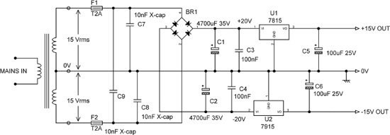
There are really only two electrical design decisions to be made; the AC voltage of the transformer secondary and the size of the reservoir capacitors. As to the first, you must make sure that the unregulated supply is high enough to prevent the rails dropping out (i.e. letting hum through) when a low mains voltage is encountered, but not so high that either the maximum input voltage of the regulator is exceeded or it suffers excessive heat dissipation. How low a mains voltage it is prudent to cater for depends somewhat on where you think your equipment is going to be used, as some parts of the world are more subject to brown-outs than others. You must consider both the minimum voltage drop across the regulators (typically 2 V) and the ripple amplitude on the reservoirs, as it is in the ripple troughs that the regulator will first “drop out” and let through unpleasantness at 100 Hz.
In general, the RMS value of the transformer secondary will be roughly equal to the DC output voltage.
The size of reservoir capacitor required depends on the amount of current that will be drawn from the supply. The peak-to-peak ripple amplitude is normally in the region of 1 to 2 volts; more ripple than this reduces efficiency, as the unregulated voltage has to be increased to allow for unduly low ripple troughs, and less ripple is usually unnecessary and gives excessive reservoir capacitor size and cost. The amount of ripple can be estimated with adequate accuracy by using Equation 22.1:
22.1 |
where:
- Vpk-pk is the peak-to-peak ripple voltage on the reservoir capacitor.
- I is the maximum current drawn from that supply rail in Amps.
- Δt is the length of the capacitor discharge time, taken as 7 milliseconds.
- C is the size of the reservoir capacitor in microfarads.
- The “1000” factor simply gets the decimal point in the right place.
Note that the discharge time is strictly a rough estimate and assumes that the reservoir is being charged via the bridge for 3 ms and then discharged by the load for 7 ms. Rough estimate it may be, but I have always found it works very well.
The regulators must be given adequate heatsinking. The maximum voltage drop across each regulator (assuming 10% high mains) is multiplied by the maximum output current to get the regulator dissipation in watts, and a heatsink selected with a suitable thermal resistance to ambient (in °C per watt) to ensure that the regulator package temperature does not exceed, say, 90 °C. Remember to include the temperature drop across the thermal washer between regulator and heatsink.
Under some circumstances it is wise to add protective diodes to the regulator circuitry, as shown in Figure 22.2. The diodes D1, D3 across the regulators are reverse-biased in normal operation, but if the power supply is driving a load with a large amount of rail decoupling capacitance, it is possible for the output to remain higher in voltage than the regulator input as the reservoir voltage decays, and this can damage the regulator. D1, D3 prevent this effect from putting a reverse voltage across the regulators.
The shunt protection diodes D2, D4 are once again reverse-biased in normal operation. D2 prevents the +15 V supply rail from being dragged below 0 V if the −15 V rail starts up slightly faster, and likewise D4 protects the −15 V regulator from having its output pulled above 0 V. This can be an important issue if rail-to-rail decoupling such as C9 is in use; such decoupling can be useful because it establishes a low AC impedance across the supply rails without coupling supply rail noise into the ground, as C7, C8 are prone to do. However, it also makes a low-impedance connection between the two regulators. D2, D4 will prevent damage in this case but leave the power supply vulnerable to start-up problems; if its output is being pulled down by the −15 V regulator, the +15 V regulator may refuse to start. This is actually a very dangerous situation, because it is quite easy to come up with a circuit where start-up will only fail one time in 20 or more, the incidence being apparently completely random but presumably controlled by the exact point in the AC mains cycle where the supply is switched on and other variables such as temperature, the residual charge left on the reservoir capacitors, and the phase of the moon. If even one start-up failure event is overlooked or dismissed as unimportant, then there is likely to be serious grief further down the line. Every power supply start-up failure must be taken seriously.

Designing a ±17 V Supply
There are 15 V IC regulators (7815, 7915), and there are 18 V IC regulators (7818, 7918), but there are no 17 V IC regulators. This problem can be effectively solved by using 15 V regulators and adding 2 volts to their output by manipulating the voltage at the REF pin. The simplest way to do this is with a pair of resistors that divide down the regulated output voltage and apply it to the REF pin, as shown in Figure 22.3a (the transformer and AC input components have been omitted in this and the following diagrams, except where they differ from those shown earlier). Since the regulator maintains 15 V between the OUT and REF pin, with suitable resistor values the actual output with respect to 0 V is 17 V.
The snag with this arrangement is that the quiescent current that flows out of the REF pin to ground is not well controlled; it can vary between 5 and 8 mA, depending on both the input voltage and the device temperature. This means that R1 and R2 have to be fairly low in value so that this variable current does not cause excessive variation of the output voltage, and therefore power is wasted.
If a transistor is added to the circuit as in Figure 22.3b, then the impedance seen by the REF pin is much lower. This means that the values of R1 and R2 can be increased by an order of magnitude, reducing the waste of regulator output current and reducing the heat liberated. This sort of manoeuvre is also very useful if you find that you have a hundred thousand 15 V regulators in store, but what you actually need for the next project is an 18 V regulator, of which you have none.
What about the output ripple with this approach? I have just measured a power supply using the exact circuit of Figure 22.3b, with 2200 uF reservoirs, and I found −79 dBu (87 uVrms) on the +17 V output rail and −74 dBu (155 uVrms) on the 17 V rail, which is satisfyingly low for inexpensive regulators and should be adequate for almost all purposes; note that these figures include regulator noise as well as ripple. The load current was 110 mA. If you are plagued by ripple troubles, the usual reason is a rail decoupling capacitor that is belying its name by coupling rail ripple into a sensitive part of the ground system, and the cure is to correct the grounding rather than design an expensive ultra-low ripple PSU. Note that doubling the reservoir capacitance to 4400 uF only improved the figures to −80 dBu and −76 dBu respectively; just increasing reservoir size is not a cost-effective way to reduce the output ripple.

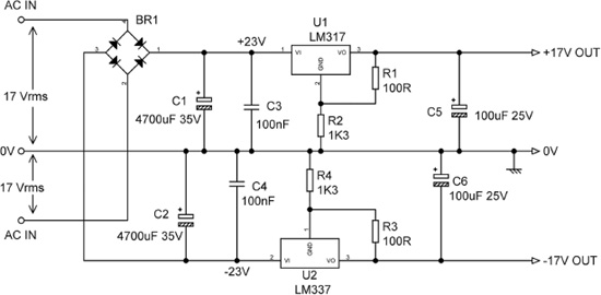
Using Variable-Voltage Regulators
It is of course also possible to make a ±17 V supply by using variable output voltage IC regulators such as the LM317/337. These maintain a small voltage (usually 1.2 V) between the OUTPUT and ADJ (shown in figures as GND) pins and are used with a resistor divider to set the output voltage. The quiescent current flowing out of the ADJ pin is a couple of orders of magnitude lower than for the 78/79 series, at around 55 uA, and so a simple resistor divider gives adequate accuracy of the output voltage, and transistors are no longer needed to absorb the quiescent current. A disadvantage is that this more sophisticated kind of regulator is somewhat more expensive than the 78/79 series; at the time of writing they cost something like 50% more. The 78/79 series with transistor voltage-setting remains the most cost-effective way to make a non-standard-voltage power supply at the time of writing.
It is clear from Figure 22.4 that the 1.2 V reference voltage between ADJ and out is amplified by many times in the process of making a 17 V or 18 V supply; this not only increases output ripple but also output noise, as the noise from the internal reference is being amplified. The noise and ripple can be considerably reduced by putting a capacitor C7 between the ADJ pin and ground. This makes a dramatic difference; in a test PSU with a 650 mA load, the output noise and ripple were reduced from −63 dBu (worse than the 78xx series) to −86 dBu (better than the 78xx series), and so such a capacitor is usually fitted as standard. If it is fitted, it is then essential to add a protective diode D1 to discharge C7, C8 safely if the output is short-circuited, as shown in Figure 22.5.

|
|
7815 + transistor |
LM317 |
|---|---|---|
|
No C on LM317 ADJ pin |
−73 dBu (all ripple) |
−63 dBu (ripple & noise) |
|
47 uF on LM317 ADJ pin |
−73 dBu(all ripple) |
−86 dBu (ripple & noise) |
|
Input filter 2.2 Ω & 2200 uF |
−78 dBu (ripple & noise) |
−89 dBu (mostly noise) |
|
Input filter 2.2 Ω & 4400 uF |
−79 dBu (mostly noise) |
−90 dBu (all noise) |
The ripple performance of the aforementioned test PSU, with a 6800 uF reservoir capacitor and a 650 mA load, is summarised for both types of regulator in Table 22.3. Note that the exact ripple figures are subject to some variation between regulator specimens.
Improving Ripple Performance
Table 22.3 shows that the best noise and ripple performance that can be expected from a simple LM317 regulator circuit is about −86 dBu (39 uVrms), and this still contains a substantial ripple component. The reservoir capacitors are already quite large at 4700 uF, so what is to be done if lower-ripple levels are needed? The options are:
- Look for a higher-performance IC regulator. They will cost more, and there are likely to be issues with single sourcing.
- Design your own high-performance regulator using discrete transistors or opamps. This is not a straightforward business, especially if all the protection that IC regulators have is to be included. There can be distressing issues with HF stability.
- Add an RC input filter between the reservoir capacitor and the regulator. This is simple and pretty much bullet-proof and preserves all the protection features of the IC regulator, though the extra components are a bit bulky and not that cheap. There is some loss of efficiency due to the voltage drop across the series resistor; this has to be kept low in value, so the capacitance is correspondingly large.
The lower two rows of Table 22.3 show what happens. In the first case the filter values were 2.2 Ω and 2200 uF. This has a −3 dB frequency of 33 Hz and attenuates the 100 Hz ripple component by 10 dB. This has a fairly dramatic effect on the visible output ripple, but the dB figures do not change that much, as the input filter does not affect the noise generated inside the regulator. Increasing the capacitance to 4400 uF sinks the ripple below the noise level for both types of regulator.
Dual Supplies From a Single Winding
It is very convenient to use third-party “wall-wart” power supplies for small pieces of equipment, as they come with all the safety and EMC approvals already done for you, though admittedly they do not look appropriate with high-end equipment.
The vast majority of these supplies give a single AC voltage on a two-pole connector, so a little thought is required to derive two supply rails. Figure 22.6 shows how it is
done in a ±18 V power supply; note that these voltages are suitable only for a system that uses 5532s throughout. Two voltage-doublers of opposite polarity are used to generate the two unregulated voltages. When the incoming voltage goes negative, D3 conducts and the positive end of C1 takes up approximately 0 V. When the incoming voltage swings positive, D1 conducts instead, and the charge on C1 is transferred to C3. Thus the whole peak-to-peak voltage of the AC supply appears across reservoir capacitor C3. In the same way, the peak-to-peak voltage, but with the opposite polarity, appears across reservoir C4.
Since voltage-doublers use half-wave rectification, they are not suitable for high current supplies. When choosing the value of the reservoir capacitor values, bear in mind that the discharge time in Equation 22.1 above must be changed from 7 ms to 17 ms. The input capacitors C1, C2 should be the same size as the reservoirs.

Mutual Shutdown Circuitry
The 5532 opamp is in general a tough item, but it has an awkward quirk. If one supply rail is lost and collapses to 0 V, while the other rail remains at the normal voltage, a 5532 can under some circumstances get into an anomalous mode of operation that draws large supply currents, and it ultimately destroys itself by over-heating. Other opamps may suffer the same problem, but I am not currently aware of any. To prevent damage from this cause opamp supplies should be fitted with a mutual shutdown system. This ensures that if one supply rail collapses because of overcurrent, over-temperature, or any other cause, the other rail will be promptly switched off. A simple way to implement this is shown in Figure 22.7, which also demonstrates how to make a ± supply using only positive regulators. Two separate transformer secondary windings are required; a single centre-tapped secondary cannot be used.
The use of a second positive regulator to produce the negative output rail looks a little strange at first sight, but I can promise you it works. The regulators in this case are the high-current Linear Tech LT1083, which can handle 7.5 amps but is not available in a negative version. That should be more than enough current for even the most complex active crossover …

The extra circuitry to implement mutual shutdown is very simple; R5, D3, R6 and Q1 and Q2. Because R5 is equal to R6, D3 normally sits at around 0 V in normal operation. If the +17 V rail collapses, Q2 is turned on by R6, and the REF pin of U2 is pulled down to the bottom rail, reducing the output to the reference voltage (1.25 V). This is not completely off, but it is low enough to prevent any damage to opamps.
If the −17 V rail collapses, Q1 is turned on by R5, pulling down the REF pin of U1 in the same way. Q1 and Q2 do not operate exactly symmetrically, but it is close enough for our purposes.
Note that this circuit can only be used with variable output voltage regulators, because it relies on their low reference voltages to achieve what is effectively switch-off.
Power Supplies for Discrete Circuitry
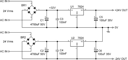
One of the main reasons for using discrete audio electronics is the possibility of handling larger signals than can be coped with by opamps running off ±17 V rails. The use of ±24 V rails allows a 3 dB increase in headroom, which is probably about the minimum that justifies the extra complications of discrete circuitry. A ±24 V supply can be easily implemented with 7824/7924 IC regulators.
A slightly different approach was used in my first published preamplifier design. [1] This preamp in fact used two LM7824 +24 V positive regulators, as shown in Figure 22.8, because at the time the LM7924 −24 V regulator had not yet reached the market. This configuration can be very useful in the sort of situation where you have a hundred thousand positive regulators in the stores but no negative regulators.
Note that this configuration does however require two separate transformer secondary windings; it cannot be used with a single centre-tapped secondary.