
Chapter 23
An Active Crossover Design
Here I present an active crossover design which will illustrate a good number of the principles and techniques put forward in this book. A design that demonstrated all of them would be a cumbersome beast, so I have aimed instead to show the most important while also providing a practical and adaptable design which will be of use in the real world.
The design is a generic crossover that can be adapted to a wide range of applications by changing its parameters and its configuration. The crossover frequencies can be changed simply by altering component values, and circuit blocks for equalisation or time delay can be added or removed, with due care to preserve absolute phase, of course. Since widely varying drive units may be used, I have made no attempt to specify equalisation or integrate the driver response into the filter operation.
The crossover design is primarily aimed at hi-fi applications rather than sound reinforcement. It does not, for example, in its basic form have variable crossover frequencies or balanced outputs, though instructions are given for adding the latter.
Design Principles
The aim of this chapter is not just to provide a complete design but to demonstrate the use of various design principles expounded in the body of this book.
• |
Low-impedance design for low noise |
|
• |
Elevated internal levels |
|
• |
Further elevated internal level for the HF path |
|
• |
Low-noise balanced inputs |
|
• |
Optimised filter order for best noise |
|
• |
Mixed-capacitor types in filters |
|
• |
Use of multiple resistors to improve accuracy |
|
• |
Delay compensation using 3rd-order allpass filters |
Example Crossover Specification
This is the basic specification for an active crossover that we will use as an example.
Number of bands: |
Three |
Type |
Linkwitz-Riley 4th-order |
Mid/HF crossover frequency: |
3 kHz |
LF/Mid crossover frequency: |
400 Hz |
HF path time-delay compensation |
80 usec, tolerance ±5 % (path length 27 mm) |
Mid path time-delay compensation |
400 usec, tolerance ±5 % (path length 137 mm) |
(As noted in Chapter 13, the path lengths to be compensated for were carefully chosen to give nice round figures for the delay times required.)
The crossover has balanced inputs, but in its basic form the outputs are unbalanced, the assumption being that if a balanced interconnection is required, this will be provided at the power amplifier inputs. The possibility of adding balanced output stages is examined at the end of the chapter. If the overall audio system can be satisfactorily designed with balanced crossover inputs but unbalanced crossover outputs, as opposed to unbalanced crossover inputs but balanced crossover outputs, then the former is clearly more economical, as for a stereo crossover it requires two balanced input stages rather than six balanced output stages.
Low-impedance design is used throughout; the circuit impedances are designed to be as low as possible without causing extra distortion by overloading opamp outputs. This reduces the effect of opamp current noise and resistor Johnson noise but has no effect on opamp voltage noise.
The design assumes that there is no level control between the crossover and power amplifier, or if there is, it is set to maximum and left there; this allows us to use elevated internal levels in the crossover to improve the noise performance, as described in Chapter 17.
No equalisation stages are included in the signal paths.
The block diagram is shown in Figure 23.1.
The Gain Structure
In Chapter 17 I explained how with suitable system design the internal levels of an active crossover could be significantly raised to reduce the effect of circuit noise. Here I have decided to go for an internal level of 3 Vrms, 12 dB higher than the assumed input voltage of 775 mVrms (0 dBu). This retains 10 dB of headroom to accommodate maladjusted input levels. We also saw in Chapter 17 that the distribution of amplitude with frequency in music is such that the levels in the top few octaves are much lower than in the rest of the audio spectrum. We decided conservatively that with an upper crossover point around 3 kHz, it was safe to raise the HF channel level by a further 6 dB.
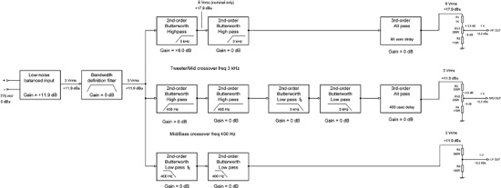
It is therefore necessary to have an input amplifier with a gain of close to four times (+11.9 dB) to raise the internal level to a nominal 3 Vrms as soon as possible, and another +6 dB of amplification will be required as early as possible in the HF path.
The bandwidth definition filter is shown in Figure 23.1 as having unity gain for simplicity at this point. In fact, as we shall shortly see, it has a small loss of 0.29 dB, which has to be recovered elsewhere in the circuitry to keep the levels spot-on.
Resistor Selection
The basic policy for component selection is that followed throughout this book—to use as few capacitors as possible, which means sticking to the sparse E3 or E6 series, and let the resistor values come out as they may. I decided that no more than two resistors from the E24 series would be used in series or parallel to get as close as possible to the desired value. Where it could be done the resistors would be of near-equal value to get the best possible improvement in accuracy by using multiple resistors, as explained in Chapter 15. An error window for the nominal value is set at ±0.5%, and 1% tolerance resistors are assumed.
Resistors in parallel rather than in series are generally to be preferred, as it makes the PCB layout easier; assuming they are lying side by side, you just have to join the adjacent pads with very short tracks. It could also be argued that the parallel connection makes for better reliability, as a dry solder-joint that develops into an open circuit is less likely to cause oscillation or stop the signal altogether. In some sound-reinforcement circumstances, any sound is better than none at all.
Capacitor Selection
I decided to use polypropylene capacitors wherever they would have a measurable effect on the performance. They get bulky and expensive quickly as their value increases, and so I further concluded that 220 nF should be the largest value employed. It is assumed that only the E3 series (10, 22, 47) values are available. The number of different capacitor values (not counting small ceramics) has been kept down to four: 2n2, 10 nF, 47 nF and 220 nF. It makes sense to put some effort into this, as they are probably the most expensive electronic components in the crossover, and so you want to gain as much cost advantage from purchasing in quantity as possible. No particular assumptions are made about capacitor tolerance.
The Balanced Line Input Stage
It was explained in Chapter 20 that the conventional unity-gain balanced input stage made with four 10 kΩ resistors is relatively noisy, especially when compared with an unbalanced input using a simple voltage-follower; the balanced stage noise output is about −104.8 dBu. This problem can be addressed by reducing the value of the 10 kΩ resistors around the balanced stage and driving the balanced stage with 5532 unity-gain buffers to keep the input impedance up. In the unity-gain case this reduces the noise output to −110.2 dBu, a very useful 5.4 dB quieter.
For our crossover design we do not want a unity-gain stage but one that gives a gain of 4 times (+11.9 dB) so that a nominal input of 775 mVrms is raised to 3 Vrms. We use the same strategy of input buffers and a balanced amplifier working at low impedances, but the required gain is obtained by altering the ratio of the resistors R7, R8 to R9, R10 in Figure 23.2. The output noise from this stage with the inputs terminated by 50 Ω resistors is −100.9 dBu, so its equivalent input noise (EIN) is −100.9 − 11.9 = −112.8 dBu. For what it’s worth, this is the same as the Johnson noise from a 9.6 kΩ resistor.
This is a rare case where a significant amount of gain is required in a balanced input amplifier, so the instrumentation amplifier configuration might be an interesting alternative, giving a CMRR theoretically improved by 11.9 dB, the gain of the stage.
The Bandwidth Definition Filter
The bandwidth definition stage is a combined filter consisting of a 3rd-order Butterworth highpass with a cutoff frequency of 20 Hz to remove subsonic signals and protect loudspeakers and a 2nd-order Butterworth lowpass with cutoff at 50 kHz. Unlike the example in Chapter 8, E24 resistor values have been used in the subsonic section to get the cutoff frequency exactly at 20 Hz. The physically large 220 nF capacitors in the filter are susceptible to electrostatic hum pickup, and this must be considered in the physical layout of the crossover.
The bandwidth definition filters are placed as early as possible in the signal path, immediately after the balanced input amplifier, to prevent headroom being eaten up by large subsonic signals. This should also minimise the generation of intermodulation distortion by large ultrasonic signals.
The combined filter has a small midband loss of −0.29 dB when designed with 220 nF capacitors. Redesigning it to use 470 nF capacitors (keeping the capacitors in the lowpass section the same) would reduce this to an even more negligible loss of−0.15 dB, but it’s hard to argue that the result is worth the significant extra cost of the capacitors. The only real problem with the 0.29 dB loss is that when tracking a test signal through the HF path, you will encounter 2.90 Vrms at the combined filter output, instead of a nice round 3.0 Vrms. Rather than propagate this inelegance through the rest of the HF path, the signal is restored to 3.0 Vrms in the next stage. This attenuate-then-amplify process inevitably incurs a noise penalty, but in this case it is very small indeed. If an extra stage was used to recover the loss, this would be inelegant and uneconomic, but since the next stage in the HF path is already configured to give gain, there is no cost penalty at all.
The HF Path: 3 kHz Linkwitz-Riley Highpass Filter
The HF signal path in Figure 23.3 includes two 2nd-order Butterworth filters that make a 4th-order Linkwitz-Riley filter. Both are of the Sallen & Key type. The first filter is configured for a gain of +6.29 dB, to raise the nominal level to make the signal less vulnerable to circuit noise and also to recover that 0.29 dB loss in the combined filter. The nominal level in the block diagram of Figure 23.1 is shown as “6 Vrms”, which if it was a real level would be too high, but the relatively low amount of HF energy in musical signals gives a level of more like 3 Vrms in practical use. A level of 6 Vrms will however be obtained if you apply a signal at 775 mVrms to the input, given a suitably high frequency above the MID-HF crossover point.

The design of this stage is straightforward—see Chapter 8 for more information on designing Sallen & Key filters with whatever gain you want. The value of R20 comes very conveniently as the E24 preferred value of 1k3, but the value of the second resistance in the filter comes out as 970.7 Ω, well away from either 910 Ω or 1 kΩ. R2 is therefore made up of a parallel pair R21 and R22. The optimal method for selecting these was described in Chapter 15. If the two resistors are approximately equal in value, the accuracy of their combined resistance is improved by a factor of √2, as the errors tend to cancel. Thus a 1% tolerance becomes a 0.707% tolerance. As the values become more unequal, the improvement decreases until it is effectively 1%, as the tolerance is decided by only one resistor. The procedure is therefore to start with near-equal values and pick a resistor pair to give a result just above the target value, and then pick a resistor pair to give a result just below. If neither result is within the desired error window, one of the resistors is incremented, and we try again. As this algorithm proceeds, the resistor values become more and more unequal and the improvement in tolerance diminishes, so the sooner we find a satisfactory answer the better. In some respects you have to balance the improvement in tolerance against the accuracy of the combined resistance value obtained. The process is mechanical and tedious and would be best implemented in some procedural programming language, but once set up on a spreadsheet, it is fairly quick to do.
In this case our target value is 970.7 Ω and the error window is ±0.5%. Our progress is set out in Table 23.1; as Step 1 we start with 1800 Ω in parallel with 2000 Ω, the combined resistance of which is 2.4% low. The next value above 2000 Ω is 2200 Ω, which with 1800 Ω gives a combined resistance 1.99% high. Our target value is therefore irritatingly about halfway between these two resistor combinations. In each step we find the two resistor values that “bracket” the target: in other words one value gives a combined resistance that is too low and the other a combined resistance that is too high.
Step 2: We reduce the 1800 Ω resistor to 1600 Ω and try again. Putting 2400 Ω in parallel gives a combined resistance that is only 1.1% low, our best shot so far, but nowhere near good enough. Putting 2700 Ω in parallel gives a result 3.5% high. Are we downhearted? Yes, but faint heart never built fair crossover, so we will persist.
Step 3: We reduce the 1600 Ω resistor to 1500 Ω and find that 2700 Ω in parallel is only 0.66% low, which is temptingly close to 0.5%, but there is no point in setting error windows if you’re not going to stick to them. We proceed, but with the nagging awareness that each step is reducing the accuracy improvement we will get from using multiple resistors.
Step 4: Reduce the 1500 Ω resistor to 1300 Ω and with 3600 Ω in parallel the result is 1.61% low. However, with 3900 Ω in parallel, bingo! The combined value is only 0.44%, inside our ±0.5% error window, but not, it must be said, a very long way inside it.
Our task is done. Or is it? There is always the nagging doubt that you might get a much better result if you go just a step or two further. In this case that doubt is very much justified.
Step 5: Reduce the 1300 Ω resistor to 1200 Ω, and with 4700 Ω in parallel the result is 1.52% low. But with 5100 Ω in parallel—cracked it! The result is only 0.08% high and more than good enough, considering the tolerance of the components. The accuracy improvement is much impaired, as one resistor is more than four times the other, but the 1300 Ω and 3900 Ω resistor combination in Step 4 is not much better in that respect.
We therefore select R21 as 1200 Ω and R22 as 5100 Ω. I realise that this process sounds a bit long-winded when every step is described, but a spreadsheet version is quick and convenient. I should warn you at this point that the Goalseek function in Excel apparently can’t cope with the mathematical expression for the value of parallel resistors and tends to unhelpfully offer “solutions” up in the peta-ohm regions. However, this doesn’t slow things down much; just don’t use it.
|
Step |
R21 Ohms
|
R22 Ohms
|
Combined Ohms
|
Error %
|
|---|---|---|---|---|
|
1 |
1800 |
2000 |
947.368 |
−2.40% |
|
|
1800 |
2200 |
990.000 |
1.99% |
|
2 |
1600 |
2400 |
960.000 |
−1.10% |
|
|
1600 |
2700 |
1004.651 |
3.50% |
|
3 |
1500 |
2700 |
964.286 |
−0.66% |
|
|
1500 |
3000 |
1000.000 |
3.02% |
|
4 |
1300 |
3600 |
955.102 |
−1.61% |
|
|
1300 |
3900 |
975.000 |
0.44% |
|
5 |
1200 |
4700 |
955.932 |
−1.52% |
|
|
1200 |
5100 |
971.429 |
0.08% |
The next step is to check by calculation or simulation (not measurement because the tolerances of the real components used will confuse things) that the filter cutoff frequency falls within the required error window.
In The Case of the Second Filter (Quick, Watson, the game’s afoot!) we are much luckier. Using the process just described, we find that taking the value of the first resistor as 800 Ω gives an error of −0.23% in the filter cutoff frequency, which is less than the resistor tolerance (even after the full √2 accuracy improvement, which we get in this case) and probably much less than the capacitor tolerances. Thus R26 and R27 are 1k6, and R28 is also 1k6. It happens to work out very nicely, though in terms of component count we only save one resistor.
In each filter, only the first capacitor (C20, C22) is a polypropylene type, while the second (C21, C23) is polyester. Only one capacitor needs to be polypropylene to avoid capacitor distortion, but it must be the first one in the filter. This intriguing state of things is described more fully in Chapter 11.
The HF Path: Time-Delay Compensation
When we looked at the question of time-delay compensation in Chapter 13, we noted that mercifully it is not necessary to maintain an absolutely accurate delay over the whole audio spectrum. Instead the delay only has to be constant over each crossover region. The HF delay needs only to be maintained around the 3 kHz crossover point for so long as both drive units are radiating significantly, and likewise the MID delay needs only to be constant around the 400 Hz crossover. One of the many advantages of the Linkwitz-Riley crossover configuration is that the slopes are steep at 24 dB/octave, and so these regions of overlap are relatively narrow, simplifying the problem.
When allpass filters are used as delay elements they give a constant group delay at low frequencies, but it begins to fall off at high frequencies. This makes the design of the HF delay more complicated than that of the MID delay. A 1st-order allpass filter designed for a delay of 80 usec unfortunately starts to roll-off quite early; as frequency rises the delay is down by 10% at 2.4 kHz, before we even reach the 3 kHz crossover point, and sinks to 50% at 9.3 kHz, slowly approaching zero above 100 kHz. A 1st-order allpass filter clearly won’t do the job.
One solution is to cascade three 1st-order filters in series. The delay is now spread out over three sections, with each one set to a 80 usec/3 = 26.7 usec delay. The total 80 usec delay is now sustained up to three times the frequency, being 10% down at 7.5 kHz and not down 50% until 28 kHz, well outside the audio spectrum. So is this good enough? The MID and HF drivers will be contributing equally at 3 kHz, both of them being 6 dB down. While 7.5 kHz is only 1.3 octaves away from the 3 kHz MID-HF crossover frequency, the high slope of the Linkwitz-Riley crossover means that the signal to the MID drive unit will be 32 dB down, though its acoustical contribution is less certain, as it depends on the driver frequency response.
Another solution would be a 2nd-order allpass filter; the delay of an 80 usec version falls by 10% at 4.79 kHz, better than the 1st-order filter (10% down at 2.5 kHz) but worse than the triple 1st-order filter (10% down at 7.2 kHz). The 2nd-order filter as described in Chapter 13 also has the disadvantage of phase-inverting in the low-frequency range where its delay is constant. It is also 3.2 dB noisier than the 3rd-order solution we are about to look at. All in all, a 2nd-order allpass filter does not look promising.
The last delay filter examined in detail in Chapter 13 is the 3rd-order allpass filter, which is made up of a 2nd-order allpass cascaded with a 1st-order allpass. When designed for an 80 usec delay, it is 10% down at 12.7 kHz, giving almost twice the flat-delay frequency range of the three cascaded 1st-order filters, at a fractionally lower cost, as it actually uses one less resistor. It uses the same number of potentially expensive capacitors. The −10% point for the delay is now 2.1 octaves above our 3 kHz crossover frequency, and the signal sent to the MID driver will be down by 50 dB, so whatever the response of the driver itself we can be pretty sure that the fall-off in time delay will have no audible consequences. When designed for 80 usec, it is 3.2 dB quieter than the equivalent 2nd-order filter, and it does not inconveniently phase-invert in the low-frequency range. The 3rd-order filter is clearly the better solution, and so it is chosen for the HF path delay.
The 80 usec 3rd-order allpass filter is studied in detail in Chapter 13, with full consideration of its quite subtle noise and distortion characteristics, so I will not repeat that here. Suffice it to say that the circuit of Figure 13.22 is cut and pasted into our schematic in Figure 23.3. In the MFB filter, both capacitors are polypropylene, though the mixed-capacitor phenomenon applies to MFB filters as well as Sallen & Key filters, as described in Chapter 11.
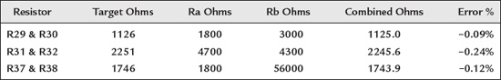
The parallel resistor combinations for the awkward resistance values in the HF allpass filter are given in Table 23.2. We will get a good improvement in precision with R31 and R32, as the values are near equal, not much for R29 and R30, and virtually none for R37 and R38, where our luck was right out.
The schematic of the complete HF path is shown in Figure 23.3. Note that the component numbering starts at 20 for resistors and capacitors and 10 for opamps; this is to allow additions to other parts of the schematic without renumbering everything. The signal and noise levels are given for the output of each stage.
The allpass stage can of course be omitted if time-delay compensation is done by other means, such as the physical cabinet construction.
The MID Path: Topology
The MID path contains a 400 Hz 4th-order Linkwitz-Riley highpass filter and a 3 kHz 4th-order Linkwitz-Riley lowpass filter. In this situation the order of the filters in the signal path needs to be considered. In Chapter 17 I demonstrated that a noise advantage can be gained by putting the lowpass filter second in the path, as it removes some of the noise from the previous highpass filter. With the filter frequencies we are using here, the noise advantage is 1.1 dB; not an enormous amount, but achieved at no cost whatsoever. Let’s do it.

You will recall that in the HF path the first filter was configured to give +6.3 dB of gain, recovering the 0.3 dB loss in the bandwidth definition filter. While it would be possible to configure the first MID filter to give +0.3 dB of gain (we do not want the +6.0 dB in this path), it does not seem worth the extra complication as +0.3 dB represents only a very small change in the position of the output level control.
The MID Path: 400 Hz Linkwitz-Riley Highpass Filter
The MID path begins with two 400 Hz 2nd-order Butterworth highpass filters that make a 4th-order Linkwitz-Riley highpass filter. Both are of the unity-gain Sallen & Key type, since there is no need for gain, and in fact they are identical.
We might have been lucky with the resistor values of the second filter in the HF path, but things pan out differently here. The target value for the exact 400 Hz cutoff frequency is 1278.9 Ω. That is temptingly close to 1300 Ω, but shoving that value in alone gives a cutoff frequency error of −1.6%; clearly we could simply add quite a high value in parallel to tweak the resistance just a little, but there will be effectively no improvement in accuracy. Perhaps there are two more nearly equal values that will give the combined value we want? Regrettably not. Playing the combinations, we find that the first pair of values that puts the cutoff frequency within the ±0.5%. error window is R50 = 1300 Ω in parallel with R51 = 82 k Ω, so that’s what we have to use. The error in the cutoff frequency is only −0.07%.
The second resistance in the filter has a target value of 1278.9 Ω times two, which is 2557.7 Ω. Our first attempt at a parallel combination is R52 = 5100 Ω in parallel with R53 = 5100 Ω, which gives 2550 Ω, which is only 0.30% low. Looks like there’s no need to need to look any further. And yet there is the nagging doubt that there might be a better solution … and there is. The very next step is 5600 Ω in parallel with 4700 Ω, giving 2555.3 Ω, which is only 0.09% low and still gives us almost all the accuracy improvement possible. In this case there is not much point in looking further yet. The same resistor values are used in both filters.
As for the filters in the HF path, only the first capacitors (C50, C52) need to be polypropylene for low distortion; the second capacitors (C51, C53) can be polyester.
The MID Path: 3 kHz Linkwitz-Riley Lowpass Filter
After the 400 Hz highpass filter come the two 2nd-order Butterworth lowpass filters that make up a 4th-order Linkwitz-Riley lowpass filter. Both are of the unity-gain Sallen & Key type. Using 47 nF capacitors, the target value for the two resistors is 798.15 Ω. We can see at once that two 1600 Ω resistors in parallel is going to be very close, and the combined resistance of 800 Ω is in fact only 0.23% low. We also get the maximum possible improvement in accuracy, so we look no further.
The MID Path: Time-Delay Compensation
The time delay required in the MID path is five times longer at 400 usec, but on the other hand it covers the 400 Hz crossover point, so the delay does not need to be constant up to such a high frequency. Let’s see if that makes thing any easier.
Since a 1st-order allpass filter designed for a delay of 80 usec has the delay down by 10% at 2.4 kHz, we would expect the same filter designed for a 400 usec delay to be down by 10% at 480 Hz, and simulation confirms that this is so; the relationship is just simple proportion. Because 480 Hz is much too close to the 400 Hz crossover point, once more we are going to have to look at a more sophisticated solution. We will aim for 10% down at two octaves above crossover, in other words at 1.6 kHz, because this gave pretty convincing results in the HF path.
Looking at the options, we can say that: Three 1st-order filters in series will be 10% down at 7.5 kHz/5 = 1.5 kHz. This is 1.9 octaves away from crossover and is very close to our target, but this configuration uses a relatively large number of components. Four cascaded 1st-order filters would certainly do the job, but the component count is looking excessive compared with the other options, because four capacitors and four opamp sections are required, while the 3rd-order allpass filter only uses three of each.
A 2nd-order allpass filter designed for 400 usec will be down 10% at 4.79 kHz/5 = 958 Hz. This is not even close to our two-octave target, and, as we have seen, the 2nd-order allpass filter has performance issues compared with the 3rd-order, and an unwanted phase-inversion. We can rule this approach out.
A 3rd-order allpass filter designed for 400 usec will be 10% down at 12.7 kHz/5 = 2.54 kHz, and simulation confirms this figure is correct. It is 2.7 octaves away from crossover and gives us a healthy safety margin—in fact it looks almost a bit too healthy, as all the evidence is that a two-octave spacing is ample. However, it is the only alternative that meets our requirements, and there is no obvious way to save a few parts by cutting the spacing down a bit. It is therefore once more selected for our design.
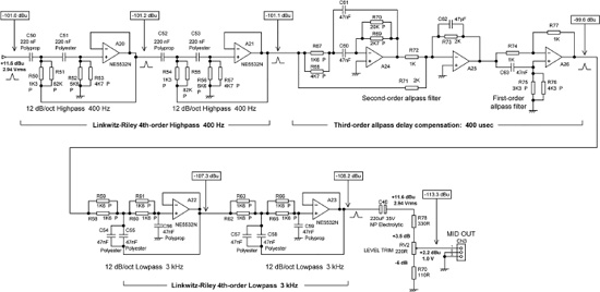
The 400 usec 3rd-order allpass filter is very similar to that of the 80 usec version in the HF path, the main difference being that the capacitors have increased from 10 nF to 100 nF and the resistor values adjusted accordingly to get the desired delay time. The schematic of the complete MID path is shown in Figure 23.4. Note that the component numbering starts at 50 for resistors and capacitors and 20 for opamps; this is to allow additions to other parts of the schematic without renumbering everything. The signal and noise levels are given for the output of each stage.
The parallel resistor combinations for the three non-preferred resistance values in the MID allpass filter are given in Table 23.3. We will get a reasonable improvement in precision with R67 and R68, as the values are near equal, not much for R75 and R76, and virtually none for R69 and R70.
The allpass stage can be omitted if time-delay compensation is done by alternative means, such as the physical construction of the enclosure.
The LF Path: 400 Hz Linkwitz-Riley Lowpass Filter
The LF path is the simplest of the three paths in the crossover. It consists of two 400 Hz 2nd-order Butterworth lowpass filters that make a 4th-order Linkwitz-Riley lowpass filter. Both are of the unity-gain Sallen & Key type. The target resistance value for the two resistors is 1278.9 Ω, which not surprisingly is the same value as the first resistor in the MID highpass filter, as both use a capacitance value of 220 nF. As before, the first pair of values that puts the cutoff frequency within the ±0.5%. error window is 1300 Ω in parallel with 82 k Ω. The error in the cutoff frequency is only −0.07%.


The LF Path: No Time-Delay Compensation
No time-delay compensation is required in the LF path because the physical distance between the acoustic centres of the LF and MID drive units is compensated for by the delay in the MID path. In fact, if the delay compensation was in the LF path, it would have to have a negative delay; in other words the output would emerge before the input arrived. Such circuits, though they would be extremely useful for predicting lottery numbers if you wired enough in series, are notoriously hard to design.
The schematic of the complete LF path is shown in Figure 23.5. The component numbering starts at 80 for resistors and capacitors and 40 for opamps to allow additions to other parts of the schematic without renumbering. The signal and noise levels are given for the output of each stage.
Output Attenuators and Level Trim Controls
The output level controls used here have a deliberately limited range because they are not intended to be used as volume controls. The range about the nominal 1 Vrms output is +3.5 dB to −6.0 dB, and this should be more than enough to allow for power amplifier gain tolerances (assuming a nominally identical set of power amplifiers) or drive unit sensitivity variations. If, however, the crossover is intended to work with a wide range of power amplifiers of varying sensitivities, the range may need to be extended by reducing the end-stop resistors at the top and bottom of the preset control.

The values chosen give the nominal output with the preset wiper central in its track, so the system can be lined up pretty well just by eye; this won’t of course work with multi-turn preset pots. The exactness of this unfortunately depends on the track resistance of the preset in relation to the fixed end-stop resistors above and below it, and the tolerance on these components is unlikely to be better than 10%, and it may be 20%. These tolerances are horribly wide compared with the 1% of fixed resistors. If really precise levels are required, the output will have to be measured during the trimming operation.
The output networks are configured with the lowest possible resistances that will not load the opamp upstream excessively, to keep the final output impedance low enough to drive a reasonable amount of cable without HF losses. The assumption in this design is that the power amplifiers will not be too far away, and their inputs will be driven directly. Putting a unity-gain buffer after the level trim network would allow a lower output impedance, especially if the “zero-impedance” type of buffer is used, but this will compromise the noise performance.
An alternative approach would be to reduce the resistor values in the output networks so the maximal output impedance is as low as desired and then drive this with a suitable number of 5532 unity-gain buffers connected in parallel via 10 Ω current-sharing resistors. The impairment of the noise performance due to another amplifier stage will in this case be negligible, especially since the noise contributions of the added buffers will partially cancel as they are uncorrelated. You might however need to keep an eye on the power dissipation in the output network resistors, especially the preset.
An unbalanced output will give better common-mode rejection if it is configured as impedance-balanced, by using a three-pin output connector with the cold (−) pin connected to ground through an impedance that approximates as closely as possible to the output impedance driving the hot (+) output pin. This improves the balance of the interconnection, as fully described in Chapter 20. In our circumstances here the output impedance of the level trim network varies as the wiper of the preset is moved from one end of its travel to the other, and so the impedance from the cold pin to ground is inevitably a compromise.
In the case of the HF path, the output impedance varies from 248 Ω with the trimmer at maximum and 101 Ω with the trimmer at minimum. The middle setting, which gives the nominal output level, gives an output impedance of 184 Ω. An impedance-balance resistor of 180 Ω will give negligible common-mode error.

The MID path output impedance varies from 165 Ω at maximum to 92 Ω at minimum, with a middle value of 147 Ω, so an impedance-balance resistor of 150 Ω will give a very small error.
The LF path has no output level trim, and its output impedance is fixed at 120 Ω, so here the impedance-balancing can be made exact. The impedance-balanced outputs for the three paths are shown in Figure 23.6.
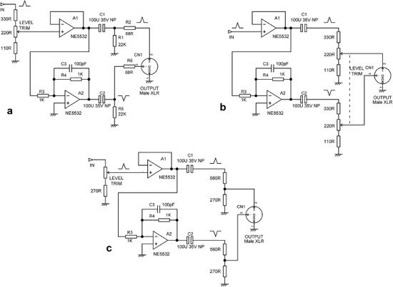
Balanced Outputs
In the domestic applications for which this crossover is intended, it is doubtful if any real advantages will be gained by adding true balanced outputs. If placed after the output attenuator and trim networks, as in Figure 23.7a, they will compromise the noise performance, while if placed before the output networks, as in Figure 23.7b, a dual-gang trim-pot is required; good luck with sourcing that. A solution to this dilemma is to separate the gain trim and output attenuation functions, as shown in Figure 23.7c.
If the prospective power amplifiers have unbalanced inputs, consideration should be given to the possibility of using ground-cancelling outputs, as described in Chapter 21.
Crossover Programming
Many of the resistors in the schematics in this chapter have the letter “P” next to their resistance value. These are the components that need to be altered to change the characteristics of the crossover. The idea is that these resistor positions on a prototype PCB can be fitted with single-way turned-pin sockets like those that ICs are plugged into. It is then possible to very easily plug resistors in and out during the development of the complete crossover-loudspeaker system. This is much quicker than pulling the PCB out of the case, desoldering one resistor and then re-soldering another one in, and PCBs will only take so much of this before the pads are damaged. When the design is finalised, the PCBs will have resistors soldered into the same positions in the usual way.
Single-pin sockets can be obtained by cutting up a strip of sockets. Make sure you use the kind of socket strip intended for this sort of thing—deconstructing IC sockets does not usually work well, as the plastic is more brittle and tends to shatter.
Noise Analysis: Input Circuitry
The schematics of the input circuitry, the HF path, the MID path, and the LF path all have the measured noise levels at the output of each stage indicated by rectangular boxes with arrows. This information is essential for performing a noise analysis, in which the noise contribution of each stage is assessed to see if it is what we expect and how it relates the noise generated by the other stages in the path we are examining. Because of the way that uncorrelated noise sources add in a RMS fashion, the largest noise source tends to dominate the final result—the noise at the end of the path—and so we want to identify that source and see if it is worthwhile to make it quieter and so improve the overall noise performance.
As throughout this book, all the noise measurements given are unweighted and in a 22 kHz bandwidth.
The measured noise output from the balanced input stage with its +11.9 dB of gain is −100.9 dBu. When we terminate both input pins with 50 Ω to ground, the Johnson noise from each resistor is −135.2 dBu (22 kHz bandwidth at 25°C). The noise from both together is 3 dB more, not 6 dB, because the two noise sources are uncorrelated. The noise voltage at the input is thus a very very low −132.2 dBu. When amplified by +11.9 dBu this becomes −120.3 dBu, which is almost 20 dB below the stage output noise and is therefore making a negligible contribution to the total. Despite its special low-noise design, virtually all the output noise is generated by the balanced input amplifier.
The equivalent input noise (EIN) of the balanced input stage is −100.9 dBu − 11.9 dB = −112.8 dBu, giving us a noise figure of 22.4 dB with reference to 50 Ω. This figure would usually be considered pretty poor, but as is discussed in Chapter 20 on line inputs, noise figures are not a very useful figure of merit for balanced inputs. What is unquestionably true is that −100.9 dBu is a very low value of noise to find in audio circuitry, so we seem to have made a good start.
The noise level at the output of the bandwidth definition filter might be expected to be a bit higher, because of its noise contribution, but it is actually a tad lower, at −101.0 dBu. This is because of the lowpass action of the filter. If the 22 kHz measurement filter was a brickwall job this would not happen, but it has in fact only a 18 dB/octave roll-off, so the bandwidth definition filtering above 22 kHz does have enough effect to outweigh the noise contribution of the stage.
At this point we cannot say that either stage is in urgent need of improvement, though we note that effectively all the output noise from the input circuitry is generated internally by the balanced input amplifier.
Noise Analysis: HF Path
The measured noise output from the input circuitry and the first 3 kHz highpass filter is −95.1 dBu. This filter has a gain of +6.3 dB, and the noise level at its input is −101.0 dBu, so if the stage was noiseless we would expect a noise output of −101.0 dBu + 6.3 dB = −94.6 dBu; in fact the measured noise output is less than this, at −95.1 dBu. This is of course because we are dealing with a 3 kHz highpass filter which is rejecting a substantial chunk of the audio spectrum. Calculating the noise contribution from this stage is therefore quite complicated. For the moment we will simply note that this stage does not appear to be excessively noisy.
The measured noise output from the second 3 kHz highpass filter is −95.2 dBu. This filter has a gain of 0 dB, but again the output noise level is fractionally less than the input noise, due to the filtering action.
The final stage in the HF path is the 80 usec 3rd-order allpass filter time-delay compensator, which we might expect to be relatively noisy compared with the filters because of its greater complexity. However, the noise at its output is only 0.2 dB higher than at its input, measuring −95.0 dBu. If we subtract the input noise from the output noise we get an estimate for the stage contribution of −108.5 dBu; unfortunately, we are subtracting two figures with only a small difference between them. That difference is fairly near the limit of measurement, and so the result will be very inaccurate. If you want to know the noise from a stage, then the correct method is to measure the noise output of the stage by itself. We did this for the 3rd-order allpass filter back in Chapter 13, and the actual output noise was −102.8 dBu, which shows you how dangerous it is to use the subtraction method inappropriately. If we add the internal noise of −102.8 dBu to the input noise of −95.2 dBu, in theory we get an output noise of −94.5 dBu, an increase of 0.7 dB (the small discrepancy is probably due to minor frequency response irregularities in the allpass filter caused by capacitor tolerances). We make a note that the noise contribution of the 3rd-order allpass filter is small but not negligible. More importantly, we can conclude that the noise performance of the HF path is dominated by the noise being fed to it from the input circuitry.
The final part of the HF path is the output attenuator and level trim network, which at its nominal setting has a 15.6 dB loss to undo the doubly-elevated level in the HF path. Since it is just a resistive attenuator, I expected no problems here. But … the noise level measured at the network output was −105.1 dBu, when it should have been −95.0 dBu −15.6 dBu =−110.6 dBu. A 5 dB discrepancy cannot be ignored; investigation showed that the problem was the output impedance of the network, which at 184 Ω is somewhat higher than usual. The Audio Precision SYS-2702 is designed to be fed from low-impedance sources, and one might conclude that its input amplifiers have relatively high current noise as a consequence of attaining very low voltage noise, but Bruce Hofer assures me this is not so. [1] Nevertheless, I found that driving the AP input via a 5532 unity-gain buffer and the usual 47 Ω cable-isolating resistor, to reduce the source impedance, gave a lower output noise reading of −109.4 dBu, despite the extra amplifier in the path. This minor puzzle remains unresolved at present.
In any event, I hope can all agree that is −109.4 dBu is pretty quiet.
Noise Analysis: MID Path
The measured noise output from the first unity-gain 400 Hz highpass filter is −101.2 dBu. This is again less than the input noise because of the filtering action. The measured noise output from the second unity-gain 400 Hz highpass filter is −101.1 dBu, a tiny increase at the limit of measurement. We conclude that neither filter is making a significant contribution to the noise in the MID path.
After the two highpass filters come the two 3 kHz lowpass filters, fed with −101.1 dBu of noise from the second 400 Hz highpass filter. The noise output from the first lowpass filter is −108.6 dBu, and from the second lowpass filter −109.4 dBu. Both these figures are much lower than the input noise of −101.1 dBu as a consequence of the lowpass filtering, which cuts the bandwidth from 22 kHz to 3 kHz.
The final stage in the MID path, as in the HF path, is a 3rd-order allpass filter time-delay compensator, this time designed for a 400 usec delay. We saw when we looked at the HF allpass filter in isolation that it was relatively noisy, with a measured output noise of −102.8 dBu; in this case the different circuit values for 400 usec give us a slightly lower allpass-filter-only noise output of −104.1 dBu (the 2nd-order allpass filter that makes up the first section of the complete 3rd-order filter has a noise output of −104.9 dBu, so that is clearly where most of the noise comes from). When the 3rd-order allpass filter is placed in the MID path, the measured noise output is −102.9 dBu. Since this is more than 6 dB greater than the −109.4 dBu noise level going in, it is clear that by far the greater part of the noise is internally generated by the 3rd-order allpass filter. This is because the nominal level in the MID path is 6 dB lower than that in the HF path. We make a note that the noise contribution of the 3rd-order allpass filter is dominant and might repay some attention.
The final part of the MID path is the output attenuator and level trim network, which at its nominal setting has a 9.5 dB loss to undo the elevated level in the MID path. The noise level measured directly at its output was initially −107.9 dBu, but as we saw at the end of the HF path, that reading is exaggerated by the AP input current noise. Driving the AP input via a 5532 unity-gain buffer and 47 Ω cable-isolating resistor reduced the output noise reading to −110.4 dBu. That too, is rather quiet; the noise level is lower than that at the HF path output because of the presence of the 3 kHz lowpass filters.
Noise Analysis: LF Path
This path consists only of the two 400 Hz lowpass filters and the fixed output attenuator. Given the 400 Hz cutoff frequency of the lowpass filters we expect a good noise performance, and we get it. The noise at the input of the LF path is the −101.0 dBu coming from the input circuitry. This is reduced to −111.0 dBu at the output of the first lowpass filter, and further to −112.2 dBu at the output of the second lowpass filter.
The final part of the LF path is the fixed output attenuator network, which has a 9.5 dB loss to undo the elevated level in the MID path. This in theory gives an output noise of −121.7 dBu. This is going to be hard to measure, as it is below the noise floor of the AP measuring equipment, which is, on my example, −119.6 dBu with the input short-circuited. Once more we have to drive the AP input via a 5532 unity-gain buffer and 47 Ω cable-isolating resistor to avoid misleadingly high readings due to current noise, and that 5532 will add its own voltage noise. The reading we get is −113.8 dBu. This is reduced to −115.1 dBu after we subtract the known AP noise floor. We then calculate the noise added by the 5532 buffer, as it is too low to measure accurately, using its typical input noise density of 5 nV/√Hz and a 22 kHz bandwidth (the effect of the 5532 current noise in the attenuator output impedance is negligible). The answer is that the 5532 buffer contributes −120.38 dBu. If we subtract that from our figure of −115.1 dBu, we get a stunningly low −116.6 dBu. This may not be the most accurate reading in the history of audio, but it is good evidence that everything is working properly, and we have a very low noise output from the LF path.
Improving the Noise Performance: The MID Path
On our journey down the MID path, we noted that the 3rd-order allpass filter time-delay compensator was generating internally most of the noise that was measured at its output. It is the dominant noise generator in the MID path, so let’s see if we can do something about that.
There is a very simple fix, which you may have already seen coming. The 3rd-order allpass filter is at the end of the MID path, so all its noise heads for the output unmolested. If, however, it is moved so it is after the 400 Hz highpass filters but before the 3 kHz lowpass filters, the latter will have a dramatic effect on the noise level. Making the change, the noise output of the 3rd-order allpass filter is now −99.6 dBu as it adds its own noise to the −101.1 dBu reaching it from the highpass filters upstream. The noise output of the first lowpass filter is pleasingly lower at −107.3 dBu, and the noise output of the second lowpass filter is even lower at −108.2 dBu.
After the output attenuator network, the noise at the output is reduced from −110.4 dBu to −113.3 dBu, an improvement of 2.9 dB that costs us nothing more than a moment’s thought.
The true noise output must be −108.2 −9.5 dBu = −117.7 dBu, because of the effect of the 9.6 dB output attenuator, but we have already described the difficulties of measuring noise at such low levels. The revised schematic is shown in Figure 23.8.
In case you’re wondering why the MID path wasn’t configured in this way from the start, the answer is that until I built the prototype circuit, I didn’t know how the noise contributions of the stages was going to work out. It could have been predicted by a lot of calculation, but that gets complicated when you’re dealing with stages like filters that have a non-flat-frequency response. Sometimes it’s just quicker to get out the prototype board and start plugging bits in. You’re going to be doing it sooner or later.
Improving the Noise Performance: The Input Circuitry
The other major point we noted in our noise analysis of the crossover was that the noise performance of the HF path was dominated by the noise being fed to it from the input circuitry, the incoming level being −101.0 dBu. This is almost all coming from the balanced input amplifier, the contribution of the bandwidth definition filter being very small. Therefore the only way to improve things is to take a hard look at the balanced input amplifier; clearly our original design decision to make it a special low-noise type was sound, but what are the options for making it even quieter? Improvements to this stage are going to be value for money, as it will reduce the noise level being fed to all three signal paths.
Now, you might be questioning whether it is worth spending any more money at all on noise reduction, because the circuitry is already extremely quiet, and you might expect the equipment upstream, the preamplifier, mixing console, or whatever, to generate a higher noise level than the crossover. This to my mind is a matter of design philosophy rather than dogged pragmatism. We may suspect the source equipment may be noisier than our circuitry, but that is the responsibility of whoever designed it. If we make our device as good as we can without making obviously uneconomic decisions, then we not only get a virtuous warm glow, but we can be sure we are relatively future-proof in terms of improvements that may be brought about in the source equipment. There is also the point that we will get some excellent numbers for our specification, and they may impress prospective customers.
In Chapter 20 we looked at a series of improvements that could be made to unity-gain balanced input amplifiers to improve their noise performance, all of which, regrettably but perhaps inevitably, required more numerous or more costly opamps. Here we are dealing with a gain of +11.9 dB, so the optimal path of improvement may be somewhat different. The balanced input stage consists of two unity-gain buffers and a low-impedance balanced (differential) amplifier. From here on I shall just refer to them as “the buffers” and “the balanced amplifier”. Given the difficulty of measuring the very low noise levels at the outputs of the attenuator network, the noise was measured just before the attenuator and the output noise calculated. In each case the input noise of the AP measuring system has been subtracted in an attempt to obtain accurate numbers.
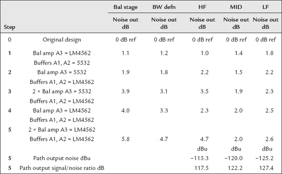
We proceed as follows: Step 1: Replace the 5532 opamp A3 in the balanced amplifier with the expensive but quiet LM4562. This gives a rather disappointing reduction in the noise from the balanced stage of 1.1 dB, which feeds through to even smaller improvements in the path outputs
Step 2: We deduce that the input buffers A1, A2 must be generating more of the noise than we thought, so we put the 5532 back in the A3 position and replace both input buffers with a LM4562; since the LM4562 is a dual opamp, this makes layout simple. The noise from the balanced stage is now 1.9 dB better than the original design, which is more encouraging, and two of the paths have a 2.2 dB improvement. This sounds impossible but actually results from the three crossover paths dealing with different parts of the audio spectrum. At any rate there is no doubt that the modification of Step 2 is more effective than Step 1.
Step 3: We enhance the balanced amplifier by putting two identical 5532 stages in parallel and averaging their outputs by connecting them together with 10 Ω resistors. The LM4562 input buffers are retained, as their superior load-driving capability is useful for feeding two balanced stages in parallel. This drops the balanced input stage noise to 3.9 dB below the original design. The improvement at the output of the bandwidth definition filter is less at 3.1 dB. The filter makes its own noise contribution, and this is now more significant. Once more there are lesser but still useful reductions in the noise out from the three paths.
Step 4: LM4562s are not cheap, but we decide to splurge on two of them. We return to a single balanced amplifier using an LM4562, and the LM4562 input buffers are retained. This is very little better than Step 3 and significantly more expensive.
Step 5: It appears that abandoning the double balanced amplifier was not a good move, so we bring it back, this time with both of its sections employing an LM4562. This gives a very definite improvement, with the balanced input stage noise now 5.8 dB below the original design. The path output noise measurements also improve, though by a lesser amount, because, like the bandwidth definition filter, the noise generated by the path circuitry has become more significant as the noise from the balanced input stage has been reduced. We have only replaced two opamp packages with the LM4562 (which is about ten times more costly than the 5532), so the cost increase is not great.
The reduction in balanced input amplifier noise could be pursued much further by more extensive paralleling of opamps, as described in Chapter 20. However, is it worthwhile? This is questionable given the noise that is generated downstream of it.
These results are summarised in Table 23.4, together with their effect on the noise output (before the output attenuator) of each of the three crossover paths. You will note a few minor inconsistencies in the last decimal place of some of the figures; this is due partly to the fact that the three paths are handling different parts of the audio spectrum and to some extent due to the difficulties of measuring the very low noise levels accurately. Nonetheless, the overview it gives of the worth of the various modifications is correct.
Looking at the bottom two rows of the table which gives the final noise outputs and the signal/noise ratios for a 1 Vrms output (after the output attenuators), we can see that the HF path is the noisiest by a long way, despite its 6 dB higher internal level. This is because it contains a relatively noisy 3rd-order allpass filter but no lowpass filters to discriminate against noise. Clearly that 6 dB extra level is a very good idea. The MID path is quieter because it does have a lowpass filter which can be placed after its 3rd-order allpass filter. The LF path consists only of a lowpass filter and is consequently the quietest of the lot.

The final version (Step 5) of the input circuitry is shown in Figure 23.9. Note that the bandwidth definition filter has not been modified in any way.
The Noise Performance: Comparisons With Power Amplifier Noise
The noise performance of this active crossover, especially after the modifications, is, I hope you will agree, rather good. But how does it compare with the noise from a well-designed power amplifier? The EIN of a Blameless power amplifier is −120 dBu [2] if the input signal is applied directly to the power amplifier rather than through a balanced input stage. As we have seen, balanced input stages are relatively noisy and are much noisier than a power amplifier alone.
The figure of −120 dBu is therefore the most demanding case to compare the crossover noise against. What are we trying to achieve? If we accept that the noise from the loudspeakers can go up by 3 dB when we connect the crossover, its output noise must be no more than −120 dBu, at the same level as the power amplifier EIN. If however we are more demanding and will only stand for a noise increase of 1 dB, which is at the limit of audibility, then the crossover output noise must be reduced to −126 dB. We will take that figure as a target and see what can be done.
We will look at the noise output of the MID path, because the ear is most sensitive in this part of the audio spectrum (400 Hz–3 kHz). The noise output after the performance optimisation is −120.0 dBu. This is very quiet indeed for a piece of audio equipment but regrettably 6.0 dB higher than the ambitious target we have just adopted. You may be doubting if the crossover noise performance could be improved that much, and while I am sure it could be done, I am less sure that it could be done economically.
The resistance values in the crossover have already been reduced as much as possible without introducing extra distortion or demanding large and expensive capacitors, thus reducing the effects of opamp current noise and resistor Johnson noise, but this has no effect on opamp voltage noise. The effect of this can only be reduced by using more expensive opamps with a lower input voltage noise density or by paralleling opamp stages. Neither technique promises a radical reduction in noise when practically applied.
Nonetheless, let us conduct a thought experiment. We know that whatever amplifier technology you use, putting two amplifiers in parallel and averaging their outputs (usually by connecting them together with 10 Ω resistors) reduces the noise output by 3 dB; putting four in parallel reduces the noise by 6 dB; and so on. The same applies to putting two identical active crossovers in parallel, so … if we stacked up four of them, we could unquestionably get a 6 dB noise reduction and meet our target. This is perhaps not very sensible, but it does prove one thing—it is physically possible to perform the formidable task of meeting our demanding noise target, even if it is hardly economical to do so.
Conclusion
The description of this active crossover has hopefully demonstrated the techniques and design principles described in this book. The use of elevated internal levels, plus other low-noise techniques, has allowed us to achieve a remarkable noise performance.