
In the preceding chapters, we looked at various communication protocols, such as UART, SPI, and I2C. In this chapter, we cover JTAG, which is a bit different from what we have seen so far, and is not exactly a communication protocol. JTAG is a widely misunderstood concept, even within the security community.
The Joint Test Action Group (JTAG) is an association created in the mid-1980s when a group of companies came together to solve the problem of debugging and testing chips while dealing with the increasing complexity of devices.
During that period, embedded device manufacturers realized the trouble in traditional bed of nails testing was with the new assembled PCBs, due to increasing device density, especially while working with chips having an extremely high number of pins. Imagine the manual effort needed to test hundreds of chips with multiple pins in each of them and testing whether each of them is working well and communicating properly. To overcome this problem, the manufacturers came up with a standard that allows them to embed a piece of hardware into the chip itself to allow easier testing of various pins present in different chips of the PCB. This methodology was standardized by the IEEE in 1990 and named IEEE 1149.1.
JTAG is not a standard or protocol, but rather just a way of testing different chips present on the device and debugging them. JTAG uses a technique known as boundary scan, which enables manufacturers to test and diagnose the assembled PCBs with much greater ease compared to the old traditional approach.
Boundary Scan
As just mentioned, boundary scan is a technique to debug and test various pins of the different chips present in a circuit. This is done by adding a piece of component called boundary scan cells near each pin of the chip that needs to be tested. The various I/O pins of the device are connected serially to form a chain. This chain can then be accessed by what is called the test access port (TAP).
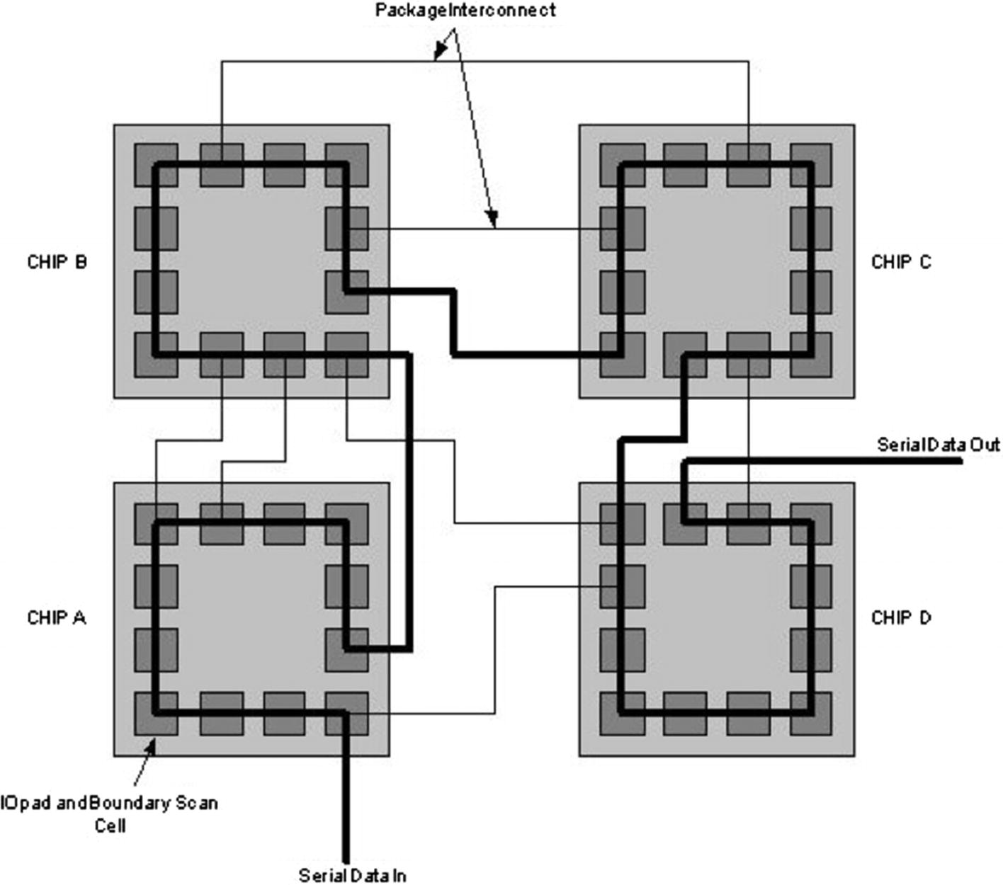
Describing boundary scan cells (Source: CMOS VLSI design: A circuits and systems perspective, 3rd ed., Neil H. E. Westw & David Harris)
Notice the I/O pads and the boundary scan cell near the periphery of each chip. These boundary scan cells can be accessed and checked for the values in the pins associated with the boundary scan cells. An external file known as a boundary scan description language file defines the capabilities of any single device’s boundary scan logic.
Test Access Port
Test clock (TCK): Used to synchronize the internal state machine operation and to clock serial data into the various boundary cells.
Test data in (TDI): The serial input data pin to the scan cells.
Test data out (TDO): Sends the serial output data from the scan cells.
Test mode select (TMS): Used to control the state of the TAP controller.
Test reset (TRST, optional): The reset pin that is active low. When it is driven low, it will reset the internal state machine.
The TCK, TMS, and TRST pins drive a 16-bit TAP controller machine that manages the overall exchange of data and instructions.
The TAP controller is a 16-stage finite state machine (FSM) that proceeds from state to state, based on the TMS and TCK signals. The TAP controller controls the test data register and the instruction register with the control signals. If an instruction is to be sent, then the clock (TCK) is activated and the reset is set to active low for the clock cycle. Once that is done, the reset signal is then deactivated and the TMS is toggled to traverse the state machine for further operation.
Boundary Scan Instructions
BYPASS: The BYPASS instruction places the BYPASS register in the DR chain, so that the path from the TDI and TDO involves only a single flip-flop (shift-resistor). This allows a specific chip to be tested in a serial chain without any overhead or interference from other chips.
SAMPLE/PRELOAD: The SAMPLE/PRELOAD instruction places the boundary scan register in the DR chain. This instruction is used to preload the test data into the boundary scan register (BSR). It is also used to copy the chip’s I/O value into the data register, which can then be moved out in successive shift-DR states.
EXTEST: The EXTEST instruction allows the user to test the off-chip circuitry. It is like SAMPLE/PRELOAD but also drives the value from the data register onto the output pads.
Test Process
The TAP controller applies test data on the TDI pins.
The BSR monitors the input to the device and the data are captured by the boundary scan cell.
The gata then go into the device through the TDI pins.
The data come out of the device through the TDO pins.
The tester can verify the data on the output pin of the device and confirm if everything is working.
These tests can be used to find things ranging from a simple manufacturing defect, to missing components in a board, to unconnected pins or incorrect placement of the device, and even device failure conditions.
Debugging with JTAG
Even though the JTAG was originally created to assist with eliminating the old bed of nails testing, in the new-age embedded development and testing world, it is used to perform several activities such as debugging the various chips present on the device, accessing individual pin values on each chip, overall system testing, identifying faulty components in a highly dense PCB, and so on. Because JTAG is available in the systems from the very start, as soon as the system boots up, it makes it extremely useful for testers and engineers to look at all the various components present in the embedded device.
For penetration testers and security researchers, it is extremely useful as it allows us to debug the target system and its individual components. This also means if our target board has JTAG access available and contains an onboard flash chip, we would be able to dump the contents from the flash chip via JTAG. We will also be able to set breakpoints and analyze the entire stack, instruction sets, and registers while debugging with JTAG, and integrating it with a debugger.
Now that you know how useful JTAG is going to be for us to identify vulnerabilities in the target device or perform security research, the next step would be to identify the JTAG pinouts present on the target device.
Identifying JTAG Pinouts
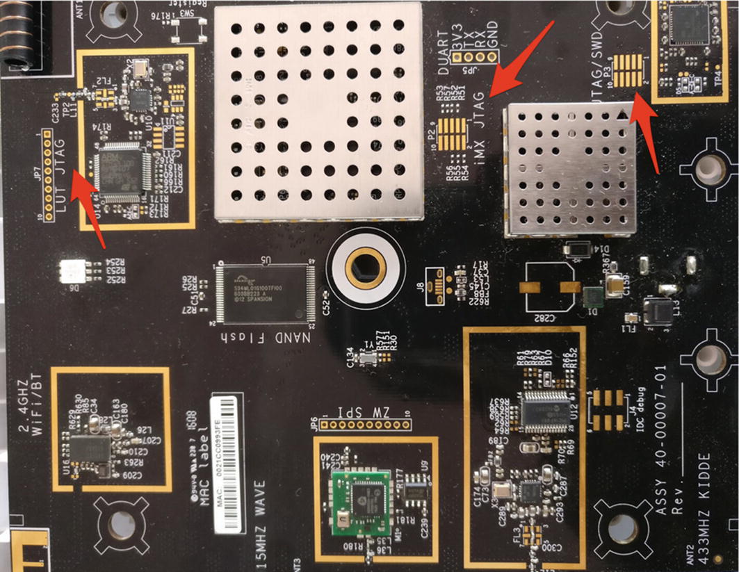
Identifying JTAG pinouts can be a bit trickier compared to UART, where all you would need is to look for a set of three or four pins and then use multimeter to identify the individual pinouts. In the case of JTAG, we will need to use additional tools (e.g., JTAGulator) to effectively determine the individual pinouts present in our target device.
In JTAG, we are concerned with usually four pins: TDI.
TDO.
TMS.
TCK.

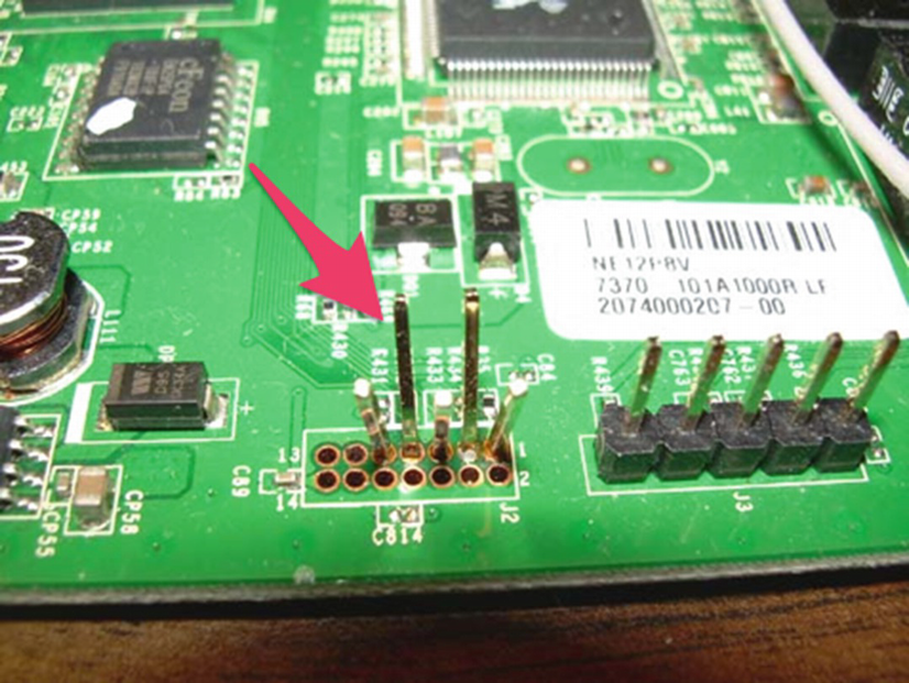
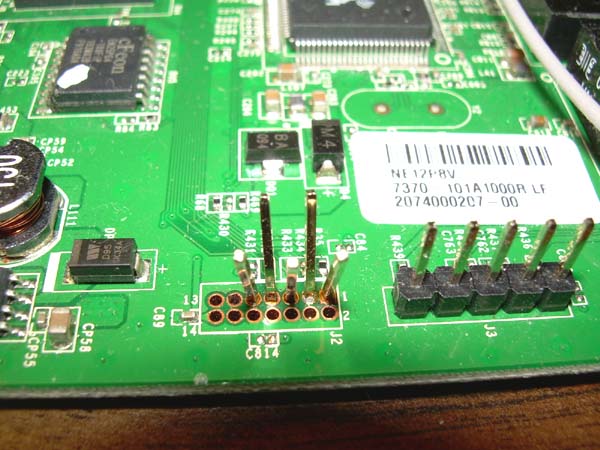
JTAG pinouts in Netgear WG602v3 (Source: https://www.dd-wrt.com/phpBB2/files/jtag_wg602v3_643.jpg )
JTAG interfaces on a Wink Hub
JTAG on a Linksys WRT160NL (Source: http://www.usbjtag.com/jtagnt/router/wrt160nljtag.jpg )
Figures 6-3 and 6-4 show the PCB image of Wink Hub and the different JTAG interfaces.
Now that you understand how JTAG pinouts might look on a real-world device, let’s go ahead and start identifying what the pinout is for the JTAG interface we have just found.
For this exercise, you can use any device with a JTAG interface. For starters, though, I would recommend choosing a development board that has a specified JTAG interface on it that could be used for debugging. Good examples are Raspberry Pi or Intel Galileo, both of which come with JTAG pins on them.
- 1.
Using JTAGulator.
- 2.
Using Arduino flashed with JTAGEnum.
Using JTAGulator
JTAGulator is open source hardware, designed by Joe Grand of Grand Idea Studios, which helps us identify JTAG pinouts for a given target device. It has 24 I/O channels that can be used for pinout discovery and can also be used to detect UART pinouts.
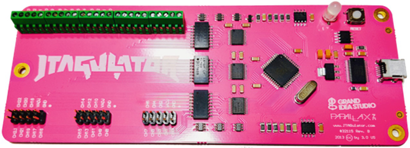
JTAGulator by Joe Grand
Once you’re on the JTAGulator screen, the next step would be to set the target system voltage by pressing V to select the target voltage.
After selecting the voltage, the next step is to select a BYPASS scan to find the pinouts. On selecting this, you will be required to specify how many channels you have selected for the pinouts.
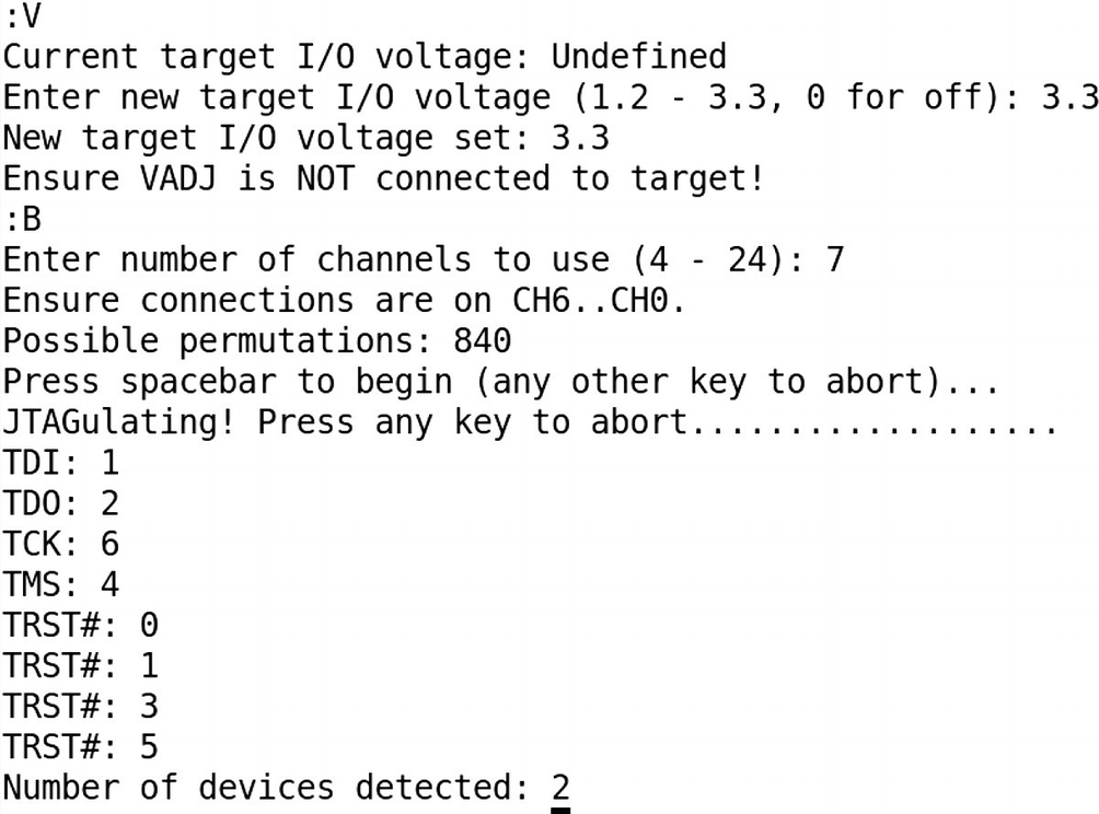
Detecting JTAG pinouts with JTAGulator
Based on which pins on your target device are connected to which channel, you will be able to identify the pinouts of the JTAG interface on the target device.
Using Arduino Flashed with JTAGEnum
Another popular technique of identifying JTAG interface is using Arduino. This is a much cheaper alternative compared to JTAGulator, but there are a few limitations, such as the scan being extremely slow and not having the ability to detect UART pinouts like JTAGulator does.
To use JTAGEnum with Arduino, the first step is to use the JTAGEnum program available at https://github.com/cyphunk/JTAGenum .
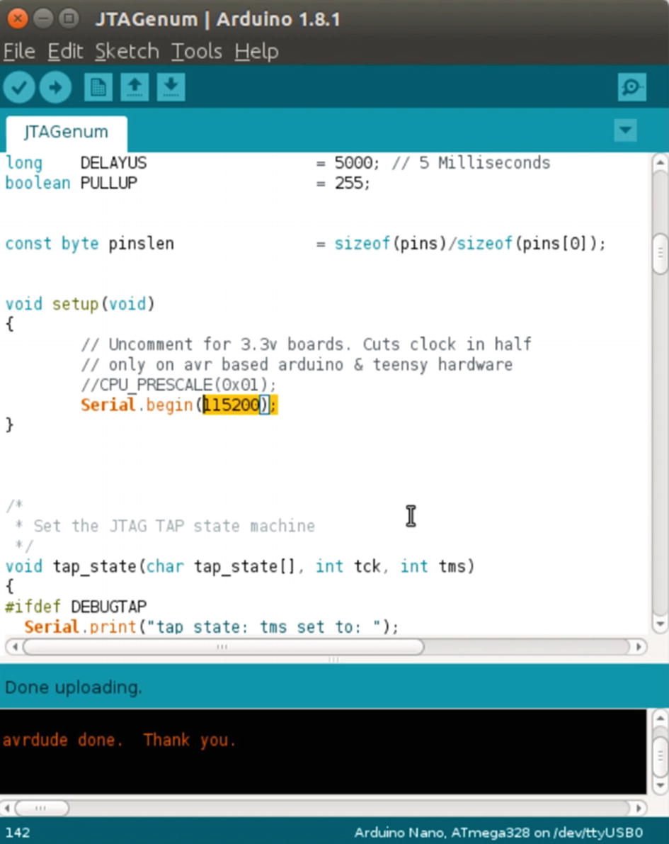
Arduino flashed with JTAGEnum to detect JTAG pins
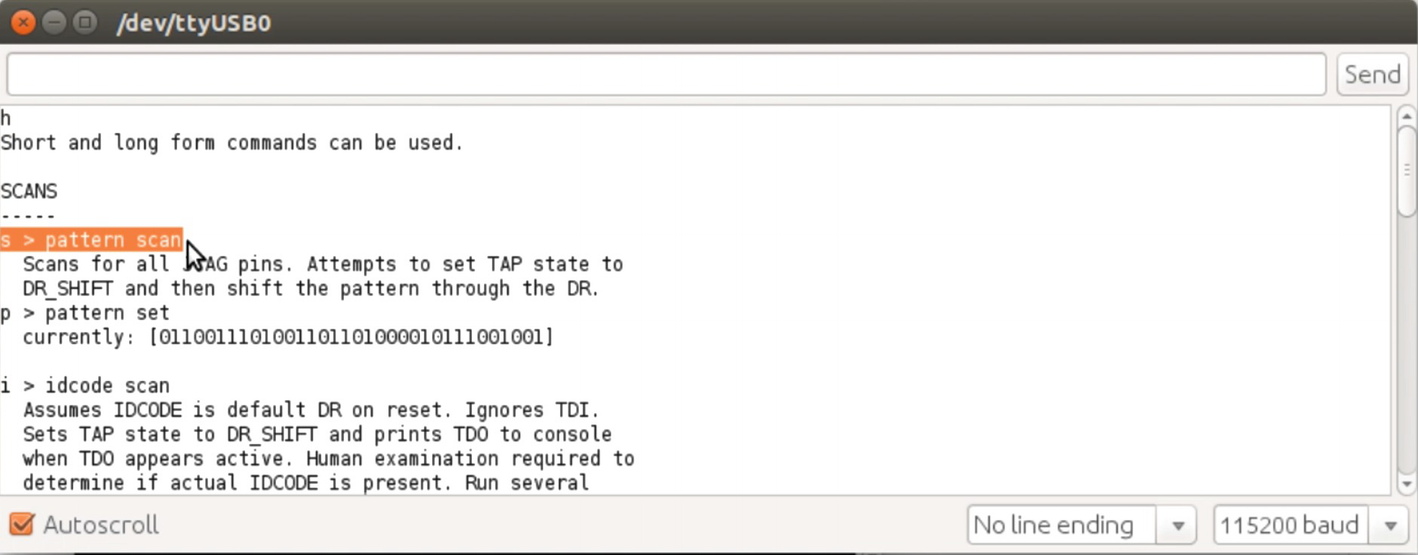
Moving forward with the scanning
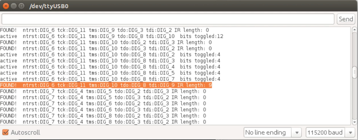
JTAGEnum was successful in detecting JTAG pinouts
Just like you did earlier, map those wires to the ones connected on the target device and you will have the actual JTAG pinouts of the target device.
Now that we have identified the JTAG pinouts of the target device, the next step is to connect to the JTAG interface and debug the target device and the programs running on it. For this, we need knowledge of OpenOCD, which is what we are going to be discussing in the next section.
OpenOCD
Debug the various chips present on the device.
Set breakpoints and analyze registers and stack at a given time.
Analyze flashes located on the device.
Program and interact with the flashes.
Dump firmware and other sensitive information.
OpenOCD, as you can see, is an extremely useful utility when we have to work with JTAG. In the next sections, we look at how we can set up OpenOCD and use it to perform additional exploitation of our target device.
Installing Software for JTAG Debugging
OpenOCD
GDB-Multiarch
Attify Badge tool
Once you have installed OpenOCD, we are ready to get started with our exploitation.
An additional useful utility to install here would be GDB-Multiarch, which would allow us to use GDB to debug binaries meant for different architectures, as most of the time we would be dealing with target devices and binaries that are not meant for the typical x86 architecture.
Alternatively, if you install the Attify Badge tool from https://github.com/attify/attify-badge and run install.sh, it will automatically install all the tools required for you, including OpenOCD. You can also use the AttifyOS located at https://github.com/adi0x90/attifyos , which is preconfigured with all the required tools.
Hardware for JTAG Debugging
Attify Badge or other tools such as BusPirate or Segger J-Link.
Target device with the JTAG interface.
For the sake of simplicity, we are using an Attify Badge for our JTAG debugging purposes. To use the Attify Badge with the target device, we will need to connect the corresponding JTAG pins of the device with the Attify Badge’s pinouts for JTAG, which we look at in the next section.
To make use of the Attify Badge (or any other hardware for that matter), we need the OpenOCD configuration file for it and the configuration file for the target device (and for any other devices in the chain). Here, the Attify Badge will work like a JTAG adapter, and the target device can either be a processor or a controller.
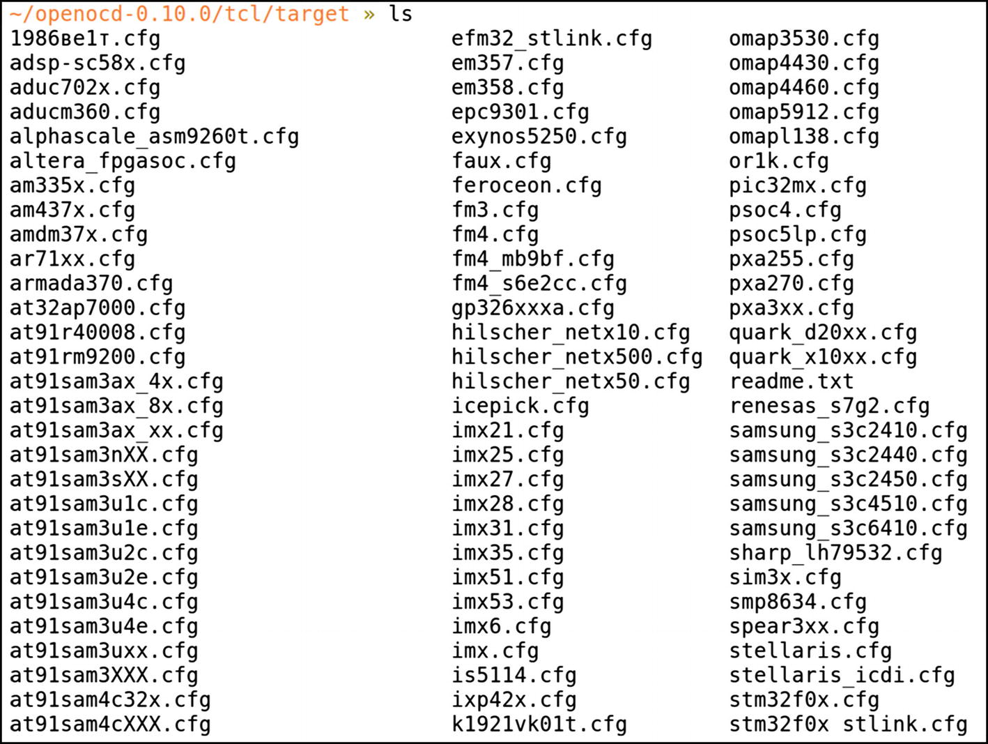
OpenOCD targets
You should always ensure that your target is listed in the OpenOCD targets, which come with the source, or else you will have to create a manual configuration file for your target device.
Setting Things up for JTAG Debugging
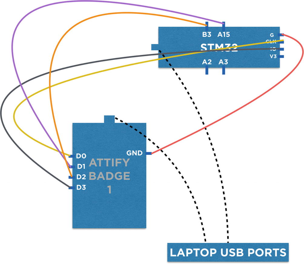
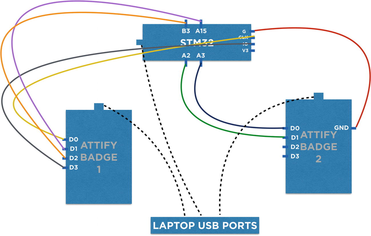
Connections for JTAG with Attify Badge
Pin on the Attify Badge | Function |
|---|---|
D0 | TCK |
D1 | TDI |
D2 | TDO |
D3 | TMS |
TCK (D0) goes to CLK of the target device.
TDI (D1) goes to TDI of the target device.
TDO (D2) goes to TDO of the target device.
TMS (D3) goes to TMS of the target device.
The pins functioning as CLK, TDI, TDO, and TMS would differ based on the processor or controller of the target device that you are trying to exploit.
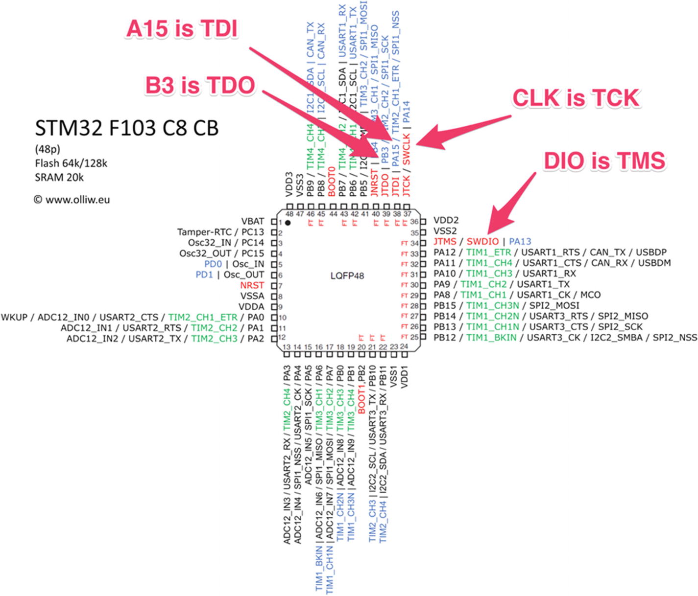
PIN configuration of STM32F103C8 microcontroller
Once the connections have been done, the next step would be to ensure that we have the configuration (.cfg) files for the Attify Badge, as well as for our target.
For the configuration file of our target, the STM32 microcontroller, we can get it from the OpenOCD configurations itself.
Connections for JTAG debugging
As we can see from that text, OpenOCD is able to connect to our target device and shows us additional information such as six breakpoints, four watchpoints, and more.
As you can see, we are able to connect to our target device and chip over JTAG using OpenOCD. This means that we were successful in identifying the correct JTAG pinouts and can now proceed with further exploitation of our target device.
Performing JTAG Exploitation
Now that you are successfully connected, at this point you can use the telnet session with OpenOCD and JTAG to write firmware to the microcontroller, debug binaries, and even dump firmware from it.
Let’s have a look at them one by one, starting with writing firmware to the device.
Writing Data and Firmware to a Device
The flash memory in this case starts at the address 0x08000000 and the current size of the contents at that address is 0x0, which indicates that the target device contains no firmware at present. We use the address from the previous output and pass it on to our next command specifying to write a custom-created firmware, firmware.bin. The firmware in this case enables authentication over UART for our target board.
This technique is useful when working with devices where you want to dump the contents from various flash chips, and even write malicious values to them.
Dumping Data and Firmware from the Device
If other techniques of obtaining the firmware fail, JTAG is our fallback option. We can use JTAG with the dump_image command to dump the firmware from the file system.
Reading Data from the Device
We can also selectively read data from specific memory addresses using JTAG. This is useful when we know the exact address that we want to read and later maybe modify.
Converting the value 61 74 74 69 66 79 from the output, which is in hex, to ASCII, we get the actual password, which in this case is attify. Similarly, we can also write a new value to the memory address to change the password the device uses for UART authentication.
This is a simple demonstration of how you can use reading contents from the memory to your advantage during exploitation. When performing it during your pentests, make sure to look for anything of potential interest, then figure out the address in hexdump or through a disassembler, and finally read and write values using JTAG debugging.
Debugging over JTAG with GDB
Often, you need to debug binaries and firmware over JTAG to understand the functionality in a much better way, and to modify some of the register values or instruction sets and change the program execution flow.
Now that we are already familiar with debugging using GDB, we will use GDB to debug a binary that we have flashed over JTAG. The binary can be downloaded from the code samples of the book available at https://attify.com/ihh-download . Once we have flashed the binary, we then proceed with debugging the binary runtime with JTAG and GDB.
Now you might be wondering how we can connect GDB to the target process over JTAG. The answer to that is whenever we run OpenOCD for a target to perform JTAG debugging, it also enables two different services, the first one being telnet over Port 4444, which we use to interact with OpenOCD, and the other being GDB over Port 3333, which we can use to debug binaries running on the target device.
Once you have the GDB for arm up and running, you can go ahead and set up breakpoints using either hbreak or the break to better analyze the binary and analyze the entire stack and registers when the breakpoint is hit. hbreak is used to set a hardware-assisted breakpoint, whereas break can be used to set a normal breakpoint at either an instruction, memory location, or function.
As we can see, verifypass is a function to compare the user input password to the actual password using the strcmp instruction at the address 0x080002e4. Based on the result, if the authentication is granted, it then branches to either 0x8000290 for dooropen or continues further if the passwords do not match.
JTAG connections with UART
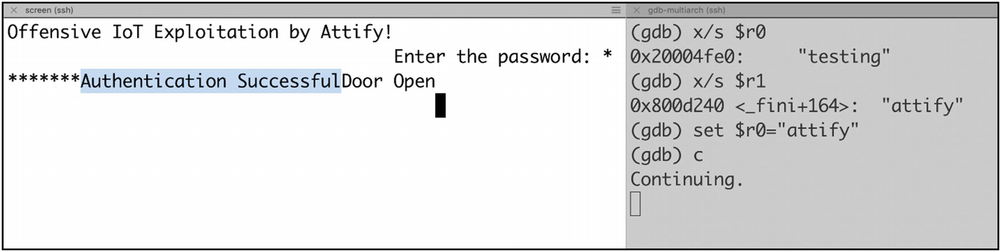
Authentication bypassed using JTAG debugging
That is how we can exploit a binary over JTAG and perform real-time debugging of the binary and modify one of the registers to make the authentication valid.
Conclusion
In this chapter, we had a look at one of the most interesting ways of exploiting embedded devices, which is via JTAG. However, the techniques and content covered in this chapter are intended to help you get started with JTAG debugging and I hope you will apply these skills to real-world devices to take it even further.
Also, once you have gained JTAG debugging access, it depends on how much further you want to go with it. This means that because you can debug binaries, you might find more vulnerabilities in the various binaries running on the device, which could help you compromise the device in further ways.