
In this chapter, we have a look at two of the other (apart from UART) most common serial protocols, namely I2C (pronounced I-2-C or I-square-C) and SPI, and see how they are useful for our security research and exploitation of IoT devices. Both SPI and I2C are useful bus protocols used for data communications between different components in an embedded device circuit. SPI and I2C have many similarities and a couple of differences in the way they function and how we interact with them.
We primarily use SPI and I2C exploitation techniques to dump contents (including firmware and other sensitive secrets) from a device’s flash chip, or write content (e.g., a malicious firmware image) to the flash chip, both of which are extremely useful techniques during a penetration test or while performing security research on an IoT device. However, because SPI and I2C are bus protocols, you will encounter them at many other places apart from just using them in Flash, such as Real Time Clocks (RTCs), LCDs, microcontrollers, analog-to-digital converters (ADCs), and so on. For this chapter, though, we focus on the underlying protocols and then look at how we could use these protocols to work with Flash and EEPROMs. We start with I2C and then move to SPI, understanding how we can interact with both and use them for our purposes.
I2C (Inter-Integrated Circuit)
Let’s start with a bit of background history on why I2C was created and how it evolved. I2C was developed in 1982, by Philips, to enable their chips to communicate and exchange data with other components. In the first version of I2C, the highest data transmission speed was 100 kbps with a 7-bit address, which then later improved to 400 kbps with a 10-bit address. At present, components using I2C can communicate with each other with a speed of up to 3.4 Mbps.
Looking at the technical aspects of I2C, it’s a multimaster protocol with only two wires required to enable data exchange—serial data (SDA) and serial clock (SCL). However, I2C is only half-duplex, which means it can only send or receive data at a given point of time.
Why Not SPI or UART
It might appear confusing at first: Why would someone use I2C instead of UART or SPI? Well, there are a couple of reasons.
The challenge with UART is the limitation of facilitating communication between only two devices at a given time. Additionally, as we have seen in the previous chapter, a UART packet structure includes a start and stop bit, which adds to the overall size of the data packet that is transferred, also affecting the speed of the entire process. Additionally, UART was originally intended to provide communication over large distances, interacting with external devices via cables. In contrast, I2C and SPI are meant for communicating with other peripherals located on the same circuit board.
SPI is another extremely popular protocol for data transfer between components. SPI has faster data transmission rates compared to I2C, but the only major downside that SPI has is the requirement of three pins for data transfer and one pin for Chip/Slave select, which increases the overall requirement of space while implementing the SPI protocol for data communication compared to I2C.
Serial Peripheral Interface
SPI is one of the other most popular communication protocols used in embedded devices. SPI is full-duplex (unlike I2C, which is half-duplex) and consists of three wires—SCK, MOSI, and MISO—and an additional chip select/slave select. In cases when there is no data to read, though, when there is a write happening, the slave should send dummy data to make the connection happen.
SPI was originally developed by Motorola to provide full-duplex synchronous serial communication between the master and slave devices. Unlike I2C, in SPI only one single master is controlling all the slaves and the master controls the clock for all the slaves. The overall implementation and standardization of SPI is pretty loosely defined and different manufacturers can modify the implementation in their own way, due to the lack of a strict standard. To understand the SPI communication for any given chip on the target device, the best way is to look up the data sheet and analyze how our target has implemented the SPI protocol for communication.
Understanding EEPROM
Both SPI and I2C are common protocols when it comes to talking about data storage via Electrically Erasable Programmable Read Only Memory (EEPROM). In this section, we look into EEPROM and understand the various pins in it, which will be useful while working with I2C and SPI.
Connections for Interacting with SPI EEPROM
Pin name | Function |
|---|---|
#CS | Chip select |
SCK | Serial data clock |
MISO | Serial data input |
MOSI | Serial data output |
GND | Ground |
VCC | Power supply |
#WP | Write protect |
#HOLD | Suspends serial input |
Chip select: Because both SPI and I2C (and other protocols) usually have multiple slaves, it is required to be able to select one slave among others for any given action. The chip select pin helps exactly in that—helping select an EEPROM when the #CS is low. When a device is not selected, there will be no communication happening between the master and the slave, and the serial data output pin remains in a high impedance state.
Clock: The clock or the SCK (or CLK) pin determines with what speed the data exchange and communication should take place. The master is the one that determines the clock speed that the slaves must adhere to. However, in the case of I2C, the slaves can modify and slow down the clock if the clock speed selected by the master is too fast for the slaves. This process is also known as clock stretching.
MISO/MOSI: MISO and MOSI, as you might have expected, stand for master-in-slave-out and master-out-slave-in, respectively. Depending on who is sending data and who is receiving, the pins are used. In case of I2C, because it’s half-duplex, it can only either read or write data at a given point in time. However, in the case of SPI, both read and write data happens at the same time. If there is no data to be sent (in read or write), dummy data is sent.
Write protect: As the name suggests, this pin allows normal read/write operations when it is high. When the #WP pin is active low, all write operations are inhibited.
HOLD: When a device is selected and a serial sequence is underway, #HOLD can be used to pause the serial communication with the master device without resetting the serial sequence. To resume the serial sequence, the #HOLD pin should be made high while the SCK pin is low.
Also, as we have discussed, I2C works on two lines, namely SDA and SCL. The SDA line is for the data exchange, whereas the clock line, SCL, is controlled by the master and determines the speed at which the data exchange takes place. The master also holds the address and memory location of all the various slave devices that are used during any communication.
In I2C, unlike SPI, there can be multiple masters interacting with various slaves. That configuration is called a multimaster mode. You might wonder what would happen if two masters wanted to take control over an I2C bus at the same time. The answer is that whichever master pulls the SDA to LOW (0) will gain control of the bus; that is, zero rushes to win.
Exploiting I2C Security
Now that we have a good understanding of the foundational concepts of I2C and how the data transfer happens, let’s jump into how we can exploit the devices using the I2C protocol. By exploiting I2C here, I mean reading or writing data of the device using an I2C EEPROM in a real-world device.
For this section, you can choose any device that has a flash chip working on the I2C communication protocol. For the purposes of demonstration, I’ll be taking an example of an unnamed smart glucometer, which has a feature of saving health records of the user offline on the device. For the purpose of hands-on lab exercises, you can get any device with EEPROM working on I2C communication protocol such a as GY-521 breakout board or even any I2C chips from https://www.digikey.in/en/ptm/m/microchip-technology/ic-serial-eeprom and use an EEPROM adapter to connect to it. The connections would remain the same as mentioned in the upcoming sections, no matter which I2C EEPROM device you choose to go with.
Data sheet of EEPROM
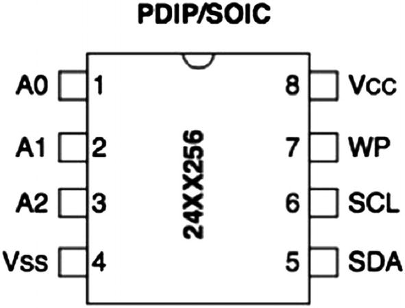
Pinouts from the data sheet of EEPROM
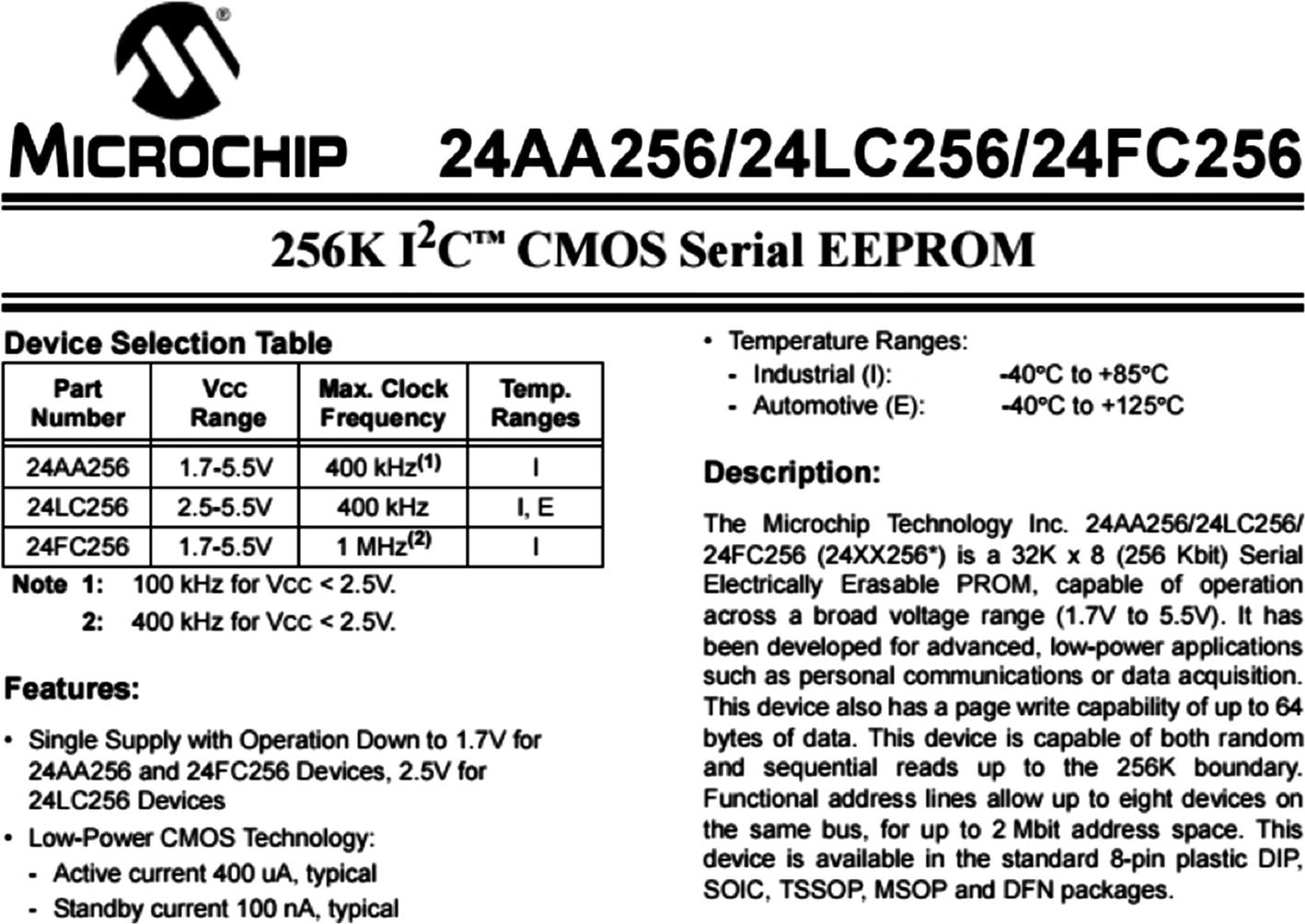
Pin Explanations for I2C EEPROM
Pin | Description |
|---|---|
A0 | User-configurable address bit |
A1 | User-configurable address bit |
A2 | User-configurable address bit |
VSS | Ground |
VCC | 1.7V to 5.5V (based on the model) |
WP | Write protect (active low) |
SCL | Serial clock |
SCK | Serial data |
Making Connections for I2C Exploitation with the Attify Badge
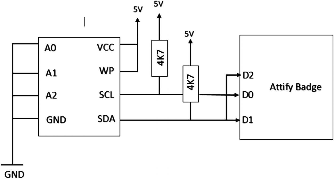
Attify Badge connections with EEPROM
A0, A1, A2, and GND are connected to GND.
Vcc and WP are connected to 5V, as write protect is active low.
D1 and D2 of Attify Badge are connected, which is the SDA line.
D0 is connected to the I2C SCL (Clock) line.
Once we have made all the connections, let’s look at the script that we are going to use to read and write data from I2C EEPROM.
Understanding the Code
To work with I2C, we will use the script i2ceeprom.py by Craig Heffner located at https://github.com/devttys0/libmpsse/blob/master/src/examples/i2ceeprom.py .
Before actually running the script, let’s try to understand how the script works. This will also be useful if you want to modify the script for your own requirements. You’ll also need to modify the script a bit while working with different I2C EEPROMs with different configurations and speeds.

EEPROM content is dumped
Similarly, we can also write data to the I2C chip.
Open the device.
Identify the I2C chip on the PCB.
Note the component number printed on the I2C chip.
Look online for the data sheet to determine the pinouts.
Make the required connections.
Use the i2ceeprom.py script to read or write data to the I2C EEPROM.
Digging Deep into SPI
Now that we understand I2C and EEPROM, let’s dig deeper into how SPI works and how to interact with target devices using the SPI communication protocol.
Serial clock (SCK).
Master-out-slave-in.
Master-in-slave–out.
Slave select (SS; active low, output from master) .
Out of these lines, the SCK, MISO, and MOSI pins are shared by slaves, whereas each SPI slave will have its own unique SS line. In SPI (unlike I2C) there can be only one master and multiple slaves. The master in SPI is the one in charge of the clock.
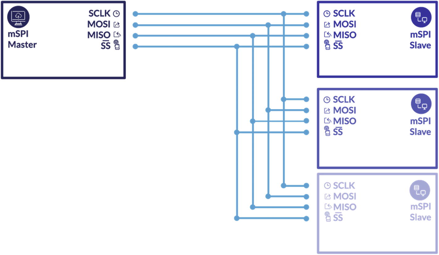
SPI master–slave configuration
The speed of SPI is not limited and that is why SPIs are typically faster than other protocols. Also, the fact that it is full-duplex makes it a better choice for device developers who want to utilize the speed.
How SPI Works
The master first configures the clock frequency according to the slave device’s clock frequency—typically up to a few MHz.
The fastest clock speed we can have in SPI is half the speed of the master clock. For instance, if the master runs at 32 MHz, the maximum serial clock rate can be up to 16 MHz.
To start communication, the master selects the slave device with a logic level 0 on the SS line. Remember that for every clock cycle, a full-duplex data transmission occurs.
The master initiates the communication by sending a bit on the MOSI line, which is read by the slave, whereas the slave sends a bit on the MISO line, which is read by the master. The most significant bit (MSB) is shifted out first and a new least significant bit (LSB) is shifted into the same register. Once the register bit has been shifted out and in, the master and slave have successfully exchanged the register value.
Reading and Writing from SPI EEPROM
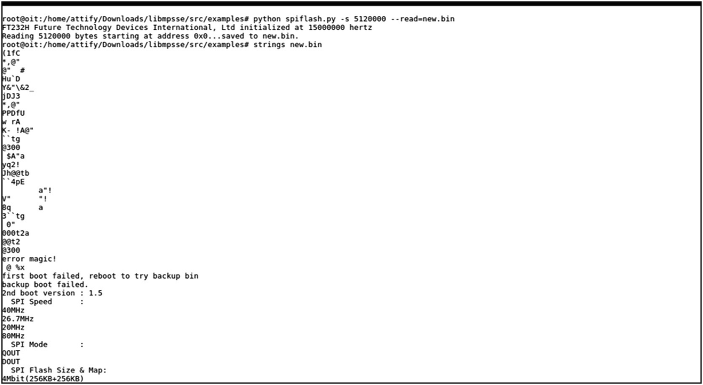
To read and write data from or to an SPI EEPROM, we use a utility called spiflash.py available to download from https://github.com/devttys0/libmpsse/ .
As you can see, we can set values such as specifying whether to read, write, or erase, as well as provide size to read and write, starting address to perform the operation, and custom clock frequency instead of the default 15 MHz. We also have an option of -v, which will verify if the data that has been written or read from the chip is the same as the original one.
Now that we are familiar with the script, we are ready to go ahead and try it on a target device. In my case, I have a Winbond SPI flash that I have removed from the PCB via desoldering. Once it is desoldered, we can then solder it to an EEPROM adapter (or reader). You could also directly read it while the chip is on the device by hooking miniprobes to the EEPROM or using a SOIC clip of a real-world IoT device without removing the chip from the device.

Windbond SPI EEPROM
Let’s go ahead and get started with making all the necessary connections for SPI. To do this, we need to first understand the pinouts of our target SPI flash chip, which in our case is W25Q80DVSNIG.
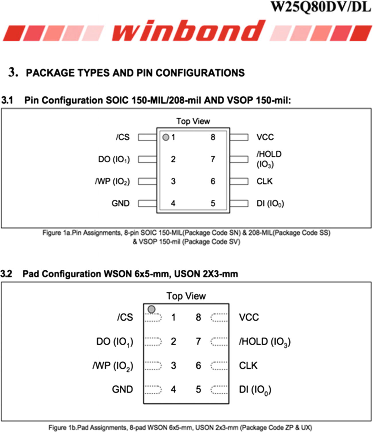
Flash chip pinouts
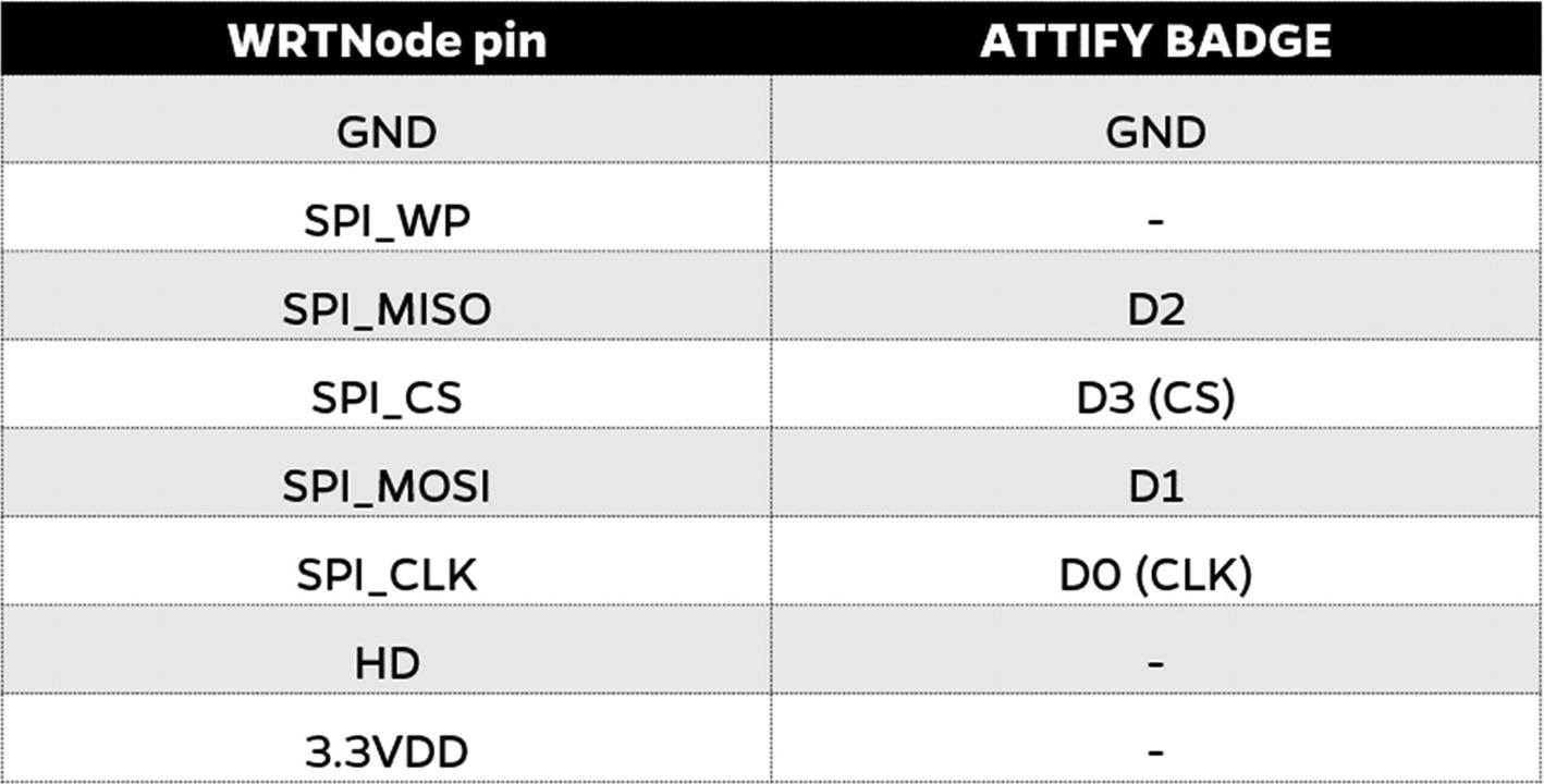
Connections for SPI Flash Read/Write Using Attify Badge
Pin on Attify Badge | Functionality during SPI communication |
|---|---|
D0 | SCK |
D1 | MISO |
D2 | MOSI |
D3 | CS |
Connect CLK to SCK (D0).
Connect MOSI/DO to MISO (D1).
Connect MISO/DI to MOSI (D2).
Connect CS to CS (D3).
Connect WP, HOLD, and Vcc to 3.3V.
Connect GND to GND.
One of the things that we need to note here is that the connections of MOSI and MISO will reverse if you are using another tool instead of Attify Badge (e.g., the Bus Pirate). This is because of the naming conventions of Attify Badge.
Dumping data from an EEPROM

Writing data to an EEPROM
This is extremely useful, as we can write a modified version of a device’s firmware if we are able to interact with the EEPROM flash chip over SPI.
Dumping Firmware Using SPI and Attify Badge
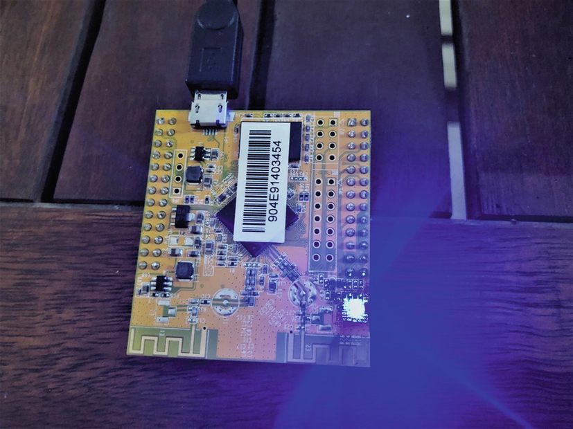
WRTNode device that uses SPI protocol for reading/writing to and from flash chip
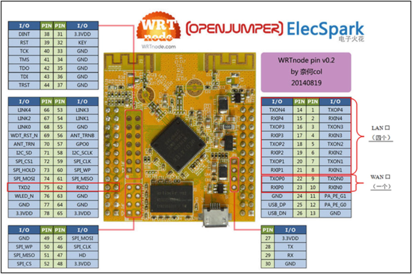
WRTNode pinouts: Note the SPI communication interface pinout at the bottom left
Now because we are already familiar with the SPI communication protocol and how to interact with devices using this protocol with Attify Badge, we can interact with WRTNode. In this case, if we read data from the flash chip, it will be the entire firmware, which we can then extract the file system from. Even though we cover firmware analysis and file system extraction in Chapter 7, I’ll show you briefly here the process of dumping firmware from a device using SPI.
Connection of WRTNode and Attify Badge for SPI firmware dumping
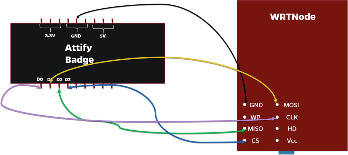
Connection of WRTNode and Attify Badge for SPI firmware dumping

Dumping firmware from the WRTNode using Attify Badge
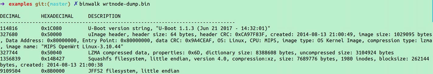
Extracting file system from the firmware
This is how we apply the SPI exploitation skill sets on real-world devices to dump the entire firmware from the device.
Conclusion
In this chapter, we covered several topics including EEPROM, I2C, and SPI. We also had a look at how we can read and write data from the EEPROM using both I2C and SPI communication protocols. This knowledge would be extremely useful for you when you are pentesting a real-world device and want to look at the firmware, which would be stored in the EEPROM, or any sensitive information.
You can also modify a firmware image dumped from the EEPROM chip and write it back and analyze the device’s behavior.
In the next chapter, we start looking at one of the other most popular concepts in embedded device hacking, JTAG.
Often, you’ll find real-world commercial devices storing content such as secret keys, firmware, binaries, and interesting data pieces in its EEPROM flash, which with the knowledge gained from this chapter, can be exploited.