
3 Fundamentals of Molecular Layer Deposition (MLD)
As described in Chapter 1, to realize high-performance photonic/electronic devices consisting of organic functional thin films, growth methods for polymer wires and molecular wires with designated (1) molecular sequences, (2) locations, and (3) orientations are essential. Molecular layer deposition (MLD) [1, 2, 3, 4, 5 and 6] is a method to grow polymer wires and molecular wires with designed molecular sequences, enabling precisely controlled growth of artificial polymer wires and molecular wires. MLD for growth of polymer wires utilizes chemical reactions between source molecules. MLD for growth of molecular wires, in which different kinds of molecules are aligned in designated sequences, utilizes electrostatic force between source molecules.
In the present chapter, the concept of MLD is reviewed, and the proof of concept is experimentally demonstrated. Selective wire growth for location and orientation control of polymer/molecular wires, which can be combined with MLD, is also described.
3.1 Concept of MLD
3.1.1 MLD UTILIZING CHEMICAL REACTIONS
The concept of MLD utilizing selective chemical reactions between source molecules [1] is shown in Figure 3.1 for a case in which four kinds of molecules are used: molecules A, B, C, and D. These molecules are prepared under the following guidelines.
A molecule has two or more reactive groups.
Reactive groups in a molecule cannot react with reactive groups in the same kind of molecules. For example, reactive groups in molecule A cannot react with reactive groups in molecule A.
Reactive groups in a molecule can react with reactive groups in other kinds of molecules. For example, reactive groups in molecule A can react with reactive groups in molecule B.
Thus, the same kinds of molecules cannot be connected, and different kinds of molecules can be connected through the reactions between groups. The molecular connections are achieved by chemical force. In the case shown in Figure 3.1, strong chemical reactions occur between molecules A–B, B–C, C–D, and D–A, and weak reactions between molecules A–A, B–B, C–C, D–D, A–C, and B–D.
In MLD, there are two typical growth configurations—one-sided growth and two-sided growth. For the one-sided growth, as shown in Figure 3.1(a), when molecule A is provided to a surface, a monomolecular layer of molecule A is formed. Once the surface is covered with molecule A, the deposition of the molecules is automatically terminated due to the small reactivity between the same kinds of groups, giving rise to thickness saturation. When molecules are switched from A to B, molecule B is connected to molecule A to induce a rapid thickness increase followed by saturation, exhibiting monomolecular step growth. This enables us to carry out sequential self-limiting reactions, like atomic layer deposition (ALD) [7,8], by switching molecules. When molecules are switched from B to C, molecule C is connected to molecule B. Similarly, when molecules are switched from C to D, molecule D is connected to molecule C. By repeating the switching with designated sequences, artificial polymer wires with a molecular sequence like ABCD … can be obtained.
For two-sided growth, as shown in Figure 3.1(b), molecule A is adsorbed on a surface. When molecule B is provided to the surface, molecules B is connected to both sides of molecule A. Once both sides of molecule A are covered with molecules B, the deposition of the molecules is automatically terminated due to the self-limiting effect, forming a BAB structure. By switching molecules from B to C, molecule C is connected to both sides of the BAB structure to form a CBABC structure. Similarly, by switching molecules from C to D, molecule D is connected to both sides of the CBABC structure to form a DCBABCD structure. By repeating the switching with designated sequences, artificial polymer wires with a molecular sequence like … DCBABCD … can be obtained with monomolecular step growth.
If a molecule with three reactive groups is used as shown in Figure 3.2(a), three-way branching polymer wires can be constructed. Similarly, more than four-way branching polymer wires can be constructed by using a molecule with more than four reactive groups. Bending of polymer wires is also possible by using a molecule with two reactive groups substituted in appropriate configurations.
An additional advantage of MLD is that it can deposit ultrathin conformal films on three-dimensional surfaces with arbitrary shapes, such as trenches, cylinders, pours/rough surfaces, and so on, as shown in Figure 3.2(b), in a manner similar to ALD.
3.1.2 MLD UTILIZING ELECTROSTATIC FORCE
The concept of MLD utilizing repulsive and attractive electrostatic force between source molecules [5,6] is shown in Figure 3.3 for one-sided growth. When four kinds of molecules are used, attractive force is generated in the combination of molecules A–B, B–C, C–D, and D–A, and repulsive force is generated in the combinations of molecules A–A, B–B, C–C, D–D, A–C, and B–D.
When molecule A is provided to a surface, a monomolecular layer of molecule A is formed. Once the surface is covered with molecule A, the deposition of the molecules is automatically terminated due to the repulsion between the same kinds of molecules, giving rise to thickness saturation. When molecules are switched from A to B, molecule B is connected to molecule A to induce a rapid thickness increase followed by saturation, exhibiting monomolecular step growth. When molecules are switched from B to C, molecule C is connected to molecule B. Similarly, when molecules are switched from C to D, molecule D is connected to molecule C. By repeating the switching with designated sequences, artificial molecular wires with a molecular sequence like ABCD … can be obtained. As in MLD for polymer wire growth, two-sided growth configurations might be possible.
FIGURE 3.1 Concept of MLD utilizing chemical reactions. (a) One-sided growth and (b) Both-sided growth. From T. Yoshimura, Trends in Thin Solid Films Research (ed. A. R. Jost), Ch. 5 “Self-Organized Growth of Polymer Wire Networks with Designed Molecular Sequences for Wavefunction-Controlled Nano Systems.” Nova Science Publishers, New York (2007).
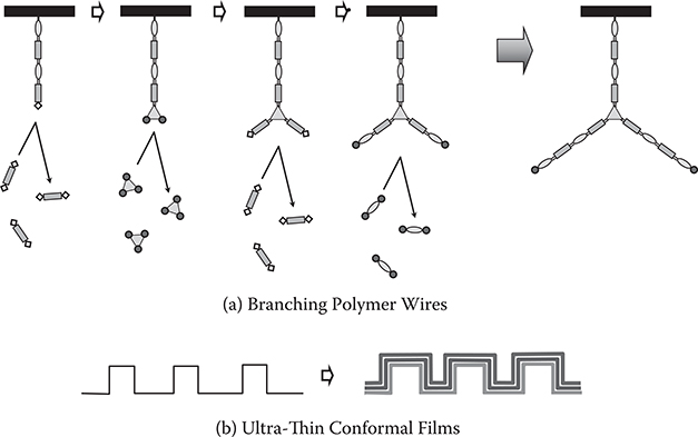
FIGURE 3.2 Growth of (a) branching polymer wires and (b) ultra-thin conformal films on three-dimensional surfaces by MLD.
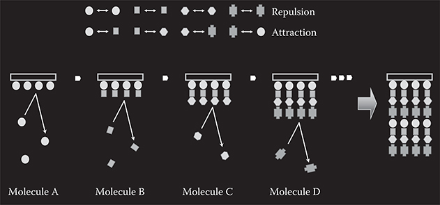
FIGURE 3.3 Concept of MLD utilizing electrostatic force.
3.1.3 MLD WITH MOLECULE GROUPS
Usually MLD is carried out by introducing one kind of molecule onto substrates at a molecular supplying step. In MLD with molecule groups, several kinds of molecules are introduced at the same molecular supplying step.
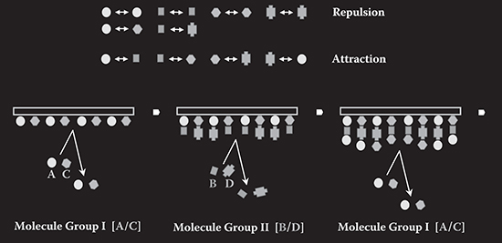
FIGURE 3.4 Concept of MLD with molecule groups.
In the example depicted in Figure 3.4, Molecule Group I containing molecules A and C and Molecule Group II containing molecules B and D are prepared. By providing molecules onto the substrate in the order of Molecule Group I, Molecule Group II, Molecule Group I, molecular wires of ABA, ABC, ADA, ADC, CBC, CBA, CDC, and CDA are formed in parallel.
In some cases, such feature that molecular wires or polymer wires with different molecular arrangements are grown simultaneously is useful, as described in Section 9.1.1.
3.2 MLD Equipment
In MLD, source molecules are supplied onto a substrate surface in gas phase or liquid phase. The former is the gas-phase MLD like K cell–type MLD and carrier gas–type MLD, and the latter is the liquid-phase MLD like fluidic circuit–type MLD.
3.2.1 GAS-PHASE MLD
3.2.1.1 K Cell–Type MLD
Figure 3.5 shows a schematic illustration and a photograph of the K cell–type MLD [1]. Molecular gases are provided onto a surface in vacuum from low-temperature K cells, in which source molecules are loaded. Molecular gas switching is performed by shutters. When the vapor pressure of the source molecules is high, molecular gases leak from the gap between the K cells and the shutters. In such cases, valves are used for the molecular gas switching.
3.2.1.2 Carrier Gas–Type MLD
Figure 3.6 shows a schematic illustration and a photograph of the carrier gas–type MLD [9,10], in which carrier gas is employed to introduce molecular gases in temperature-controlled molecular cells onto a substrate surface. Molecular gas switching is performed by valves. The molecules are combined through chemical reactions on the surface, while excess gases are removed with the carrier gas to a pump.
FIGURE 3.5 K cell-type MLD.
To ensure removal of remaining molecules and by-products generated by the chemical reactions used in the previous steps, gas purges with inert gases before the next molecular gas injection is effective.
The carrier gas-type MLD has the following advantages.
By-products generated by the chemical reactions are swept away from the surfaces by carrier gas flows.
The carrier gas prevents contaminations in the surrounding region from reaching the substrate surface.
Stable supply rates of molecular gases can be easily maintained.
Items 1 and 2 can keep the surface clean, which is especially important to carry out MLD. If by-products remain near the surface and molecules are adsorbed on them, polymer wires will grow randomly from the by-product sites. This will prevent polymer wires from growing with the designated orientations and locations. Furthermore, by-products may terminate polymer wire growth when their presence is near the wire edges. Contaminations such as remaining molecules used in the previous steps also prevent MLD from performing normal molecule-by-molecule growth. Therefore, the removal of contamination is essential in MLD of orientation-controlled long wires with designated locations.
FIGURE 3.6 Carrier gas-type MLD.
The carrier gas–type MLD does not always need to be carried out in high vacuum since, as described previously, the carrier gas flow isolates the substrate surface from outside to maintain desirable reactions between reactive groups of the molecules on the surface and reactive groups of the supplied molecules.
The advantages for the carrier gas–type MLD can similarly be found in the carrier gas–type organic chemical vapor deposition (CVD), where carrier gas is employed to introduce two or more kinds of molecular gases onto a substrate surface simultaneously. The molecules are combined through chemical reactions on the surface. Although the growth mechanism of the carrier gas–type organic CVD is similar to that of vacuum deposition polymerization, the former has the advantage that clean surfaces and stable gas flows are easily maintained during growth.
FIGURE 3.7 Fluidic circuit–type MLD.
3.2.2 LIQUID-PHASE MLD
3.2.2.1 Fluidic-Circuit Type MLD
Figure 3.7 shows a schematic illustration of the fluidic circuit–type MLD as an example of liquid-phase MLD. Source molecules are carried with solvent to be supplied on a surface. The molecules supplied to substrate surfaces are switched by valves. To ensure removal of remaining molecules, cleaning solvent injection during molecular switching is necessary. Fluidic processes using capillary circuits are effective to reduce the volume of solutions required for the MLD and solution switching duration. The liquid-phase MLD makes it easy to add catalysts for polymer wire or molecular wire growth.
It should be noted that liquid-phase MLD can be performed in human bodies for medical applications. In this case, for example, the human body corresponds to the chamber and the substrates correspond to cancer cells, and molecules are introduced from outside of the bodies by injection. By introducing different kinds of molecules into the bodies with designated sequences by injections, polymer wires or molecular wires will be grown on the cancer cells.
3.3 Proof of Concept of MLD
3.3.1 MLD UTILIZING CHEMICAL REACTIONS
MLD utilizing chemical reactions can be applied to a variety of polymers with covalent bonds arising from various kinds of reactive groups such as carbonyl-oxy-carbonyl groups, amino groups, −CHO groups, epoxy ring, −NCO groups, and so on. In the present section, in order to present proofs of concept of MLD for polymer wires, MLD of polyimide and polyazomethine (poly-AM) is shown using the K cell–type MLD.
FIGURE 3.8 Molecules and reactions for polyamic acid wire growth.
3.3.1.1 Polyimide
To demonstrate MLD, growth dynamics of polymer wires on a surface were investigated using molecule A and molecule B [1]. For the experiments, two sets of combinations of source molecules were considered. One is a set of A: pyromellitic dianhydride (PMDA) and B: 2,4-diaminonitrobenzene (DNB), and the other is a set of A: PMDA and B: 4,4’-diaminodiphenyl ether (DDE). The molecular structures and reactions are shown in Figure 3.8 [11,12]. The molecules are connected by reactions between the carbonyl-oxy-carbonyl group in molecule A and the amino group in molecule B to form alternately connected polymer wires. The reactions between carbonyl-oxy-carbonyl and carbonyl-oxy-carbonyl, and between amino and amino are weak, forming no bonds between molecules. From PMDA and DNB, polymer wires of polyamic acid [PMDA/DNB] are formed, and from PMDA and DDE, polymer wires of polyamic acid [PMDA/DDE]. By heating the polyamic acid in vacuum, polyimide is obtained.
Molecules A and B were evaporated separately from temperature-controlled K cells. The supplied molecules were selected by shutters on the K cells. The background pressure was 5 × 10⁻⁶ Pa and molecular gas pressures 1−5 × 10⁻³ Pa. The thickness of deposited films was measured using a quartz oscillator thickness monitor. The monitor head contacted the heated holder and was secured by an aluminum belt. The temperature was measured using a thermocouple on the holder. It is suspected that the actual temperature of the thickness monitor head was lower than that displayed. In this report, we used the displayed value as substrate temperature Ts for the sake of convenience.
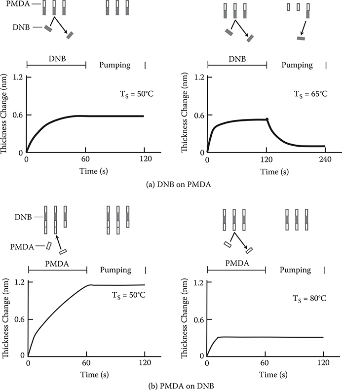
FIGURE 3.9 Thickness change versus shutter operations in MLD of polyamic acid [PMDA/DNB]. From T. Yoshimura, S. Tatsuura, and W. Sotoyama, “Polymer films formed with mono-layer growth steps by molecular layer deposition,” Appl. Phys. Lett. 59, 482–484 (1991).
Figure 3.9(a) shows the thickness change versus shutter operations for DNB growth on PMDA. Here, shutter A is for PMDA and shutter B for DNB. First, PMDA molecules are introduced on the surface by opening shutter A to form the PMDA layer. For duration td, both shutters A and B are closed. DNB molecules are then supplied onto the PMDA layer by opening shutter B. For Ts = 50°C, the film thickness rapidly increases and saturates in 40 s after shutter B opens. Thickness is maintained after shutter B closes. The change in thickness is 0.6 nm, close to the molecular size of DNB. The time dependence of the change in thickness is not affected by td from 5 to 60 s, which excludes the possibility that the thickness changes due to PMDA molecules remaining just after shutter A is closed.
These results suggest that a monomolecular step growth of DNB is achieved on the PMDA as follows. The binding energy between PMDA and DNB, that is, between carbonyl-oxy-carbonyl and amino, is larger than that between DNB and DNB (amino and amino). So the DNB molecules can be connected to the PMDA molecules. Once the surface is covered with DNB molecules, additional DNB molecules cannot be connected onto the surface to terminate the growth automatically.
When DNB is supplied to the PMDA layer at Ts = 65°C, a similar thickness increase and saturation as at Ts = 50°C is observed. When both shutters are closed after DNB layer growth, however, the film thickness decreases to the initial value. This means that DNB molecules re-evaporate from the surface before strong bonds between DNB molecules and PMDA molecules are formed. When we consider that the average time for DNB to remain at the surface corresponds to the time constant of the thickness decay, the average time is about 30 s at Ts = 65°C.
Figure 3.9(b) shows the thickness change versus shutter operations for PMDA growth on DNB. When PMDA is supplied to a DNB layer at Ts = 50°C, an initial rapid increase in thickness is observed. Thereafter, the thickness continues to gradually increase and does not saturate. This indicates that PMDA molecules condense on the surface to form a multimolecular layer. When the substrate temperature is raised to 80°C, the thickness saturates, indicating that PMDA condensation is avoided at this temperature and mono molecular step growth of PMDA on DNB is achieved.
As described, the optimum temperature for monomolecular step growth differs for DNB on PMDA and for PMDA on DNB. This may be due to the difference in vapor pressure between PMDA and DNB. To fabricate polymer wires by repeatedly stacking with monomolecular steps, the substrate temperature must be elevated synchronously with molecule switching.
Figure 3.10 shows an example of MLD using PMDA for molecule A and DDE for molecule B. Mono molecular step growth is observed at the same temperature of Ts = 80°C for both DDE on PMDA and PMDA on DDE. Therefore, MLD can be done without elevating the substrate temperature. This might be attributed to the fact that vapor pressures of PMDA and DDE is not largely different. A 10-nm-thick polymer film of polyamic acid was deposited by MLD with 15 steps of alternate molecule supply. By annealing in vacuum, the polyamic acid is converted into polyimide, as shown in Figure 3.11.
It should be noted that recently the gas-phase MLD utilizing chemical reactions was drastically advanced. Putkonen et al. succeeded in growing thick polyimide films of several hundred nm by MLD with over 500 steps [13]. Salmi et al. reported inorganic-organic nanolaminates consisting of polyimide and Ta2O5 that are applicable to photonic gratings [14]. George et al. clarified surface reactions for MLD and developed new approaches in MLD [15], including the three-step ABC process using ring-opening and heterobifunctional reactants. The process suppresses double reactions, enabling long-wire growth. Liang and Weimer achieved the conformal coating of ultrathin aluminum alkoxide (alucone) polymer films on silica and titania nanoparticles as well as fabrication of porous films having voids with designed sizes [16]. Loscutoff et al. applied rigid and thermally stable nano-scale oligourea films, in which hydrogen bonds exist between neighboring oligomer wires, grown by MLD to copper diffusion barriers in nanoelectronics [17].
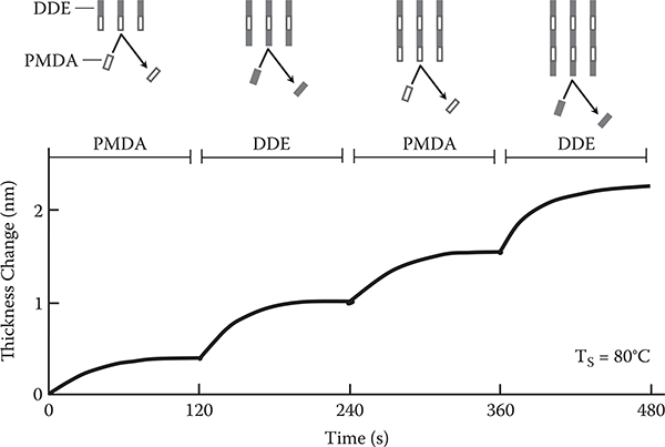
FIGURE 3.10 Thickness change versus shutter operations in MLD of polyamic acid [PMDA/DDE]. From T. Yoshimura, S. Tatsuura, and W. Sotoyama, “Polymer films formed with monolayer growth steps by molecular layer deposition,” Appl. Phys. Lett. 59, 482–484 (1991).
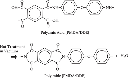
FIGURE 3.11 A conversion reaction from polyamic acid to polyimide.
3.3.1.2 Conjugated Polymers
MLD can be applied to molecule-by-molecule growth of conjugated polymers. As shown in Figure 3.12, by using terephthalaldehyde (TPA) for molecule A and p-phenylenediamine (PPDA) for molecule B, conjugated polymers of poly-AM [TPA/PPDA] are grown. TPA and PPDA react through –CHO in TPA and –NH2 in PPDA to form –C=N–inducing π-conjugated systems [12]. When oxalic acid (OA) and oxalic dihydrazide (ODH) react, conjugated polymers of poly-oxadiazole (OXD) are synthesized with the assistance of heating in a vacuum [18].
We demonstrated MLD of poly-AM using TPA and PPDA [19]. Figure 3.13 shows the results. When PPDA is provided on TPA with a molecular gas pressure of 1−8 x 10⁻² Pa, steplike growth of ~0.7 nm that is close to the molecule size is observed at a substrate temperature TS = 25°C. After removing PPDA from the vacuum chamber, by providing TPA on PPDA existing at the top surface with a molecular gas pressure of 10−1 Pa or more, steplike growth is observed again. These results indicate that mono-molecular step growth with self-limiting is achieved by MLD. It is also observed that the thickness is proportional to the molecular gas switching count, just like ALD. The molecule-by-molecule growth characteristics of MLD enable us to obtain desired properties of polymers with controlled π-electron wavefunction shapes.
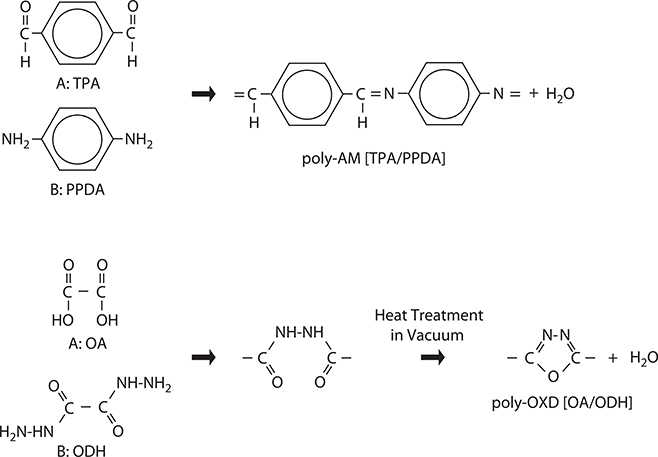
FIGURE 3.12 Molecules and reactions for polymer wire growth of conjugated polymers: poly-AM and poly-OXD.
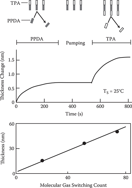
FIGURE 3.13 (a) Thickness change versus shutter operations, and (b) thickness versus molecular gas switching count characteristics in MLD of poly-AM [TPA/PPDA]. From T. Yoshimura, S. Tatsuura, W. Sotoyama, A. Matsuura, and T. Hayano, “Quantum wire and dot formation by chemical vapor deposition and molecular layer deposition of one-dimensional conjugated polymer,” Appl. Phys. Lett. 60, 268–270 (1992).
3.3.2 MLD UTILIZING ELECTROSTATIC FORCE
MLD can be applied to molecular wires, in which different kinds of molecules are aligned by the electrostatic force with designated sequences. In this subsection, as a proof of concept for MLD utilizing electrostatic force, formation of stacked structures of p-type and n-type dye molecules on ZnO surfaces is presented. In addition, MLD in molecular crystals of charge-transfer complexes is briefly described.
3.3.2.1 Stacked Structures of p-Type and n-Type Dye Molecules on ZnO Surfaces
In the 1970s, K. Kiyota et al. were able to self-assemble p-type dye molecules and n-type dye molecules on semiconductor surfaces [20]. The self-assembling of the dye molecules itself provides the proof of concept for the MLD utilizing electrostatic force.
To analyze the molecular assembling structures on semiconductor surfaces, surface potential measurements were used [21]. Samples used for the measurement were prepared as follows. For the semiconductor, a ZnO powder layer was spread on a glass substrate with a SnO2 electrode. For the first dye molecule adsorption, 0.01 mL of an alcohol solution of the first dye molecule with a concentration of 1.6 mol/L was dropped on the ZnO layer (3 cm2 area). For the second dye molecule adsorption, an alcohol solution of the second dye molecule was similarly dropped on the surface, where the first dye molecules were already adsorbed. Structures of various p-type and n-type dye molecules are illustrated in Figure 3.14. In the present experiment, rose bengal (RB) and bromphenol blue (BPB) were used for the p-type dye molecules, and malachite green (MG) and crystal violet (CV) for the n-type dye molecules.
Figure 3.15 shows the surface potential of a ZnO layer and ZnO layers adsorbing the first dye molecules. The surface potential of the ZnO layer without dye molecule adsorption is about −200 mV. When p-type dye molecules are adsorbed on the ZnO layer, the surface potential becomes more negative than the ZnO layer without dye molecule adsorption. Conversely, when n-type dye molecules are adsorbed, the surface potential becomes less negative.
This result can be explained as follows. In ZnO, zinc atoms in interstitial positions donate their electrons to oxygen adsorbed on the ZnO surface to generate electric dipoles, causing a negative surface potential for the ZnO layer. When p-type dye molecules are adsorbed on the ZnO surface, electrons in the ZnO layer are transferred to the dye molecules to generate additional electric dipoles with the same direction as that of the dipoles arising from the oxygen, enhancing the total electric dipole moment at the ZnO surface. In the case of an n-type dye molecule, conversely, the electrons in the dye molecules are transferred to the ZnO layer to generate electric dipoles with opposite direction, which suppresses the total electric dipole moment at the ZnO surface. Kokado et al. found that conductivity of the ZnO layer was raised by adsorption of n-type dye molecules and reduced by adsorption of p-type dye molecules, and they attributed the phenomenon to the transfer of electrons between the dye molecules and the ZnO [22]. The results of the surface potential measurements are consistent with their findings.
Figure 3.16 shows the surface potential of ZnO layers adsorbing the first dye molecules and the second dye molecules successively. Here, MG→RB indicates that the first dye molecule is MG and the second dye molecule is RB. As can be seen in the figure, variation of the surface potential arising from the adsorption of two dye molecules mainly depends on the second dye molecule. This indicates that the twodye-molecule-stacked structure is definitely constructed and the surface potential is determined by differences in Fermi levels between the second dye molecules (the top molecules) and the ZnO layer.
The surface potential of the samples, in which p-type and n-type dye molecules are coadsorbed on the ZnO layer simultaneously, is also shown in Figure 3.16. RB + MG indicates the coadsorption of RB and MG. For the coadsorption of p-type and n-type dye molecules, 0.01 mL of an alcohol solution containing both p-type dye molecules and n-type dye molecules at equal concentrations of 1.6 mol/L is dropped on the ZnO layer. The surface potential of the ZnO layer coadsorbing the p-type and n-type dye molecules is very similar to that of the ZnO layer adsorbing p-type dye molecules as the first dye molecule and n-type dye molecules as the second dye molecule. This suggests that p-type dye molecules and n-type dye molecules are self-assembled to form a stacked structure of a ZnO/p-type dye molecule/n-type dye molecule.
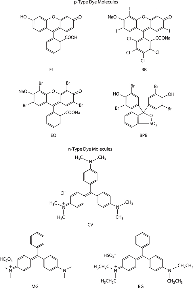
FIGURE 3.14 Structures of p-type and n-type dye molecules. Fluorescein: FL, Rose bengal: RB, Eosine: EO, Bromphenol blue: BPB, Crystal violet: CV, Malachite green: MG, and Brilliant green: BG.
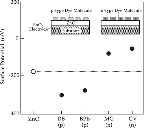
FIGURE 3.15 Surface potential of a ZnO layer and ZnO layers adsorbing dye molecules. From T. Yoshimura, K. Kiyota, H. Ueda, and M. Tanaka, “Contact potential difference of ZnO layer adsorbing p-type dye and n-type dye,” Jpn. J. Appl. Phys. 18, 2315–2316 (1979).
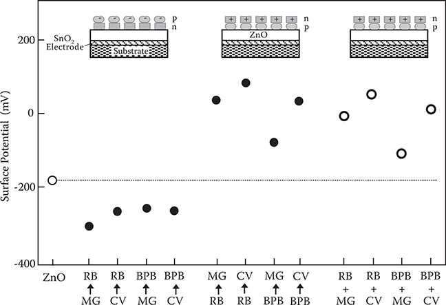
FIGURE 3.16 Surface potential of ZnO layers adsorbing the first dye molecules and the second dye molecules successively, and surface potential of ZnO layer coadsorbing p-type dye molecules and n-type dye molecules simultaneously. From T. Yoshimura, K. Kiyota, H. Ueda, and M. Tanaka, “Contact potential difference of ZnO layer adsorbing p-type dye and n-type dye,” Jpn. J. Appl. Phys. 18, 2315–2316 (1979).
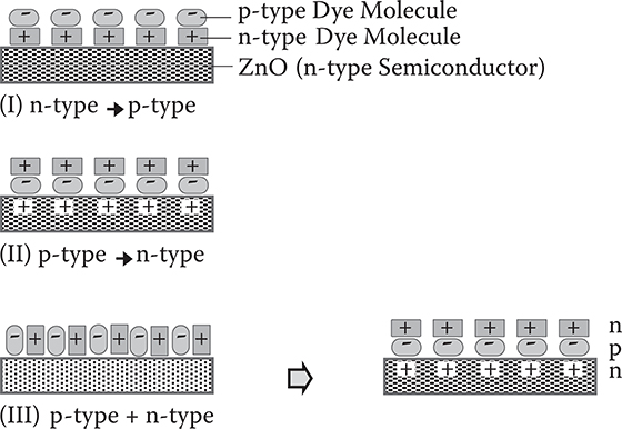
FIGURE 3.17 Assembled structures of p-type and n-type dye molecules stacked on ZnO surfaces.
In Figure 3.17, assembled structures of p-type and n-type dye molecules stacked on ZnO surfaces are summarized. When p-type dye molecules and n-type dye molecules are coadsorbed simultaneously, dye molecules are self-assembled in the order of a p-type dye molecule and an n-type dye molecule on an n-type ZnO to form npn structures. The self-assembling arises from electron transfers from ZnO to p-type dye molecules and from n-type dye molecules to p-type dye molecules, resulting in a strong connection due to electrostatic force between ZnO and p-type dye molecules, and n-type dye molecules and p-type dye molecules. The self-assembling effect strongly suggests the viability of MLD utilizing electrostatic force.
Actual experimental demonstration of MLD utilizing electrostatic force is presented in Chapter 9, Section 9.1.3, where, multidye sensitization is described.
The concept of the self-assembled structures of the p-type and n-type molecules provides the base for the self-assembled monolayers (SAM) developed in 1980s. As Figure 3.18 shows, in the case of SAM, two different molecules are combined into one molecule to achieve the self-assembling. The SAM is currently applied to surface treatment for various kinds of organic thin-film devices.
3.3.2.2 Molecular Crystals
It is known that tetrathiafulvalene (TTF) and tetracyanoquinodimethane (TCNQ) combine through charge transfers between them to form molecular crystals of charge transfer complexes. From this property, it is expected that MLD utilizing electrostatic force might be accomplished using these molecules. Figure 3.19 shows MLD of TTF on TCNQ. As in the PMDA/DNB, PMDA/DDE, and TPA/PPDA systems, monomolecular adsorption occurs. TTF re-evaporates when shutter A is closed, however, suggesting that the connecting force between TTF and TCNQ is not sufficient. Since the time constant for thickness decay increases with decreasing substrate temperature, by optimizing the substrate temperature, we might be able to apply MLD to charge transfer complexes.
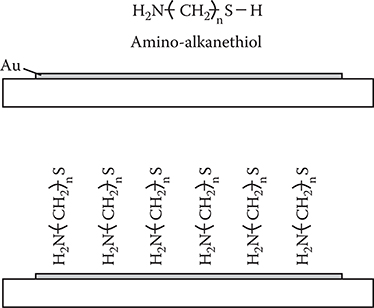
FIGURE 3.18 Self-assembled monolayer.
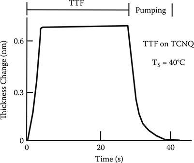
FIGURE 3.19 MLD of TTF on TCNQ.
3.4 MLD with Controlled Growth Orientations and Locations
In order to construct thin-film organic photonic/electronic devices and molecular nano systems consisting of self-organized polymer/molecular wire networks, three-dimensional growth with location and orientation control by MLD is required. To do this we proposed wire growth from seed cores.
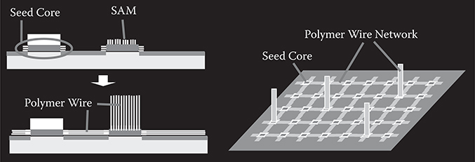
FIGURE 3.20 The concept of the seed-core-assisted MLD for three-dimensional growth. From T. Yoshimura, Y. Suzuki, N. Shimoda, T. Kofudo, K. Okada, Y. Arai, and K. Asama, “Three-dimensional chip-scale optical interconnects and switches with self-organized wiring based on device-embedded waveguide films and molecular nanotechnologies,” Proc. SPIE 6126, 612609-1-15 (2006).
The concept of the seed-core-assisted MLD is shown in Figure 3.20 [3,4,23]. On the top surfaces and/or sidewalls of the seed cores, the SAM is formed selectively. The seed cores are used for controlling polymer wire growth locations and orientations. For vertical growth, the SAM is put on the top of the seed cores, while for horizontal growth it is put on the sidewalls. The regions, where polymer wires should not grow are covered with, for example, SiO2 films. By distributing the seed cores with designated patterns, polymer wires are expected to grow with designated configurations, constructing polymer wire networks.
It should be noted that the three-dimensional growth orientation control technique using seed cores can be applied not only to MLD, but also to other growth methods such as vacuum deposition polymerization and organic CVD.
In this section, using the carrier gas–type MLD, we demonstrate vertical growth of poly-AM wires from seed cores with amino-alkanethiol SAM on Au films [9,10].
3.4.1 GROWTH CONTROL BY SEED CORES
3.4.1.1 MLD from SAM
Wires of poly-AM, a conjugated polymer, were grown from seed cores by MLD using source molecules of TPA and PPDA. The carrier gas was nitrogen (N2), and the molecular cell temperature was 50°C. Figure 3.21 shows the schematic illustration for the process of molecule-by-molecule growth of poly-AM wires by the carrier gas–type MLD. In step 0, in order to anchor seed core molecules to a substrate surface, a SAM of amino-alkanethiol (11-amino-1-undecanethiol) was formed on patterned Au films deposited on a glass substrate. The SAM formation was carried out by putting the substrate in an ethanol solution of 11-amino-1-undecanethiol, hydrochloride, and then rinsing and drying it. In step 1, TPA molecules were provided onto the surface by opening the valve for TPA. The surface was exposed to TPA molecular gas for 5 min, to connect TPA to the SAM. In step 2, after removing TPA molecular gas by closing the valve for TPA and pumping for 5 min, the valve for PPDA was opened. The surface was exposed to PPDA molecular gas for 5 min, to connect PPDA to TPA. TPA and PPDA were alternately introduced onto the surface by switching the valves, reaching step m. In the present case, TPA and PPDA were respectively provided onto the surface 10 times, that is, m = 20. Thus, poly-AM grown on a substrate with SAM was obtained. For the purpose of comparison, poly-AM grown on a substrate without SAM was also prepared by the same procedure described above.
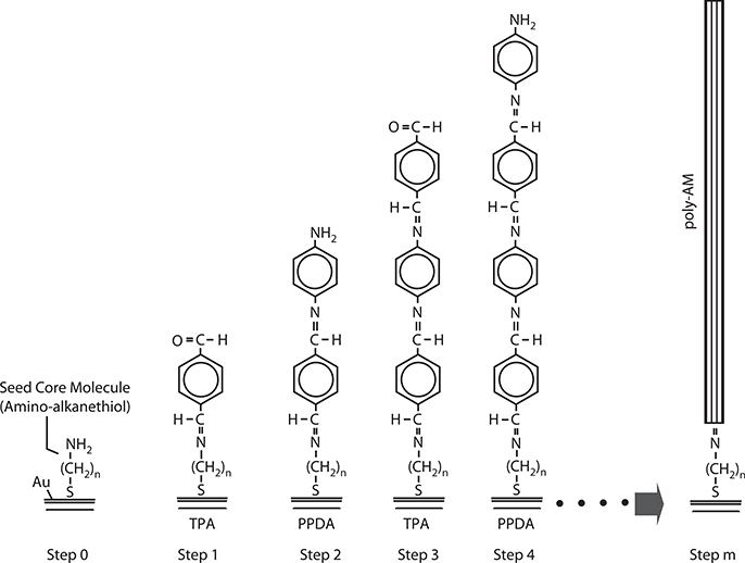
FIGURE 3.21 Process of molecule-by-molecule growth of poly-AM wires. From T. Yoshimura, S. Ito, T. Nakayama, and K. Matsumoto, “Orientation-controlled molecule-by-molecule polymer wire growth by the carrier-gas-type organic chemical vapor deposition and the molecular layer deposition,” Appl. Phys. Lett. 91, 033103-1-3 (2007).
Figure 3.22 shows the Fourier transform infrared reflection absorption spectroscopy (FTIR-RAS) spectra of TPA-adsorbed surfaces (step 1). The absorption peaks attributed to TPA in wavenumber regions around 820 cm−1 and 780 cm−1 are larger for the sample that was prepared using a surface with SAM (denoted by “SAM surface”) than those for the sample that was prepared using a surface without SAM (denoted by “non-SAM surface”). When the sample temperature was raised to 45°C, the peak height in the non-SAM surface decreased while that in the SAM surface did not decrease. These results indicate that more TPA molecules exist on the surface with stronger adsorption strengths in the case of the SAM surface than in the case of the non-SAM surface, suggesting that TPA–SAM connections are constructed in the SAM surface.
Figure 3.23 shows the FTIR-RAS spectra of poly-AM grown by the carrier gas–type MLD (step m = 20). It can be seen that both the SAM surface and the non-SAM surface exhibit absorption peaks in wavenumber regions around 1200 to 1300 cm−1 and 850 cm−1. The former and the latter peaks are attributed respectively to the vibration of in-plane direction (denoted by “in-plane”) and the vibration of surface-normal direction (denoted by “surface-normal”) in benzene rings. The absorbance ratio of in-plane to surface-normal (I In-Plane/I Surface-Normal) is larger by a factor of about 2 in the SAM surface than in the non-SAM surface. This suggests that polymer wires tend to grow along nearly vertical directions in the SAM surface as the model shown in Figure 3.21 while wires tend to grow along nearly horizontal directions in the non-SAM surface.
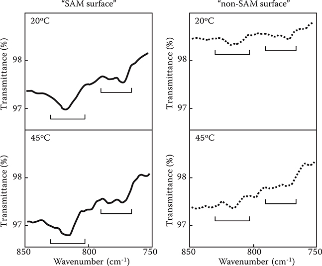
FIGURE 3.22 FTIR-RAS spectra of TPA-adsorbed surfaces (step 1). From T. Yoshimura, S. Ito, T. Nakayama, and K. Matsumoto, “Orientation-controlled molecule-by-molecule polymer wire growth by the carrier-gas-type organic chemical vapor deposition and the molecular layer deposition,” Appl. Phys. Lett. 91, 033103-1-3 (2007).
3.4.1.2 Organic CVD from SAM
In order to confirm the poly-AM wire growth direction described above, we carried out polymer wire growth by the carrier gas–type organic CVD on SAM surfaces and non-SAM surfaces [9]. Molecular cell temperature T Molecular Cell and carrier gas flow rate R Flow were 50°C and 4 NL/min, respectively. The results are shown in Figure 3.24. In the case of the non-SAM surface, film thickness increases at the initial stage, followed by saturation. On the other hand, film thickness increases linearly with growth time in the case of the SAM surface. These results can be explained in terms of reaction site densities on surfaces.
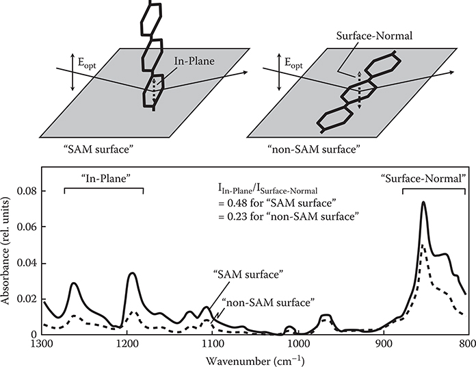
FIGURE 3.23 FTIR-RAS spectra of poly-AM grown by the carrier gas–type MLD (step m = 20). From T. Yoshimura, S. Ito, T. Nakayama, and K. Matsumoto, “Orientation-controlled molecule-by-molecule polymer wire growth by the carrier-gas-type organic chemical vapor deposition and the molecular layer deposition,” Appl. Phys. Lett. 91, 033103-1-3 (2007).
As shown in the model illustrated in Figure 3.25, TPA and PPDA molecules adsorb on an Au-coated substrate horizontally in the case of the non-SAM surface, resulting in horizontal poly-AM wire growth. Since the –CHO group and the –NH2 group are hydrophilic, TPA and PPDA molecules are preferably adsorbed to –CHO and –NH2 groups at the edge of poly-AM wires while they do not adsorb to the other parts of poly-AM wires that are hydrophobic. The density of hydrophilic sites that exist at the edge of the poly-AM wires decreases as poly-AM wires grow, and then the growth rate of poly-AM films decreases, resulting in the film thickness saturation. Here, although CH=N, which appears at each unit of body parts of the wires, has H-bond acceptor characteristics, the polarity of CH=N is smaller compared to that of NH2 and CHO. So, the model shown in Figure 3.25 is still viable as the 0th approximation.
As Figure 3.26 shows, the contact angle of a water droplet is 44.6° on a SiO2 surface. The angle increases after poly-AM is grown on the surface. The contact angles of water droplets on the surfaces increase with growth time followed by saturation. This indicates that the surface changes from hydrophilic states to hydrophobic states, confirming the reduction of the hydrophilic site density at the surface.
In the case of the SAM surface, on the other hand, TPA and PPDA molecules adsorb on the substrate vertically. So, poly-AM wires grow vertically, keeping the density of the hydrophilic sites constant. Therefore, poly-AM film thickness does not exhibit saturation.
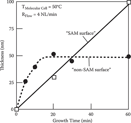
FIGURE 3.24 Growth time dependence of the poly-AM film thickness in the carrier gas–type organic CVD. From T. Yoshimura, S. Ito, T. Nakayama, and K. Matsumoto, “Orientation-controlled molecule-by-molecule polymer wire growth by the carrier-gas-type organic chemical vapor deposition and the molecular layer deposition,” Appl. Phys. Lett. 91, 033103-1-3 (2007).
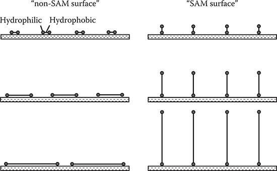
FIGURE 3.25 Model for poly-AM growth by the carrier gas–type organic CVD. From T. Yoshimura, S. Ito, T. Nakayama, and K. Matsumoto, “Orientation-controlled molecule-by-molecule polymer wire growth by the carrier-gas-type organic chemical vapor deposition and the molecular layer deposition,” Appl. Phys. Lett. 91, 033103-1-3 (2007).
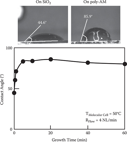
FIGURE 3.26 Growth time dependence of the contact angle of water droplets on the surfaces. From T. Yoshimura, S. Ito, T. Nakayama, and K. Matsumoto, “Orientation-controlled molecule-by-molecule polymer wire growth by the carrier-gas-type organic chemical vapor deposition and the molecular layer deposition,” Appl. Phys. Lett. 91, 033103-1-3 (2007).
It is clearly indicated from these results that nearly vertical molecule-by-molecule growth of conjugated polymer wires can be achieved on substrates with SAM by the carrier gas–type MLD. This enables three-dimensional self-aligned growth by using seed cores, which is ultrasmall, for example, nm-scale Au blocks with SAM on the top surfaces and/or sidewalls. The seed cores are distributed with designed configurations on a substrate. Polymer wires are expected to grow vertically from the top surfaces and horizontally from the sidewalls to form polymer wire networks by providing molecular gases to the substrate.
It should be noted that, in the vacuum deposition polymerization, film thickness of poly-AM increases with growth time without saturation for the non-SAM surface. The reason why the growth saturation that occurs in the carrier gas–type organic CVD does not occur in vacuum deposition polymerization can be explained in terms of the previously described advantage (1) of the carrier gas–type organic CVD. During growth of poly-AM, H2O molecules are generated as by-products. In the case of vacuum deposition polymerization, some of the generated H2O molecules may weakly adsorb on the surface. Then, TPA and PPDA molecules can adsorb to the H2O molecules to initiate poly-AM growth from the adsorbed molecules. In other words, H2O molecules act as growth cores. Therefore, growth saturation does not occur. In the case of the carrier gas–type organic CVD, the generated H2O molecules on the surface are blown away by carrier gas molecules to prevent the growth initiation.
3.4.2 MONOMOLECULAR STEP POLYMER WIRE GROWTH FROM SEED CORES
Since required polymer/molecular wire lengths range from ~1 nm to several hundred nm depending on the application, it is important to clarify the polymer wire lengths that can be grown with perfect monomolecular steps by MLD. Using the carrier gas–type MLD, we investigated precise processes of monomolecular step growth of poly-AM wires from seed core molecules of amino-alkanethiol SAMs on Au film [10].
The MLD process is the same as that shown in Figure 3.21. A simulation based on the molecular orbital method (Fujitsu WinMOPACK) reveals that a poly-AM wire grows from the seed core molecule with a slight helix waving, as Figure 3.27 shows.
In the present experiment, the maximum step count was 18. The carrier gas–type MLD was performed in the following conditions: substrate temperature, 25°C; molecular cell temperatures, 25°C and 50°C for TPA and PPDA, respectively; blowing duration of molecular gases onto the surface, 1 min or 5 min; pumping duration for removing residual molecular gases, 5 min; and carrier gas flow rate, 4 NL/min.
In Figure 3.28, FTIR-RAS spectra of poly-AM wires grown by the carrier gas–type MLD with a molecular gas blowing duration of 5 min are shown for step 6. As described in Section 3.4.1, the absorbance ratio of IIn-Plane/ISurface-Normal is larger in the SAM surface than in the non-SAM surface, indicating that poly-AM wires tend to grow in upward directions in the SAM surface, while the wires tend to grow in horizontal directions in the non-SAM surface. It can be seen from Figure 3.29 that absorption spectra for a blowing duration of 1 min are almost the same as those for a blowing duration of 5 min, suggesting that a molecular gas blowing duration of 1 min is enough to complete the self-limiting monomolecular growth.
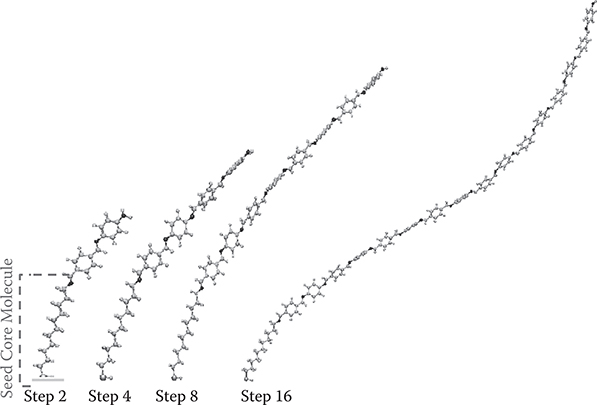
FIGURE 3.27 Simulation of poly-AM wire growth by the molecular orbital method.
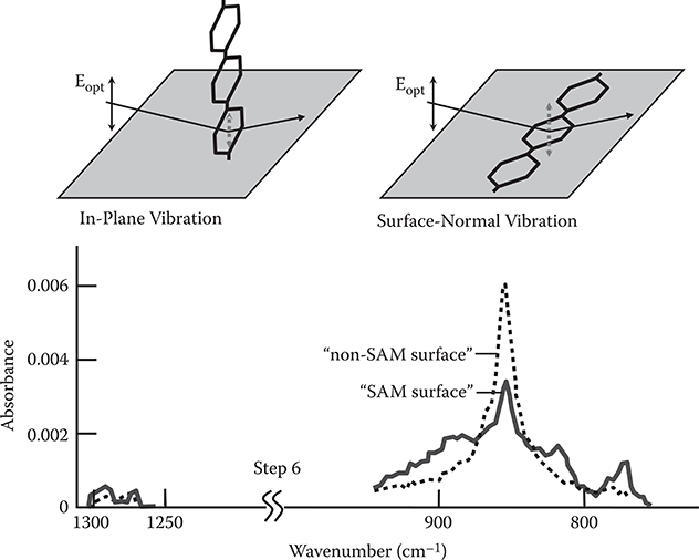
FIGURE 3.28 FTIR-RAS spectra of poly-AM wires grown by the carrier gas–type MLD with a molecular gas blowing duration of 5 min. From T. Yoshimura and Y. Kudo, “Monomolecular-step polymer wire growth from seed core molecules by the carrier-gas type molecular layer deposition (MLD),” Appl. Phys. Express 2, 015502-1-3 (2009).
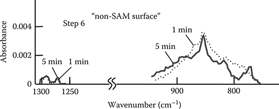
FIGURE 3.29 FTIR-RAS spectra of poly-AM wires grown by the carrier gas–type MLD with a molecular gas blowing duration of 1 min. From T. Yoshimura and Y. Kudo, “Monomolecular-step polymer wire growth from seed core molecules by the carrier-gas type molecular layer deposition (MLD),” Appl. Phys. Express 2, 015502-1-3 (2009).
FIGURE 3.30 Step count dependence of peak absorbance in the region around 850 cm−1 for poly-AM wires of SAM surface. From T. Yoshimura and Y. Kudo, “Monomolecular-step polymer wire growth from seed core molecules by the carrier-gas type molecular layer deposition (MLD),” Appl. Phys. Express 2, 015502-1-3 (2009).
Figure 3.30 shows the step count dependence of peak absorbance in the region around 850 cm−1 for poly-AM wires of the SAM surface. Until step 12, the absorbance linearly increases with step count. This indicates that perfect monomolecular step growth is achieved in a step count range from 1 to 12, which approximately corresponds to wire lengths of 0.5 to ~6 nm. In step 18, however, the absorbance deviates from the linear relationship, implying that the MLD process causes growth imperfection in long wires.
Although the reason for the deviation of the absorbance from the linear relationship is not clear at present, one possible reason is double reactions at the top surface during growth, as suggested by George [24]. The double reactions, in which two reactive groups of a molecule provided on the surface make chemical bonds with top reactive groups of two polymer wires simultaneously, may remove the active sites at the surface to reduce the MLD growth rate. Another possible reason is tangling of poly-AM wires, as indicated by Liskola [25]. The tangling that might be caused by the helix-shaped growth characteristics of poly-AM wires shown in Figure 3.27 may make the wire growth direction disordered.
In Figure 3.31, step count dependence of the absorbance ratio IIn-Plane/ISurface-Normal in poly-AM wires is shown. Until step 12, the absorbance ratio is larger in the SAM surface than in the non-SAM surface by a factor of 2~3. The result clearly indicates that, from step 1 to step 12, poly-AM wires tend to grow in upward directions in the SAM surface, while in the non-SAM surface, the wires tend to grow in horizontal directions. In step 18, the absorbance ratio in the SAM surface decreases, getting close to the absorbance ratio in the non-SAM surface. This result suggests that the growth direction of the poly-AM wires of the SAM surface is tilted. Possible reasons for the tilt might be the previously described double reactions and tangling.
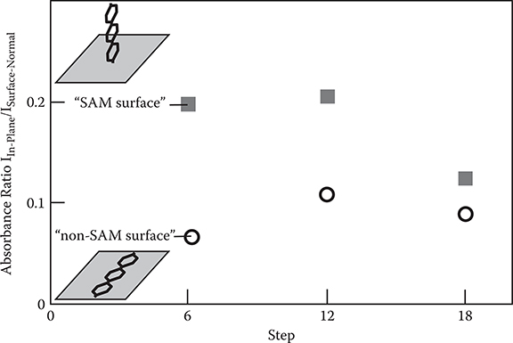
FIGURE 3.31 Step count dependence of absorbance ratio IIn-Plane/ISurface-Normal in poly-AM wires.
In order to achieve perfect monomolecular step upward growth from seed core molecules beyond the current limitation (~ step 12), precise optimization of the substrate temperature will be necessary. Iijima and Takahashi reported that 4,4’diamino-diphenyl ether molecules adsorb on a surface vertically at a substrate temperature of 40°C while they adsorb horizontally at 10°C [26]. If TPA and PPDA molecules have the same tendency, namely, they adsorb on the surface vertically at high substrate temperature, it is expected that the double reactions can be suppressed by raising the substrate temperature because the probability that the source molecules react with two active sites at the surface simultaneously is reduced when the source molecules stand vertically. Gas flow rates, which are one of the important parameters in MLD, should also be optimized.
3.5 High-Rate MLD
In conventional carrier gas–type MLD equipment, gas injection into a chamber and gas removal from the chamber are necessary for molecular gas switching, resulting in an increase in processing time. For example, in our conventional MLD equipment, it takes about 5 min for the gas injection and removal. In order to reduce the process time and increase the growth rate, the domain-isolated MLD was proposed [27].
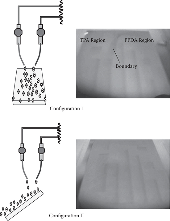
FIGURE 3.32 Influences of molecular gas flow on polymer film growth patterns in the carrier gas–type CVD. From K. Matsumoto and T. Yoshimura, “Electro-optic waveguides with conjugated polymer films fabricated by the carrier-gas-type organic CVD for chip-scale optical interconnects,” Proc. SPIE 6899, 98990E-1-9 (2008).
3.5.1 INFLUENCES OF MOLECULAR GAS FLOW ON POLYMER FILM GROWTH
It was found that carrier gas prevents outside gases from penetrating into the region in which the carrier gas flows. Figure 3.32 shows influences of molecular gas flow on polymer film growth patterns in the carrier gas–type CVD [28]. Two kinds of molecular gas flow configurations, I and II, were examined. In configuration I, where the substrate is tilted by 45° and TPA gas flow is parallel to PPDA gas flow, poly-AM grows only near the boundary between the TPA region and the PPDA region. The polymer is not deposited under the nozzles where only one kind of gas, that is, TPA or PPDA, exists. This indicates that source molecules cannot penetrate into the other regions, namely, the carrier gas blocks penetration of molecules from outside. Conversely, in configuration II, where TPA gas flow overlaps PPDA gas flow, poly-AM was formed in wide regions since the joining position of the two kinds of the molecular gases is spread over the substrate surface.
These results indicate a possibility that a plurality of molecular domains can coexist closely when the gas flow condition is adjusted.
3.5.2 DOMAIN-ISOLATED MLD
As described in Section 3.5.1, carrier gas blocks molecular penetration from outside when the gas flow configuration is appropriately adjusted. The unique characteristics enable us to develop the domain-isolated MLD, which enables high-rate MLD.
The rotation type domain-isolated MLD using two kinds of source molecules is schematically illustrated in Figure 3.33 (a). A nozzle for molecule A (denoted by A) and a nozzle for molecule B (denoted by B) are set on a substrate holder. Between the two nozzles, a nozzle for purge gas (denoted by P) is located. Substrates are put on the holder. By blowing gas containing molecules A, gas containing molecules B, and purge gas onto the substrates from these nozzles, a molecule A domain, a molecule B domain, and a purge gas curtain (PGC) are generated. the PGC prevents molecules in the two domains from mixing, and isolate the molecule A domain and the molecule B domain. By rotating the substrate holder, each substrate passes through the two domains alternately to achieve molecule-by-molecule growth of polymer wires by MLD.
Figure 3.33(b) is for the case using four kinds of source molecules. Nozzles for molecule A, molecule B, molecule C (denoted by C), and molecule D (denoted by D) are set around the center of the substrate holder. Between the four nozzles, nozzles for purge gas are located. By blowing gas containing molecule A, gas containing molecule B, gas containing molecule C, gas containing molecule D, and purge gas onto the substrates from these nozzles, a molecule A domain, a molecule B domain, a molecule C domain, a molecule D domain, and PGCs are generated. By rotating the substrate holder, each substrate passes through the four domains sequentially to achieve MLD.
Figure 3.34 shows train-type domain-isolated MLD using four kinds of source molecules. Nozzles for molecules A, B, C, and D are set in parallel to generate molecule A domains, molecule B domains, molecule C domains, and molecule D domains. Between these domains, PGCs are inserted. By moving substrates on a conveyor, each substrate sequentially passes through the domains to achieve MLD. When the gas blowing is switched by opening and closing the nozzle valves, arbitrary sequences of molecules are available. It is possible to bring the substrates back to the starting point to repeat MLD, which saves the number of required nozzles.
In order to examine the blocking ability of PGCs against molecular mixing, TPA/N2 gas and PPDA/N2 gas were simultaneously introduced onto a glass substrate in rotation-type MLD shown in Figure 3.33(a) without rotation. With increasing flow rates of N2 for the PGC from 2.0 NL/min to 8.0 NL/min, light absorption due to poly-AM films deposited by TPA/PPDA mixing was drastically suppressed, indicating that the PGC has enough blocking ability to isolate the molecular domains.
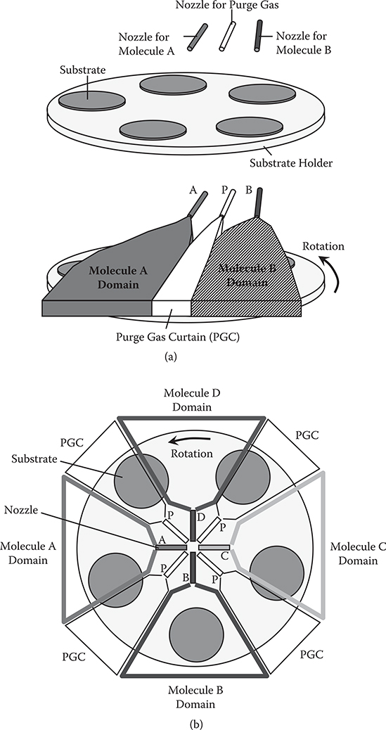
FIGURE 3.33 Domain-isolated MLD (Rotation Type). (a) For two kinds of source molecules and (b) for four kinds of source molecules.
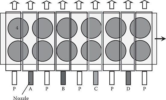
FIGURE 3.34 Domain-isolated MLD (Train Type).
Using a PGC with 8.0 NL/min, domain-isolated MLD of poly-AM with rotation counts of 9 and 20 (step counts of 18 and 40) were attempted. The rotation speed of the spin stage was 0.25 rpm. As can be seen in Figure 3.35(a), the absorption peak of poly-AM is about 2 times larger for a step count of 40 than for a step count of 18, suggesting that the thickness of poly-AM films is approximately proportional to the step counts. The time to complete the 40-step growth is about 80 min, while it is about 200 min in the conventional MLD equipment. Therefore, the growth rate increases by 2.5 times in the domain-isolated MLD, as compared with the conventional MLD.
The domain-isolated MLD using three kinds of source molecules, TPA, PPDA, and ODH, were also attempted. Figure 3.35(b) shows absorption spectra of films grown with step counts of 27 and 40. The growth time was fixed at 60 min for both cases, implying that the rotation speed is 1.5 times higher for a step count of 40 than for a step count of 27. It is found that the absorption peak height of the film, that is, the film thickness, increases by 1.3 times when the step count increases from 27 to 40. The film thickness ratio of 1.3 is fairly close to the step count ratio of 40/27 = 1.5, suggesting the feasibility of the domain-isolated MLD for three kinds of source molecules.
3.6 Selective Wire Growth
As described in Section 3.4, by using seed cores, precisely controlled three-dimensional growth of polymer wires and molecular wires is possible with designated locations and orientations by MLD. MLD enables similar controlled polymer/molecular wire growth with the assistance of selective wire growth. In Figure 3.36, the selective wire growth methods with MLD are summarized.
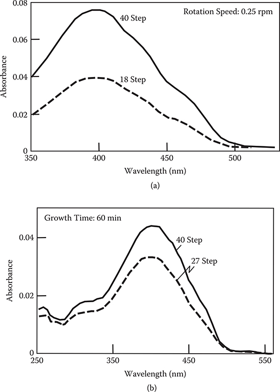
FIGURE 3.35 Absorption spectra of poly-AM grown by domain-isolated MLD (a) using TPA and PPDA with steps 18 and 40, and (b) using TPA, PPDA, and ODH with steps 27 and 40.
In the present section, the selective wire growth methods, such as selective growth and selectively-aligned growth, which utilize surface treatment of substrates and electric fields, are presented.
3.6.1 SELECTIVE GROWTH ON SURFACES WITH PATTERNED TREATMENT
The concept of selective growth of polymers using molecules A and B is shown in Figure 3.37. Molecules A and B are connected by chemical reactions to grow polymer wires. Surface treatment is applied to a substrate surface with designed patterns. In the example shown in Figure 3.37, the adsorption strength of molecules to the surface is stronger in the surface-treated region than in the untreated region.
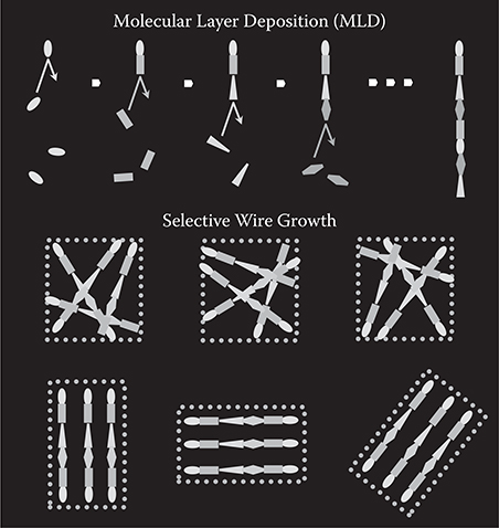
FIGURE 3.36 Selective wire growth methods. From T. Yoshimura, Trends in Thin Solid Films Research (ed. A. R. Jost) Ch. 5 “Self-Organized Growth of Polymer Wire Networks with Designed Molecular Sequences for Wavefunction-Controlled Nano Systems.” Nova Science Publishers, New York (2007).
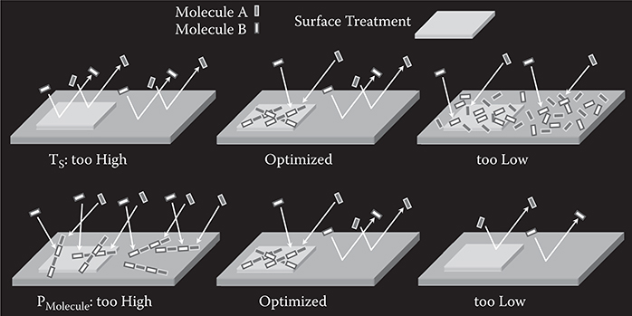
FIGURE 3.37 Selective growth. From T. Yoshimura, Trends in Thin Solid Films Research (ed. A. R. Jost) Ch. 5 “Self-Organized Growth of Polymer Wire Networks with Designed Molecular Sequences for Wavefunction-Controlled Nano Systems.” Nova Science Publishers, New York (2007).
In order to realize selective growth, optimization of substrate temperature TS and molecular gas pressure PMolecule is required. When TS is too high, the average time τS for molecules to remain at the surface becomes short, resulting in re-evaporation of molecules in all the surface regions before being combined with other molecules. When TS is too low, the molecules are aggregated all over the surface. At optimized TS, in the untreated region, molecules re-evaporate. In the treated region, τS becomes longer than in the untreated region due to stronger adsorption strength, enhancing collisions between molecules A and B. Then, molecules A and B can be combined to make new molecules with larger molecular weight, preventing the molecule from re-evaporation, and consequently, polymer wires grow. Thus, selective growth can be realized.
When PMolecule is too high, molecules are combined in all the surface regions, resulting in polymer wire growth in both the treated and untreated regions. When PMolecule is too low, molecules re-evaporate before collisions happen with other molecules. At optimized PMolecule, molecules re-evaporate in the untreated region while polymer wires grow in the surface-treated region, where τS is long enough to induce collisions between molecules A and B, enabling selective growth.
A process example of selective growth is shown in Figure 3.38. First, a hydro-phobic treatment is applied to a substrate surface. Then, a hydrophilic treatment is applied with a designed pattern on the surface, forming a hydrophilic/hydrophobic pattern. Finally, two kinds of reactive molecules are introduced onto the surface to grow a polymer thin film using chemical reactions between the molecules. When the hydrophilic surface is more favorable for molecule adsorption than the hydrophobic surface, reactions between the molecules occur only on the hydrophilic region, resulting in selective growth of a polymer thin film.
An experimental demonstration of selective growth was performed for poly-AM [TPA/PPDA] using patterned hydrophobic/hydrophilic surface treatment of glass substrates [29]. First, a hydrophobic treatment was applied to a glass substrate surface as follows. Hexamethyldisilazane (HMDS) was coated on the surface. After 1 h, the substrate was put into dichloromethane to remove excess HMDS from the surface to obtain a hydrophobic surface on the glass substrate. Next, a SiO thin film, 100 nm thick, was deposited with a designed pattern on the surface using vacuum evaporation. Since SiO is hydrophilic, a hydrophilic/hydrophobic pattern was formed on the surface. Finally, poly-AM wires were grown on the surface by introducing TPA and PPDA into a vacuum chamber for 150 min with a gas pressure around 0.1 Pa at TS = 25°C. Since the hydrophilic SiO surface is more favorable for TPA and PPDA molecule adsorption than the hydrophobic HMDS surface, reactions between the molecules are expected to occur only on the hydrophilic region, resulting in selective growth of poly-AM wires.
Figure 3.39 shows the result of poly-AM growth on the substrate with a hydrophilic/hydrophobic pattern. It is found from Figure 3.39(a) that a yellow rectangle (a dark rectangle in the monochromatic photograph) exists. The rectangular part corresponds to the region where the SiO thin film was deposited. The yellow color arises from 11-nm-thick poly-AM thin film that was confirmed by absorption spectra described later. In the surrounding region, where HMDS exists, the substrate exhibits no color, indicating little sign of poly-AM thin film growth. These results demonstrate that a poly-AM thin film selectively grows on the SiO region. The enlarged photograph in Figure 3.39(b) reveals that the boundary between the SiO region and the HMDS region has a sharp contrast, suggesting the potentiality of a high-resolution patterning.
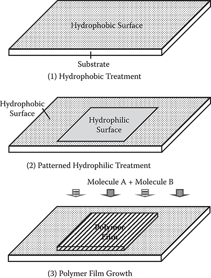
FIGURE 3.38 Process example of selective growth. From T. Yoshimura, N. Terasawa, H. Kazama, Y. Naito, Y. Suzuki, and K. Asama, “Selective growth of conjugated polymer thin films by the vapor deposition polymerization,” Thin Solid Films 497, 182–184 (2006).
Figure 3.40 shows absorption spectra of the SiO region and the HMDS region. An absorption band of poly-AM with a peak at ~410 nm appears for the SiO region while there is no absorption for the HMDS region. Therefore, the result confirms that poly-AM thin film is selectively grown on the SiO region, in other words, on the hydrophilic region.
The same selective growth of poly-AM can be realized by using triphenyldiamine (TPD) instead of HMDS as shown in Figure 3.41 [28]. When poly-AM film was grown by the carrier gas–type organic CVD on a glass substrate with patterned TPD thin films deposited by vacuum evaporation through a metal mask, poly-AM did not grow on TPD, on which PPDA and TPA molecules weakly adsorb since TPD is hydrophobic. Poly-AM selectively grew on the hydrophilic glass surface, on which PPDA and TPA molecules strongly adsorb.
As future challenges, selective growth of poly-AM on nano-scale patterns is interesting for photonic crystals and three-dimensional nano-scale optical circuits in optoelectronic large-scale integrated circuits (LSIs).
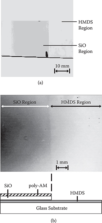
FIGURE 3.39 (a) Observation of selective growth for poly-AM, and (b) magnified photograph and schematic diagram near the boundary between the hydrophilic and the hydrophobic regions. From T. Yoshimura, N. Terasawa, H. Kazama, Y. Naito, Y. Suzuki, and K. Asama, “Selective growth of conjugated polymer thin films by the vapor deposition polymerization,” Thin Solid Films 497, 182–184 (2006).
3.6.2 SELECTIVELY-ALIGNED GROWTH ON ATOMICSCALE ANISOTROPIC STRUCTURES
In polymer functional devices like those described in Section 3.8, it is important to control polymer wire alignment. Selectively-aligned polymer wire growth techniques will provide a wide range of device structures. For example, if polymer wires are aligned selectively within a stripe with a width of submicron or micron scale, a channel optical waveguide can be constructed without etching because such selective alignment induces a refractive index difference between the stripe and surrounding regions. The polymer wire alignment is favorable for enhancing second-order or third-order optical nonlinearities of the optical waveguides. Carrier mobility in polymer thin-film transistors (TFTs) might also be increased by the alignment.
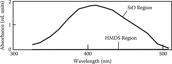
FIGURE 3.40 Absorption spectra of the SiO region and the HMDS region. From T. Yoshimura, N. Terasawa, H. Kazama, Y. Naito, Y. Suzuki, and K. Asama, “Selective growth of conjugated polymer thin films by the vapor deposition polymerization,” Thin Solid Films 497, 182–184 (2006).
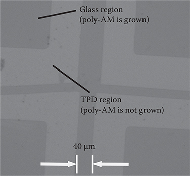
FIGURE 3.41 Selective growth of poly-AM using patterned TPD thin films. From K. Matsumoto and T. Yoshimura, “Electro-optic waveguides with conjugated polymer films fabricated by the carrier-gas-type organic cvd for chip-scale optical interconnects,” Proc. SPIE 6899, 98990E-1-9 (2008).
Kanetake et al. reported that aligned polydiacetylene film is grown by vacuum evaporation on rubbing polydiacetylene films [30]. Patel et al. showed that epitaxial growth induces selective alignment of spin-coated polydiacetylene films by patterning the rubbing polymer underlayer [31]. To develop an all-dry process, we attempted the selectively-aligned growth of poly-AM and polyimide wires on surfaces with anisotropic structures [32].
3.6.2.1 Concept
The concept of polymer wire alignment process by selectively-aligned growth utilizing patterned surface treatment with anisotropic structures is illustrated in Figure 3.42. First, an obliquely-evaporated dielectric film is deposited with designed patterns on a substrate, which is tilted along the y-axis by θ°. Here, θ is a tilting angle of the substrate surface normal direction from the evaporant beam direction. The dielectric film has ultra-fine anisotropic structures along the y-axis. Next, molecules A and B are introduced onto the surface to grow polymer wires. Wires grown on the obliquely-evaporated dielectric film are oriented in a direction parallel (or perpendicular) to the y-axis, while wires grown directly on the substrate surface are oriented in random directions. Thus, selectively-aligned growth is achieved.
The driving force for the polymer wire alignment might be interaction between the anisotropic structures of the dielectric film and molecules. The molecules tend to be placed on the dielectric film in a configuration at potential energy minimum. It should be noted that any surfaces having anisotropic potential energy distributions can be used for selectively-aligned growth instead of the obliquely-evaporated dielectric films.
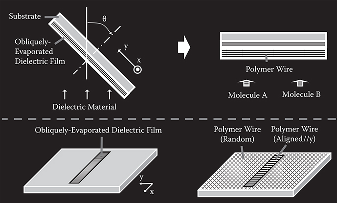
FIGURE 3.42 The polymer wire alignment process by selectively-aligned growth utilizing patterned surface treatment with anisotropic structures. From T. Yoshimura, Trends in Thin Solid Films Research (ed. A. R. Jost) Ch. 5 “Self-Organized Growth of Polymer Wire Networks with Designed Molecular Sequences for Wavefunction-Controlled Nano Systems.” Nova Science Publishers, New York (2007).
3.6.2.2 Growth
To demonstrate the proof of concept of selectively-aligned growth, poly-AM was grown on an obliquely-evaporated SiO2 film. In Figure 3.43, a schematic illustration of a cross-section of poly-AM wires grown on the obliquely-evaporated SiO2 film by selectively-aligned growth is shown. First, a SiO2 underlayer was deposited by the oblique evaporation on a quartz substrate at 10−3 Pa. The substrate was tilted by θ° along the y-axis. Film thickness ranged from 50 to 200 nm. Next, poly-AM films of 160 to 500 nm were deposited by introducing TPA and PPDA onto the surface. The molecular gases were introduced into a vacuum chamber from K cells heated at 100–130°C. The gas pressures were 1 to 8 × 10⁻¹ Pa, controlled by the cell temperatures. The substrate temperature was about 25°C. The obtained film was insoluble in methanol and acetone, confirming polymer formation.
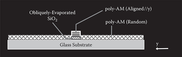
FIGURE 3.43 Schematic illustration of a cross-section of poly-AM wires grown on obliquely evaporated SiO2 film. From T. Yoshimura, Trends in Thin Solid Films Research (ed. A. R. Jost) Ch. 5 “Self-Organized Growth of Polymer Wire Networks with Designed Molecular Sequences for Wavefunction-Controlled Nano Systems.” Nova Science Publishers, New York (2007).
3.6.2.3 Optical Characterization for Selective Alignment of Polymer Wires
Figure 3.44 shows absorption spectra of the poly-AM for light polarization parallel and perpendicular to the y-axis. For θ = 0°, that is, a sample with an under-layer normally evaporated, the film shows no dichroism. For θ = 45°, on the other hand, absorption for EOpt//y is about ten times larger than for EOpt ⊥ y. The conjugated polymer has a large absorption for light polarization in the polymer wire direction. Therefore, the result indicates that the polymer wire is aligned along the y-axis in the poly-AM film on the SiO2 underlayer deposited by the oblique evaporation with tilting along the y-axis.
By using previously described phenomenon, selective alignment of the poly-AM wires was attempted for a 10-µm-wide stripe pattern of SiO2 via the following process (Figure 3.45(a)).
A photo-resist pattern window was formed on a quartz substrate for the 10-µm-wide stripe.
An 80-nm-thick SiO2 film was deposited on it by oblique evaporation with θ = 45° or θ = 0°. The substrate tilting direction, that is, the y-axis, was either perpendicular or parallel to the stripe.
The photo-resist was removed by the lift-off process, forming the 10-µm-wide SiO2 stripe.
A 160-nm polymer film was deposited over the entire substrate by vacuum deposition polymerization using TPA and PPDA.
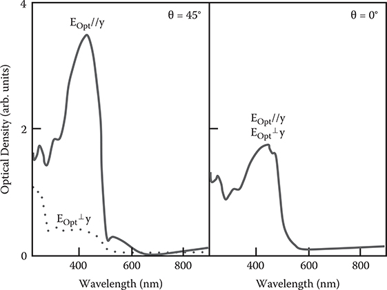
FIGURE 3.44 Absorption spectra of the poly-AM grown by selectively aligned growth with θ = 45° and 0° for light polarization parallel and perpendicular to the y-axis. From T. Yoshimura, K. Motoyoshi, S. Tatsuura, W. Sotoyama, A. Matsuura, and T. Hayano, “Selectively aligned polymer film growth on obliquely-evaporated SiO2 pattern by chemical vapor deposition,” Jpn. J. Appl. Phys. 31, L980–L982 (1992).
Figure 3.45(b) shows microscopic observation of the poly-AM with polarized light. In the case where θ = 45°, the obliquely-evaporated SiO2 region is darker than the surrounding region for light polarization parallel to the y-axis (EOpt//y), while the obliquely-evaporated SiO2 region is brighter than the surrounding region for light polarization perpendicular to the y-axis (EOpt⊥y). The results indicate that the wires on the obliquely-evaporated SiO2 are aligned along the y-axis, and wires on the glass substrate surface are randomly oriented as shown in Figure 3.43. In the case where θ = 0°, on the other hand, contrast between the SiO2 region and the surrounding region does not depend on light polarization, indicating that the poly-AM wires are random over the entire surface. These results confirm that selective alignment of polymer wires is realized by SiO2 underlayers deposited by oblique evaporation. Selective alignment was also observed in thick poly-AM films with thicknesses of 500 nm or more. By increasing θ from 0° to 60°, the degree of alignment was increased.
When, as shown in Figure 3.46(a), a 100-nm-thick SiO2 underlayer was obliquely evaporated by tilting the substrate along the y-axis on a SiO2 layer obliquely evaporated by tilting the substrate along the x-axis, the contrast between the stripe region and the surrounding region was completely inverted with rotating polarization from E//x to E//y (Figure 3.46(b)). This indicates that the wire direction in the stripe region is at right angles to that in the surrounding region. That is, the wires in the stripe region are aligned along the y-axis, and the wires in the surround region are aligned along the x-axis, as illustrated in Figure 3.46. This result means that the polymer wire directions are determined only by the SiO2 layer coming in contact with the polymer wires. Therefore, it is suggested that the polymer wire directions can freely be controlled with designated patterns on a substrate by stacking SiO2 underlayers obliquely evaporated with different tilting directions.
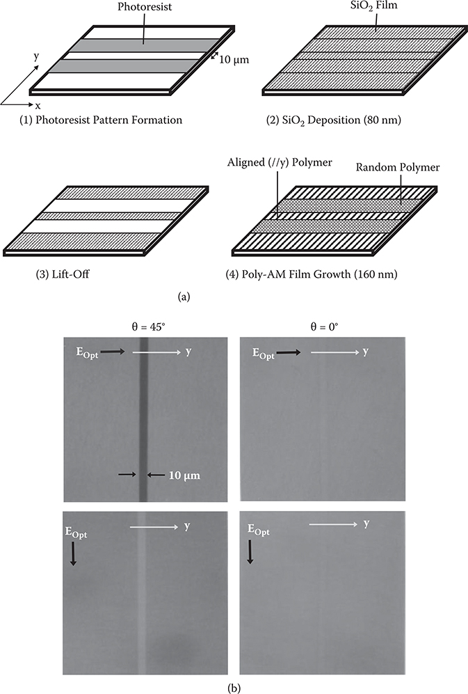
FIGURE 3.45 (a) Process for selective alignment of poly-AM wires, and (b) microscopic image observation of the poly-AM with polarized light. From T. Yoshimura, K. Motoyoshi, S. Tatsuura, W. Sotoyama, A. Matsuura, and T. Hayano, “Selectively aligned polymer film growth on obliquely evaporated SiO2 pattern by chemical vapor deposition,” Jpn. J. Appl. Phys. 31, L980–L982 (1992).
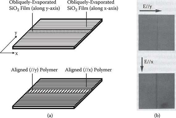
FIGURE 3.46 Control of polymer wire directions by stacked obliquely evaporated SiO2 films. (a) Process and (b) microscopic image observation with polarized light. From T. Yoshimura, K. Motoyoshi, S. Tatsuura, W. Sotoyama, A. Matsuura, and T. Hayano, “Selectively aligned polymer film growth on obliquely evaporated SiO2 pattern by chemical vapor deposition,” Jpn. J. Appl. Phys. 31, L980–L982 (1992).
To examine the birefringence induced by the aligned polymer wires, microscopic image observation under the cross-nicol condition was carried out using the setup shown in Figure 3.47. As Figure 3.48 shows, in the poly-AM film on the stripe pattern of SiO2 obliquely evaporated with θ = 45°, a bright 10-µm-wide stripe is observed, indicating that birefringence occurs selectively on the obliquely-evaporated SiO2 film. In the case of θ = 0°, no birefringence is observed. Estimation based on absorption spectra fringes revealed that the refractive index is about 1.65 for polarization perpendicular to the poly-AM wires and 1.95 for polarization parallel to the poly-AM wires. Using the anisotropicity of the refractive index, optical waveguides can be constructed without etching, and various other functional photonic devices will be realized. An investigation on a possibility of TFTs of feature sizes of 10 nm is also attractive.
Figure 3.49 shows microscopic images under the cross-nicol condition for polyimide grown with θ = 45° from PMDA and DDE by the same process as described previously for poly-AM. When the y-direction of the sample is perpendicular to the polarization direction of the incident light, the whole area of the sample is dark. When the sample is rotated and the y-direction of the sample deviates from the direction perpendicular to the polarization direction, similar to the case of poly-AM, a bright 10-µm-wide stripe is observed. This indicates that birefringence occurs selectively on the obliquely-evaporated SiO2 region, demonstrating that selectively-aligned growth is applicable to polyimide systems.
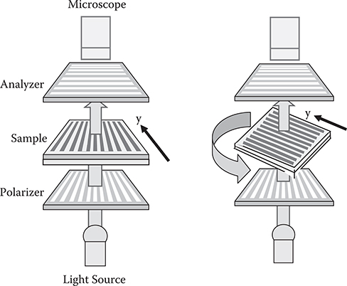
FIGURE 3.47 A setup for microscopic image observation under the cross-nicol condition. From K. Matsumoto and T. Yoshimura, “Electro-optic waveguides with conjugated polymer films fabricated by the carrier-gas-type organic cvd for chip-scale optical interconnects,” Proc. SPIE 6899, 98990E-1-9 (2008).
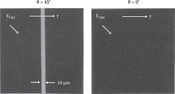
FIGURE 3.48 Microscopic images under the cross-nicol condition for poly-AM grown by selectively-aligned growth with θ = 45° and 0°.
Figure 3.50 shows microscopic images for birefringence measurement in poly-AM grown by the carrier gas–type organic CVD on a 200-nm-thick SiO film that is obliquely evaporated by tilting along the y-axis [28]. Growth time was 20 min. During the film growth, molecular gas pressure was kept around 100 Pa. For light polarization parallel to the y-axis, the microscope image is dark. When the substrate is rotated by 45° from the initial configuration, the stripe region, where the SiO underlayer is deposited by oblique evaporation, is brighter than the surrounding region due to birefringence. The results of the microscope image observation revealed that poly-AM wires are selectively aligned along the y-axis on the SiO underlayer pattern, similar to the case of SiO2.
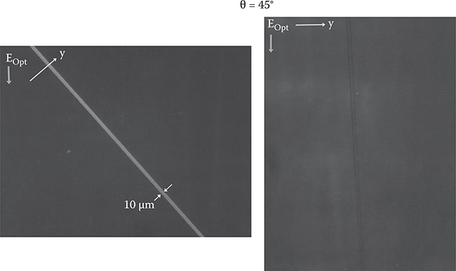
FIGURE 3.49 Microscopic images under the cross-nicol condition for polyimide grown by selectively-aligned growth with θ = 45°.
Observation of obliquely-evaporated SiO films for underlayers and poly-AM films was carried out by the atomic force microscope (AFM) [33]. As can be seen from Figure 3.51(a), in the obliquely-evaporated SiO film, a grain morphology along the y-axis is observed, revealing that the film has an anisotropic structure. In the poly-AM film on the obliquely-evaporated SiO film, as shown in Figure 3.51(b), line-shaped patterns along the y-axis are observed. This result suggests that polymer wires are aligned along the y-axis. In the glass substrate region, as shown in Figure 3.51(c), structures with definite orientation are not observed.
As described above, selectively-aligned growth is expected to be applicable to various kinds of polymers and can use various dielectric films for the underlayers.
3.6.3 ELECTRIC-FIELD-ASSISTED GROWTH
The concept of selectively-aligned growth with a strong electric field, which is called electric-field-assisted growth, using molecules A and B is shown in Figure 3.52. Here, at least one of the two kinds of molecules has electric dipoles. In the present case, molecule B has electric dipoles. Molecules A and B are provided onto a substrate surface, on which slit-type electrodes are formed. When molecule B comes near the surface, it tends to be aligned in the direction of the electric field generated between the electrodes. Since the molecular alignment is induced before the molecules are tightly inserted into polymer wires, the resistance against molecular rotation is small and molecules can be aligned without raising temperatures above glass transition temperature. It is expected that polymer wires, in which molecule B tends to have unique orientation, grow in a direction parallel to the electric field, achieving electric-field-assisted growth. In addition, in this growth method, little contamination is involved because no solvent is used and impurities in sources and by-products are easily removed in vacuum.
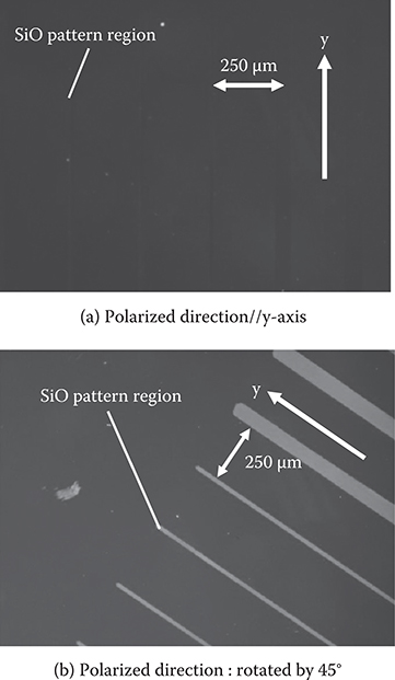
FIGURE 3.50 Microscopic images under the cross-nicol condition for poly-AM grown by the carrier gas–type organic CVD on obliquely-evaporated SiO film. From K. Matsumoto and T. Yoshimura, “Electro-optic waveguides with conjugated polymer films fabricated by the carrier-gas-type organic CVD for chip-scale optical interconnects,” Proc. SPIE 6899, 98990E-1-9 (2008).
Experimental demonstration of electric-field-assisted growth was performed for polyamic acid [PMDA/DNB] by using PMDA (molecule A) and DNB (molecule B) [34]. The reaction between PMDA and DNB is described in Section 3.3.1 (Figure 3.8). These molecules were evaporated separately from temperature-controlled K cells in a vacuum chamber to provide the molecules onto a glass substrate surface. The background pressure was 5 × 10⁻⁶ Pa. A slit-type electrode with a 10-µm gap was formed on the substrate. An electric field of 0.78 MV/cm for aligning the molecules was applied to the gap during film deposition.
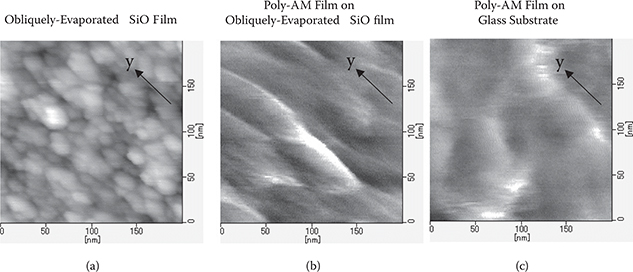
FIGURE 3.51 Atomic force microscope (AFM) images of obliquely-evaporated SiO film and poly-AM films. From Y. Suzuki, H. Kazama, N. Terasawa, Y. Naito, T. Yoshimura, Y. Arai, and K. Asama, “Selective growth of conjugated polymer thin film with nano scale controlling by chemical vapor depositions (CVD) toward ‘Nanonics,’” Proc. SPIE 5938, 59310G-1-8 (2005).
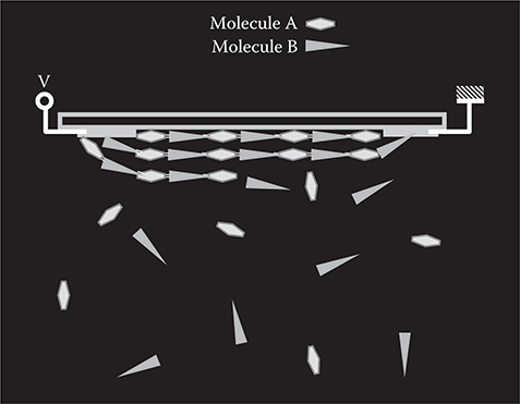
FIGURE 3.52 Selectively-aligned growth with a strong electric field—electric-field-assisted growth. From T. Yoshimura, Trends in Thin Solid Films Research (ed. A. R. Jost) Ch. 5 “Self-Organized Growth of Polymer Wire Networks with Designed Molecular Sequences for Wavefunction-Controlled Nano Systems.” Nova Science Publishers, New York (2007).
Table 3.1 shows the substrate temperature dependence of deposition rate and film appearance. Infrared (IR) measurements revealed that films show many characteristic polyamic acid absorption lines in the wavenumber region of 1000–2000 cm−1. We also found that the films become insoluble in methanol after being annealed at 220°C for 3 h. These results confirm that the as-deposited films are polyamic acid, which turns to polyimide by annealing. At Ts = 25°C, the films are not clear but at Ts = 65°C and 110°C they are clear.
Figure 3.53 shows the effect of co-evaporation on the film deposition rate. At Ts = 25°C, for supplying PMDA only, DNB only, or both, considerable deposition rates are detected. Residual molecules having no connection with polymer wires form island-like aggregates, resulting in a frosted film. For Ts = 65 and 110°C, the deposition rates are very low, owing to re-evaporation from the substrate when only PMDA or DNB is supplied. When co-evaporating PMDA and DNB together, the reaction on the substrate reduces the total vapor pressure, and the deposition rate is therefore increased by mass action. This indicates that residual molecules are removed automatically, forming a stoichiometric clear polymer film.
TABLE 3.1
Substrate Temperature Dependence of Deposition Rate and Film Appearance
Ts (°c) |
Gas Pressure (pa) |
Deposition Rate (nm/min) |
Film Appearance |
25 |
6 × 10⁻⁴ |
25 |
Frosted |
65 |
3 × 10⁻³ |
12 |
Clear |
110 |
3 × 10⁻³ |
5 |
Clear |
Source: T. Yoshimura, S. Tatsuura, and W. Sotoyama, “Chemical vapor deposition of polyamic acid thin films stacking non-linear optical molecules aligned with a strong electric field,” Thin Solid Films 207, 9–11 (1992).
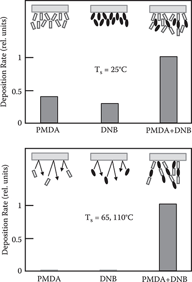
FIGURE 3.53 Effect of co-evaporation on the film deposition rate. From T. Yoshimura, S. Tatsuura, and W. Sotoyama, “Chemical vapor deposition of polyamic acid thin films stacking nonlinear optical molecules aligned with a strong electric field,” Thin Solid Films 207, 9–11 (1992).
Figure 3.54(a) shows the transmission spectra for the polyamic acid film deposited at Ts = 65°C and for methanol solutions of PMDA and DNB. The film shows an absorption band near a band in the spectrum of DNB, confirming that DNB molecules are inserted into the polymer wire. The splitting of the band might be attributed to a change in the electronic state in DNB in the wires. Figure 3.54(b) shows the absorption spectra of the film deposited at Ts = 65°C in the region between electrodes. The film is 160 nm thick. The absorption for polarization in the direction of the electric field applied during film deposition is slightly larger than that for polarization perpendicular to the electric field direction, suggesting that DNB molecules can be aligned by electric-field-assisted growth. This would make subsequent poling with heating unnecessary. It should be noted that direct polyimide film formations with molecules having electric dipoles would be possible by growth at a high substrate temperature.
Molecules having electric dipoles like DNB exhibit large second-order nonlinear optical properties. In the case of DNB, the second-order optical nonlinearity arises from the amino group acting as the electron donor and the nitro group acting as the electron acceptor. Poled polymer thin films containing such nonlinear optical molecules have been developed for electro-optic (EO) devices, but they have two serious problems—relaxation in the field-induced alignment of the nonlinear optical molecules and the insufficient EO coefficient of poled polymers.
The EO coefficient r of poled polymers obtained so far has been comparable to that of LiNbO3, and not much higher than LiNbO3. Nonlinear optical molecules with a large nonlinearity, for example, long conjugated molecules, are required to enhance r. To improve molecular alignment, we must reduce the resistance against electric-field-induced molecular rotation in poling, decrease the poling temperature, and increase the poling electric field. Conventionally poling is done in a rubber condition at a high temperature after the film is formed by spin coating. The surrounding polymer matrix prevents molecules, especially long ones with a large nonlinearity, from rotating smoothly. Thermal disturbance also degrades molecular alignment. High Tg polymers require a high temperature, which may destroy molecules. Spin-coated films also tend to contain contamination, which reduces the electric field.
Electric-field-assisted growth would resolve all these problems of the conventional method for poled polymer fabrication since it is a solvent/contamination-free process and it enables easy molecular alignment at low temperatures before the molecules are inserted into polymer wires.
3.6.4 HEAD-TO-TAIL GROWTH
The concept of the head-to-tail growth is shown in Figure 3.55. Here, a source molecule has two kinds of reactive groups at the head and tail positions. Chemical reactions selectively occur between the two kinds of groups. By providing the molecules onto a substrate surface, it is expected that polymer wires grow in a unique head-to-tail configuration. This method might be effective to enhance nonlinear optical properties in polymer wires. For head-to-tail growth, special molecules are necessary to carry out experimental demonstrations.
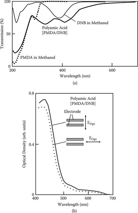
FIGURE 3.54 (a) Transmission spectra of PMDA, DNB, and polyamic acid [PMDA/DNB] deposited at TS = 65°C, and (b) absorption spectra of the polyamic acid film for polarized light in the region between electrodes. From T. Yoshimura, S. Tatsuura, and W. Sotoyama, “Chemical vapor deposition of polyamic acid thin films stacking non-linear optical molecules aligned with a strong electric field,” Thin Solid Films 207, 9–11 (1992).
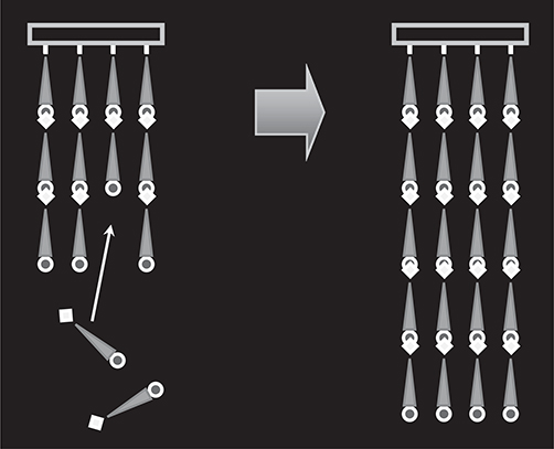
FIGURE 3.55 Head-to-tail growth. From T. Yoshimura, Trends in Thin Solid Films Research (ed. A. R. Jost) Ch. 5 “Self-Organized Growth of Polymer Wire Networks with Designed Molecular Sequences for Wavefunction-Controlled Nano Systems.” Nova Science Publishers, New York (2007).
3.7 Mass Production Process for Nano-Scale Devices Fabricated by MLD
In order to reduce the cost of thin-film organic photonic/electronic devices consisting of polymer wires grown by MLD, a mass production process is required. To do this, we proposed molecular nano duplication (MND), as shown in Figure 3.56 [23]. On a growth substrate, surface treatment such as SAM formation is applied in designed nano-scale patterns. On the SAM, removable molecules that have removable bonds connected to the SAM are placed by MLD, followed by polymer wire growth. After attaching a picking-up substrate on the surface, the removable bonds are cut by a chemical agent to separate the polymer wires from the SAM. Thus, nano-scale patterns consisting of polymer wires are transferred onto the picking-up substrate. Since the growth substrate with patterned SAM is reusable, further nano lithography is not required for nano-scale pattern duplication. By combining MND with selectively occupied repeated transfer (SORT) [35], which is described in Section 7.5, a material-saving mass production process will be provided.
3.8 Examples of Goals Achieved by MLD
By combining MLD with seed-core-assisted growth or the selective wire growth, various kinds of thin-film organic photonic/electronic devices and molecular nano systems will be constructed [2,3]. In the present section, some examples of the goals of MLD are briefly described.
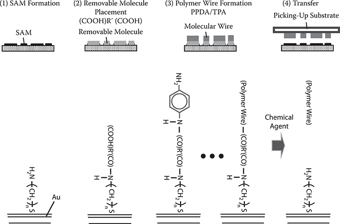
FIGURE 3.56 Molecular nano duplication. From T. Yoshimura, Y. Suzuki, N. Shimoda, T. Kofudo, K. Okada, Y. Arai, and K. Asama, “Three-dimensional chip-scale optical interconnects and switches with self-organized wiring based on device-embedded waveguide films and molecular nanotechnologies,” Proc. SPIE 6126, 612609-1-15 (2006).
3.8.1 FUNCTIONAL ORGANIC DEVICES
Figure 3.57 shows examples of various functional organic devices consisting of conjugated polymer wires grown by MLD with seed-core-assisted growth or the selective wire growth. For comparison, conventional devices consisting of random polymer wires fabricated by spin coating are illustrated. In electro-optic devices, polymer wires with controlled molecular sequences are grown in a definite direction parallel to the driving electric fields, which enhance the optical nonlinearity of EO waveguides. In photo-refractive device, in which photoconductive agents and carrier traps are added to the EO material, the same effect is expected. In electroluminescent (EL) devices and photovoltaic devices, polymer wires, in which a p-type region and an n-type region are formed in each polymer wire, are aligned from the lower electrode to the upper electrode. This structure improves carrier mobility in the devices. In electrochromic devices, p-type and n-type electrochromic molecules, and electron-blocking molecules are arranged in a polymer wire in this sequence. The configuration is suitable to generate color centers with trapped electrons arising from electric-field-induced polarization. In TFTs, the polymer wires are aligned from source to drain electrodes. This configuration improves carrier mobility in the polymer wires. When feature sizes less than 10 nm are required, seed cores made by nano lithography, such as electron beam lithography and scanning tunneling microscopy (STM), can be applied.
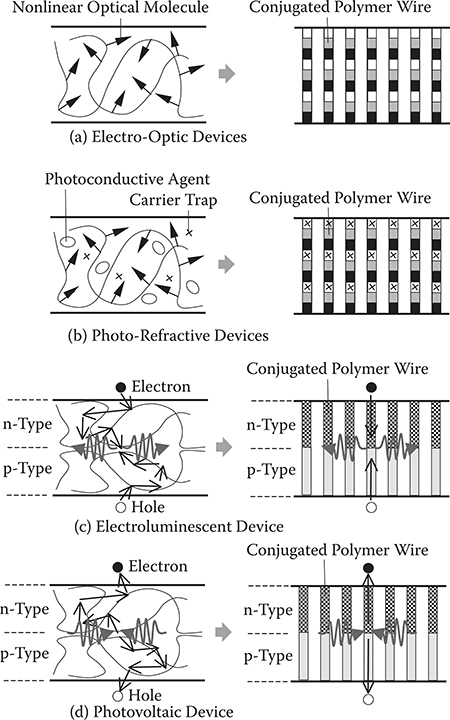
FIGURE 3.57 Examples of various functional organic devices consisting of conjugated polymer wires and improvement of the device performance by MLD with seed-core-assisted growth or selective wire growth.
3.8.2 INTEGRATED NANO-SCALE OPTICAL CIRCUITS
MLD with combining MND is preferable for constructing integrated nano-scale optical circuits consisting of high-index contrast (HIC) waveguides and photonic crystals. Low-cost mass production for heterogeneous integration of nano-scale optical circuits might be realized by using photolithographic packaging with SORT (PL-Pack with SORT) [35], whose details are described in Section 7.5. SORT is a resource-saving heterogeneous integration process with multistep device transfers using all-photolithographic methods without conventional flip-chip assembly packaging. Figures 3.58 and 3.59 show proposals of the nano-scale optoelectronic (OE) packaging [23]. In Figure 3.58, HIC waveguides are grown on a substrate with patterned SAM by MLD. The waveguides are picked up onto a picking-up substrate by MND. The waveguides
When the nano-scale optical circuits are used for chip-scale optical interconnects, the circuits are distributed with a pitch of ~100 μm corresponding to pad pitch of LSI chips. In this case, since the sizes of the nano-scale optical circuits are in the order of 10 μm, the optical circuits exist with very low density in the interconnect systems. SORT, in which the nano-scale optical circuits fabricated in dense two-dimensional arrays are distributed to necessary sites, enables us to save materials and process costs for the nano-scale optical circuit integration.
3.8.3 MOLECULAR CIRCUITS
High carrier mobility characteristics of their π-conjugated systems
Small wire diameter, which is smaller than that of carbon nanotubes.
Molecular sequence controllability in the wire with monomolecular scale, that is, precise wavefunction shape controllability, which is not available in carbon nanotubes.
FIGURE 3.58 SORT process with MND for transfers of nano-scale optical circuits. From T. Yoshimura, Y. Suzuki, N. Shimoda, T. Kofudo, K. Okada, Y. Arai, and K. Asama, “Three-dimensional chip-scale optical interconnects and switches with self-organized wiring based on device-embedded waveguide films and molecular nanotechnologies,” Proc. SPIE 6126, 612609-1-15 (2006).
FIGURE 3.59 Heterogeneous integration of nano-scale optical circuits using SORT. From T. Yoshimura, Y. Suzuki, N. Shimoda, T. Kofudo, K. Okada, Y. Arai, and K. Asama, “Three-dimensional chip-scale optical interconnects and switches with self-organized wiring based on device-embedded waveguide films and molecular nanotechnologies,” Proc. SPIE 6126, 612609-1-15 (2006).
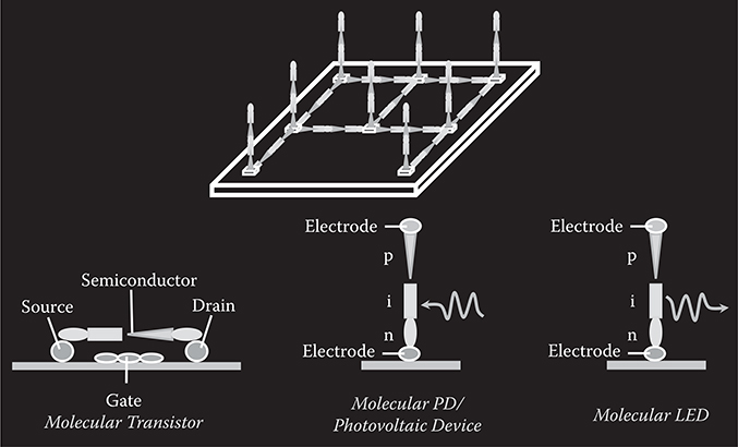
FIGURE 3.60 Concept of molecular circuits consisting of molecular transistors, PDs, photovoltaic devices, and LEDs. From T. Yoshimura, Trends in Thin Solid Films Research (ed. A. R. Jost) Ch. 5 “Self-Organized Growth of Polymer Wire Networks with Designed Molecular Sequences for Wavefunction-Controlled Nano Systems.” Nova Science Publishers, New York (2007).
The molecular circuits consist of molecular lines/electrodes, molecular transistors, molecular photodiodes (PDs), molecular photovoltaic devices, and molecular light-emitting diodes (LEDs). In order to construct the molecular circuits, the self-organized growth of the polymer/molecular wire network described in Section 3.4 is effective.
In molecular transistors, a semiconductor conjugated polymer wire is aligned from a source electrode to a drain electrode, passing above a gate electrode. Molecular PDs, photovoltaic devices, and LEDs are made of conjugated polymer wires with pin junctions that are sandwiched by a pair of conjugated polymer wires for electrodes.
Figure 3.61 shows tentative examples of conjugated polymer wires with pin junctions. For the donor/acceptor substitution-type pin junctions, donors and acceptors are respectively substituted in the p-type region and the n-type region. For the backbone-type pin junction, an n-type backbone and a p-type backbone are connected. In the tentative examples, poly-AM and poly-OXD are assumed for the backbones to make a junction. Although p- and n-type characterizations of poly-AM and poly-OXD are uncertain, if poly-AM and poly-OXD are formed within a polymer wire with molecular sequence arrangements like ABABABABADCDCDCDCD using the reactions shown in Figure 3.12 with molecule A: OA, molecule B: ODH, molecule C: TPA, and molecule D: PPDA, some kind of pin-like junctions might be formed in the poly-OXD–poly-AM interface region. For LED operation, electrons and holes are combined in the intrinsic, i, region under a forward bias condition to emit light beams. For PD operation, electrons and holes are generated by absorbing light in the i region under a backward bias condition to induce currents and voltage. Photovoltaic operation is also available in the same structure as the PD.
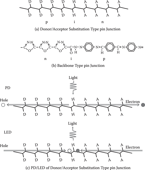
FIGURE 3.61 Tentative examples of conjugated polymer wires with pin junctions. From T. Yoshimura, Trends in Thin Solid Films Research (ed. A. R. Jost) Ch. 5 “Self-Organized Growth of Polymer Wire Networks with Designed Molecular Sequences for Wavefunction-Controlled Nano Systems.” Nova Science Publishers, New York (2007).
References
1. T. Yoshimura, S. Tatsuura, and W. Sotoyama, “Polymer films formed with monolayer growth steps by molecular layer deposition,” Appl. Phys. Lett. 59, 482–484 (1991).
2. T. Yoshimura, E. Yano, S. Tatsuura, and W. Sotoyama, “Organic functional optical thin film, fabrication and use thereof,” U.S. Patent 5,444,811 (1995).
3. T. Yoshimura, “Self-organized growth of polymer wire networks with designed molecular sequences for wavefunction-controlled nano systems,” in Trends in thin solid films research, edited by A. R. Jost. Nova Science Publishers, New York (2007).
4. T. Yoshimura, Molecular nano systems: Applications to optoelectronic computers and solar energy conversion, Corona Publishing Co., Ltd., Tokyo (2007) [in Japanese].
5. T. Yoshimura, “Liquid phase deposition,” Japanese Patent, Tokukai Hei 3-60487 (1991) [in Japanese].
6. T. Yoshimura, “Growth methods of polymer wires and thin films,” Japanese Patent Tokukai 2008-216947 (2008) [in Japanese].
7. T. Suntola, “Atomic layer epitaxy,” Material Science Reports 4(7) (1989).
8. M. Pessa, R. Makela, and T. Suntola, “Characterization of surface exchange reactions used to grow compound films,” Appl. Phys. Lett. 38, 131–133 (1981).
9. T. Yoshimura, S. Ito, T. Nakayama, and K. Matsumoto, “Orientation-controlled molecule-by-molecule polymer wire growth by the carrier-gas-type organic chemical vapor deposition and the molecular layer deposition,” Appl. Phys. Lett. 91, 033103-1–3 (2007).
10. T. Yoshimura and Y. Kudo, “Monomolecular-step polymer wire growth from seed core molecules by the carrier-gas type molecular layer deposition (MLD),” Appl. Phys. Express 2, 015502-1–3 (2009).
11. Y. Takahashi, M. Iijima, K. Inagawa, and A. Itoh, “Synthesis of aromatic polyimide film by vacuum deposition polymerization,” J. Vac. Sci. Technol. A 5, 2253–2256 (1987).
12. M. Iijima, Y. Takahashi, and E. Fukuda, “Vacuum deposition polymerization,” Nikkei New Materials, December 11, 93–100 (1989) [in Japanese].
13. M. Putkonen, J. Harjuoja, T. Sajavaara, and L. Niinisto, “Atomic layer deposition of polyimide thin films,” J. Mater. Chem., DOI:10.1039/b612823h Paper (2007).
14. L. Salmi, M. Vehkamaki, E. Puukilainen, and M. Ritala, “ALD of inorganic-organic nanolaminates,” AVS, 8th International Conference on Atomic Layer Deposition, WedM1b-2, Bruges, Belgium (2008).
15. S. M. George, B. Yoon, and A. A. Dameron, “Surface chemistry for molecular layer deposition of organic and hybrid organic-inorganic polymers,” Acc. Chem. Res. 42, 498–508 (2009).
16. X. Liang and A. Weimer, “Photoactivity passivation of TiO2 nanoparticles using molecular layer deposition (MLD) polymer films,” J. Nanopart. Res., DOI 10.1007/s11051-009-9587-0 (2009).
17. P. W. Loscutoff, H. Zhou, and S. F. Bent, “Molecular layer deposition of multicomponent organic films for nanoelectronics,” AVS, 9th International Conference on Atomic Layer Deposition, Monterey, California, 148 (2009).
18. H. Murata, S. Ukishima, H. Hirano, and T. Yamanaka, “A novel fabrication technique and new conjugated polymers for multilayer polymer light-emitting diodes,” Polymer for Advanced Technologies 8, 459–464 (1996).
19. T. Yoshimura, S. Tatsuura, W. Sotoyama, A. Matsuura, and T. Hayano, “Quantum wire and dot formation by chemical vapor deposition and molecular layer deposition of one-dimensional conjugated polymer,” Appl. Phys. Lett. 60, 268–270 (1992).
20. K. Kiyota, T. Yoshimura, and M. Tanaka, “Electrophotographic behavior of ZnO sensitized by two dyes,” Photogr. Sci. Eng. 25, 76–79 (1981).
21. T. Yoshimura, K. Kiyota, H. Ueda, and M. Tanaka, “Contact potential difference of ZnO layer adsorbing p-type dye and n-type dye,” Jpn. J. Appl. Phys. 18, 2315–2316 (1979).
22. H. Kokado, T. Nakayama, and E. Inoue, “A new model for spectral sensitization of photoconduction in zinc oxide powder,” J. Phys. Chem. Solids 34, 1–8 (1973).
23. T. Yoshimura, Y. Suzuki, N. Shimoda, T. Kofudo, K. Okada, Y. Arai, and K. Asama, “Three-dimensional chip-scale optical interconnects and switches with self-organized wiring based on device-embedded waveguide films and molecular nanotechnologies,” Proc. SPIE 6126, from Photonics West 2006, San Jose, California, 612609- 1-15 (2006).
24. D. Seghete, B. Yoon, A. S. Cavanagh, and S. M. George, “New approaches to molecular layer deposition using ring-opening and heterobifunctional reactants,” AVS, 8th International Conference on Atomic Layer Deposition, WedM1b-3, Bruges, Belgium (2008).
25. Private comment from Dr. E. Liskola in AVS, 8th International Conference on Atomic Layer Deposition, Bruges, Belgium (2008).
26. M. Iijima and Y. Takahashi, “Techniques for vapor deposition polymerization: Preparation of organic functional thin films,” OYO BUTURI 66, 1084–1088 (1997) [in Japanese].
27. D. Kim and T. Yoshimura, “The domain-isolated molecular layer deposition (DI-MLD) for fast polymer wire growth,” AVS, 9th International Conference on Atomic Layer Deposition, Monterey, California, 243 (2009).
28. K. Matsumoto and T. Yoshimura, “Electro-optic waveguides with conjugated polymer films fabricated by the carrier-gas-type organic CVD for chip-scale optical interconnects,” Proc. SPIE 6899, from Photonics West 2008, San Jose, California, 98990E- 1-9 (2008).
29. T. Yoshimura, N. Terasawa, H. Kazama, Y. Naito, Y. Suzuki, and K. Asama, “Selective growth of conjugated polymer thin films by the vapor deposition polymerization,” Thin Solid Films 497, 182–184 (2006).
30. T. Kanetake, K. Ishikawa, T. Koda, Y. Tokura, and K. Takeda, “Highly oriented polydiacetylene films by vacuum deposition,” Appl. Phys. Lett. 51, 1957–1959 (1987).
31. J. S. Patel, S. D. Lee, G. L. Baker, and J. A. Shelburne, “Epitaxial growth of aligned polydiacetylene films on anisotropic orienting polymers,” Appl. Phys. Lett. 56, 131–133 (1990).
32. T. Yoshimura, K. Motoyoshi, S. Tatsuura, W. Sotoyama, A. Matsuura, and T. Hayano, “Selectively aligned polymer film growth on obliquely evaporated SiO2 pattern by chemical vapor deposition,” Jpn. J. Appl. Phys. 31, L980–L982 (1992).
33. Y. Suzuki, H. Kazama, N. Terasawa, Y. Naito, T. Yoshimura, Y. Arai, and K. Asama, “Selective growth of conjugated polymer thin film with nano scale controlling by chemical vapor depositions (CVD) toward ‘Nanonics,’” Proc. SPIE 5938, from Optics & Photonics 2005, San Diego, California, 59310G- 1–8 (2005).
34. T. Yoshimura, S. Tatsuura, and W. Sotoyama, “Chemical vapor deposition of polyamic acid thin films stacking non-linear optical molecules aligned with a strong electric field,” Thin Solid Films 207, 9–11 (1992).
35. T. Yoshimura, M. Ojima, Y. Arai, and K. Asama, “Three-dimensional self-organized micro optoelectronic systems for board-level reconfigurable optical interconnects: Performance modeling and simulation,” IEEE J. Select. Topics in Quantum Electron. 9, 492–511 (2003).