9 Applications to Solar Energy Conversion Systems
This chapter presents expected applications of molecular layer deposition (MLD) and related thin-film organic photonic/electronic materials to solar energy conversion systems. Applications to photosynthesis devices are also discussed.
9.1 Sensitized Photovoltaic Devices
We propose multidye sensitization and polymer-MQD (multiple quantum dot) sensitization for photovoltaic devices. In the former, the sensitizing layer consists of molecular wires in which a plurality of kinds of dye molecules are stacked with designated sequences by liquid-phase MLD. In the latter, the sensitizing layer consists of polymer MQDs grown by gas-phase MLD. We also propose waveguide-type photovoltaic devices, which enhance light absorption of the sensitizing layers.
In the present section, after details of the proposed concepts are described, several experimental proofs of concept are demonstrated.
9.1.1 CONCEPT OF MULTIDYE SENSITIZATION AND POLYMER-MQD SENSITIZATION
Structures for multidye sensitization and polymer-MQD sensitization are shown in Figure 9.1. In multidye sensitization [1, 2 and 3], molecular wires consisting of dye molecules are grown on a semiconductor surface. In the example shown in Figure 9.1(a), four different kinds of molecules are stacked on a surface. In polymer-MQD sensitization [1, 2, 3 and 4], polymer wires having MQDs with different dot lengths are grown on a semiconductor surface. In the example shown in Figure 9.1(b), four MQDs of different lengths are contained in a polymer wire. The polymer wire directions can be vertical or horizontal.
When Si is used for the semiconductor, as illustrated in Figure 9.2(a), the band gap of Si is relatively narrow, and therefore the photon energy of visible ultraviolet light is much larger than the band gap. In such a case, excess energy of photons is lost as heat, which reduces the light energy conversion efficiency of the Si solar cells.
When multidye-sensitized ZnO with molecular wires consisting of p-type and n-type dye molecules is used for the semiconductor, the energy diagrams and absorption spectra can be drawn as in Figure 9.2(b) [5]. In this example, four kinds of dye molecules are aligned in a p/n/p/n sequence on the n-type ZnO. Since dye molecules have narrow absorption bands as compared with ordinary semiconductors, by appropriate selection of dye molecules, the absorption wavelength region from near-infrared to visible can be divided using several kinds of dye molecules. Each kind of dye molecule absorbs light with wavelengths matched to its own energy gap and injects the excited electrons into the ZnO. This might suppress the energy loss arising from the excess photon energy. The structure is regarded as a molecular tandem structure. Such molecular wire structures are grown by MLD described in Sections 3.1.1 and 3.1.2. In some cases, it is also possible to use “MLD with molecule groups” described in Section 3.1.3. For example, Molecule Group I containing p-type molecules 1 and 3, and Molecule Group II containing n-type molecules 2 and 4, are prepared. By supplying Molecule Group I and Molecule Group II sequentially, structures of molecular wires 1/2, 1/4, 3/2, 3/4 are grown simultaneously. This enables us to realize the four-divided light absorption scheme shown in Fig. 9.2(b) by two-dye molecular wires grown by two-step MLD instead of four-dye molecular wires grown by four-step MLD.
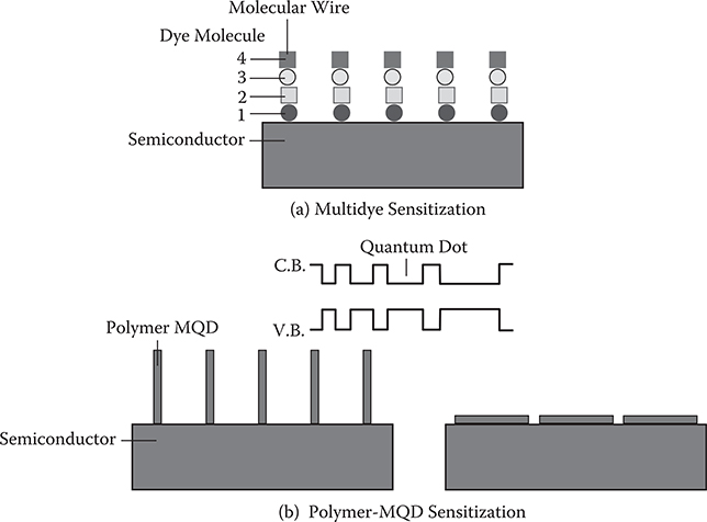
FIGURE 9.1 Multidye sensitization and polymer-MQD sensitization.

FIGURE 9.2 Schematic illustrations of energy levels and absorption spectra in (a) Si, (b) multidye-sensitized ZnO, and (c) polymer-MQD-sensitized ZnO.
When the polymer-MQD-sensitized ZnO is used for the semiconductor, the same effect might be obtained as in the multidye-sensitized ZnO. The energy diagrams and absorption spectra are drawn in Figure 9.2(c). Absorption bands of quantum dots are narrow as compared with ordinary semiconductors and the absorption peak energy is controlled by the quantum dot length. Therefore, by adjusting the quantum dot lengths in the polymer wire appropriately, the absorption wavelength region can be divided using quantum dots with different lengths. Each quantum dot absorbs light with wavelengths matched to its own energy gap and injects the excited electrons into the ZnO.
We propose two more multidye sensitization processes, which utilize processes similar to the photosynthesis process in plants. In the process shown in Figure 9.3(a), gradual energy steps are formed in the molecular wire, which is similar to the electron transporting system in the z-scheme of the photosynthesis process, to perform smooth electron transfer to the ZnO. In the process drawn on the left, the electron transfer from the redox system occurs at the top of the molecular wire. In the process drawn on the right, it occurs at the inner part of the molecular wires.
In the process shown on the left in Fig. 9.3(b), the z-scheme-like molecular arrangements are formed. In this example, an electron excited from a highest occupied molecular orbital (HOMO) of molecule 1 by a photon with a wavelength of λ1 is transferred into the ZnO. An electron excited by a photon with λ2 in molecule 2 is transferred to the HOMO of molecule 1 to compensate the hole left in the HOMO. The hole left in the HOMO of molecule 2 is compensated by a redox system. In the process shown on the right in Fig. 9.3(b), an electron excited by a photon with a wavelength of λ2 in molecule 2 is transferred into the ZnO via molecule 1. An electron excited by a photon with λ4 in molecule 4 is transferred to the highest occupied molecular orbital (HOMO) of molecule 2 via molecule 3. The hole left in molecule 4 is compensated by a redox system. A similar same electron flow can be generated when an electron is excited by a photon with λ1 in molecule 1 instead of in molecule 2, and when an electron is excited by a photon with λ3 in molecule 3 instead of in molecule 4.
The sensitization mechanism with z-scheme-like molecular arrangements has following two advantages.
It increases the difference in energy between the Fermi level of ZnO and the electrode potential of the redox system to increase the generated voltage in the photovoltaic device.
It suppresses the energy loss arising from the excess photon energy, which occurs in Si photovoltaic devices, to improve the light energy conversion efficiency.
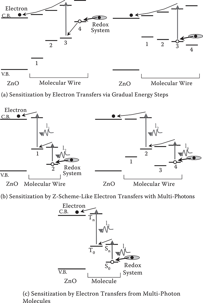
FIGURE 9.3 Proposed molecular arrangements of molecular wires on ZnO for sensitization utilizing the photosynthesis process. Sensitization by (a) electron transfers via gradual energy steps, and (b) z-scheme-like electron transfers with multiphotons, and (c) by electron transfers from molecules with four-level two-photon absorption capability.
For the z-scheme-like molecular arrangements, a molecule with HOMO of a high energy level and a molecule with LUMO of a low energy level should be combined. For example, the former could be crystal violet, piacyanol etc., and the latter could be phthalocyanine, C60 etc.
The above-mentioned molecular wire structures are grown by MLD described in sections 3.1.1, 3.1.2, or “MLD with molecule groups” described in section 3.1.3.
The similar sensitization as the z-scheme-like electron transfer might arise from molecules with multi-photon absorption characteristics. The concept of the four-level two-photon absorption is shown in Fig. 9.3(c). A photon with a wavelength of λ1 excites an electron from singlet S0 state to Sn state in a molecule, and the excited electron in Sn state transfers to triplet T0 state. Then, a photon with another wavelength of λ2 further excites the electron to Tn state to complete the four-level two-photon absorption [6,7]. The transfer of the excited electron to the conduction band of ZnO generates photocurrents. Protoporphyrin, tetraphenylporphyrin, biacetyl, comphorquinone, benzyl, etc. are known as two-photon-absorption materials [6,7].
9.1.2 WAVEGUIDE-TYPE PHOTOVOLTAIC DEVICE CONCEPT
Dye-sensitized photovoltaic devices [8] have attracted much attention as cost-effective solar energy conversion modules. In Figure 9.4, the conventional dye-sensitized solar cell and the waveguide-type dye-sensitized photovoltaic device are compared. In the conventional device shown in Figure 9.4(a), in order to increase the number of adsorbed dye molecules on semiconductor surfaces, porous semiconductors are used. In this case, although sufficient light absorption is accomplished for normally incident light into the semiconductor surfaces, the crystalline quality of semiconductors tends to become poor, suppressing electron mobility. Furthermore, the porous structure narrows the electron transport channels. Consequently, the internal resistivity increases to degrade the photovoltaic performance in the conventional dye-sensitized solar cell.
In the waveguide-type dye-sensitized photovoltaic device shown in Figure 9.4(b) [2,4], on the other hand, thin film semiconductors with flat surfaces and high crystalline quality, that is, high electron mobility, are used. So, the internal resistivity decreases to improve photovoltaic performance. However, in this case, the number of adsorbed dye molecules on the semiconductor surfaces is insufficient. Because normally incident light into the devices passes through only a mono layer of dye molecules, very little light absorption is available. To resolve this problem, instead of normally incident light, guided light is used in semiconductor thin films. In this configuration, light beams pass through a lot of dye molecules to enhance light absorption. Thus, high-performance dye-sensitized photovoltaic devices will be realized. If necessary, transparent electrodes can be replaced with metal electrodes, which will reduce material costs and series internal resistance of electrodes.
Figure 9.4(c) shows a waveguide-type photovoltaic device with multidye sensitization and polymer-MQD sensitization. To form the sensitizing layer, molecular wires containing dye molecules or polymer MQDs are grown on a thin-film semiconductor surface. The electrolyte is located between the semiconductor and the counter electrode. A solid-state electrolyte is preferable for film-shaped devices. The electrolyte can also be replaced with a thin-film semiconductor to form this structure: n-type semiconductor/sensitizing layer/p-type semiconductor. The light beam is guided in the layered structures.
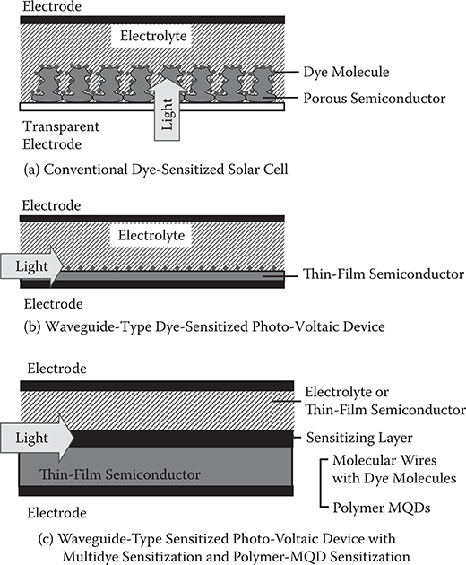
FIGURE 9.4 Comparison of (a) the conventional dye-sensitized solar cell and (b) the waveguide-type dye-sensitized photovoltaic device. (c) The waveguide-type sensitized photovoltaic device with multidye sensitization and polymer-MQD sensitization. From T. Yoshimura, A. Oshima, D. Kim, and Y. Morita, “Quantum dot formation in polymer wires by three-molecule molecular layer deposition (MLD) and applications to electro-optic/photovoltaic devices,” ECS Transactions 25, No. 4 “Atomic Layer Deposition Applications 5,” 15–25 (2009).
A serious issue for waveguide-type photovoltaic devices is optical coupling. Some of the candidates for coupling methods are shown in Figure 9.5. One of the promising ways is to embed the photovoltaic device in waveguide-type light beam collecting films (described in Section 9.2). For the optical coupling between the photovoltaic devices and optical waveguides in the light beam collecting film, reflective SOLNET (R-SOLNET; described in Section 7.4) might be useful because a self-organized lightwave network (SOLNET) can connect optical waveguides with different mode sizes.
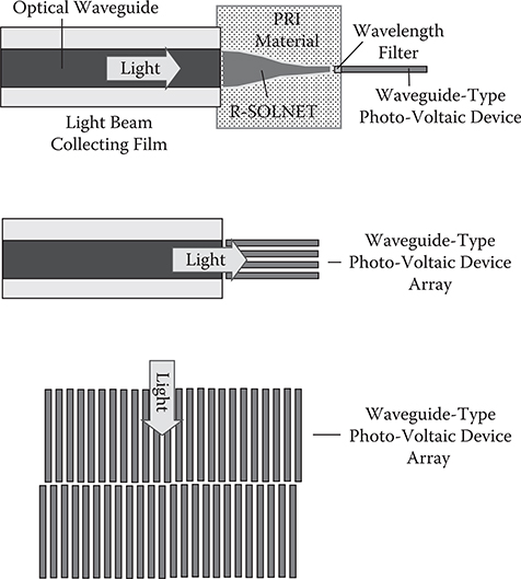
FIGURE 9.5 Possible optical coupling methods to introduce light beams into waveguide-type photovoltaic devices.
Another way utilizes arrays of waveguide-type photovoltaic devices. In this case, the light beams from the optical waveguides in the light beam collecting film can be coupled into the photovoltaic devices without SOLNET. The waveguide-type photo-voltaic device arrays can also be used in the normally incident light configuration by placing the array vertically. By stacking the arrays to form multilayered structures, the light beams passing through the arrays in the upper layers can be caught by the array in the lower layers to improve light energy conversion efficiency.
An example of the fabrication process of waveguide-type photovaoltaic device arrays is illustrated in Figure 9.6. A thin film of a semiconductor such as ZnO is grown on a transparent electrode layer having deep trenches with a high aspect ratio. As reported by H. Shin et al. [9], and as mentioned in Section 2.4, such a 3-D structure can be formed by atomic layer deposition (ALD). The sensitizing layer growth can be carried out by MLD [10,11]. Liquid-phase MLD [12,13] and gas-phase MLD [4,13] are respectively applied to the molecular wires of dye molecules and polymer MQDs. By supplying electrolytes to the thin film surface, a waveguide-type photo-vaoltaic device array with the structure in Figure 9.4(c) can be obtained.
It should be noted that the light beams propagating in both the electrolyte and semiconductor thin films can be used for waveguide-type photovoltaic devices. In this case, although light intensity in the semiconductor region is reduced, the tolerance of optical coupling to the waveguide-type photovoltaic device is considerably widened.
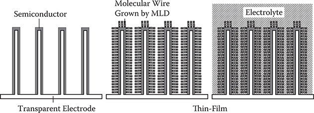
FIGURE 9.6 Fabrication process of a waveguide-type photovoltaic device array.
9.1.3 PROOF OF CONCEPT OF MULTIDYE SENSITIZATION BY LIQUID-PHASE MLD
As mentioned in Section 3.3.2, surface potential measurements revealed that, when p-type dye molecules and n-type dye molecules are coadsorbed simultaneously on n-type ZnO, dye molecules are self-assembled into the structure of n-type ZnO/p-type dye molecule/n-type dye molecule to form an npn structure (Figure 3.17) [14]. The structure is formed by the electrostatic force between dye molecules and between a dye molecule and ZnO. This indicates a possibility that MLD utilizing electrostatic force can be applied to growth of the molecular wires with p-type and n-type dye molecules in the multidye-sensitized photovoltaic device shown in Figure 9.1(a).
The spectral sensitization effect of the p/n-stacked structures on ZnO surfaces was first observed by Kiyota et al. in dyed ZnO for photoreceptors in electrophoto-graphic systems [15]. The sensitization mechanism in photovoltaic devices is similar to that in photoreceptors. Therefore, the p/n-stacked structures on ZnO are expected to be applied to photovoltaic devices.
This section presents sensitization of ZnO by stacked structures of p-type and n-type dye molecules, which are regarded as molecular wires consisting of two dye molecules. The section then describes widening of photocurrent spectra in ZnO sensitized by the p/n-stacked structures, which are formed by the liquid-phase MLD.
9.1.3.1 Spectral Sensitization of ZnO by p/n-Stacked Structures
Investigation of spectral sensitization by p/n-stacked structures was carried out by surface potential measurements [15] and photocurrent measurements [16].
The samples for measuring surface potential and photocurrent were prepared as follows. A ZnO layer (thickness: 20 µm, ZnO powder: Sakai Chem. Co. Sazex 2000 #) was first formed on a glass substrate with a slit-type SnO2 electrode (slit length: 10 mm, slit gap: 0.5 mm). For the adsorption of dye molecules, 0.01 mL of an alcohol solution (dye concentration: 1.6 × 10⁻³ mol/l) was dropped on the ZnO layer (area: 3 cm2). For the coadsorption of the two dye molecules, 0.01 mL of an alcohol solution containing the two kinds of dye in equal concentration (1.6 × 10⁻³ mol/l) was dropped on the ZnO layer.
Surface potential of the dyed ZnO surfaces were measured by a surface potentiometer. For photocurrent, 30 V was applied at the slit gap of the sample, which was illuminated by monochromatic light, and the current was measured by an electrometer. In the experiments, the following six dyes were used: fluorescein (FL), eosine (EO), and rose bengal (RB) as the p-type dye molecules, and crystal violet (CV), malachite green (MG), and brilliant green (BG) as the n-type dye molecules. The structures of the dye molecules are shown in Figure 3.14. Figure 9.7 shows the reflection spectra of the dyed ZnO. It was found that p-type dye molecules exhibit an absorption band in shorter wavelength regions as compared to the n-type dye molecules.
9.1.3.1.1 Surface Potential Variation Induced by Illumination [16]
In ZnO, zinc atoms in interstitial sites donate their electrons to oxygen adsorbed on the ZnO surface to form an electric double layer, causing a negative surface potential for the ZnO layer as shown in Figure 3.15. The surface potential of a ZnO layer that has adsorbed p-type dye molecules is more negative than that of an undyed ZnO layer [14] since the electrons in the ZnO layer are transferred to the p-type dye layer. Conversely, in the case of n-type dye molecules, the surface potential is less negative than that of an undyed ZnO layer [14] since the electrons in the n-type dye layer are transferred to the ZnO layer. When visible light falls on a dyed ZnO layer, the surface potential of the layer varies as shown in Figure 9.8(a). Here, ZnO/RB, ZnO/CV, and ZnO/MG indicate that the ZnO layer adsorbs RB, CV, and MG, respectively. The variation of the surface potential arises as follows.
The dye molecules absorb light and electron-hole pairs are generated in the dye molecules.
The electrons in the dye molecules are injected into the ZnO layer and the holes left in the dye molecules are compensated by the ionized oxygen on the ZnO surface.
Consequently, a decrease in the strength of the electric double layer at the ZnO surface is observed as the variation of the surface potential.
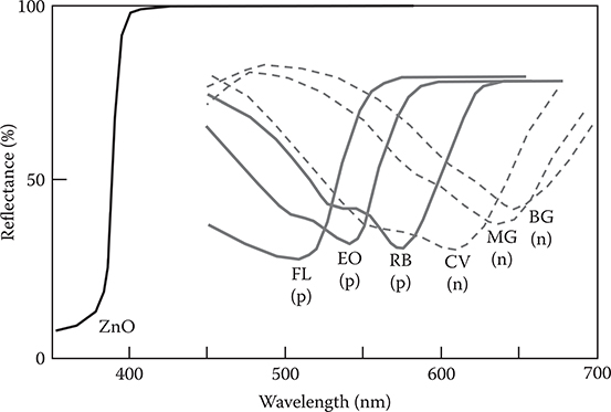
FIGURE 9.7 Reflection spectra of dyed ZnO.
As Figure 9.8(b) shows, when UV light illuminates the samples, the initial variation rates of the surface potentials are not dependent on the adsorbed dye molecules. This is because most of the UV light is transmitted through the dye layers and electron-hole pairs are generated in the ZnO.
As Figure 9.8(a) shows, variations of the surface potential of the samples illuminated by visible light depend heavily on the adsorbed dye molecules. In this case, the saturated values of the surface potential are determined by both the injection rate of the electrons from the dye molecules into the ZnO and the trapping rate of the electrons in the ZnO by adsorbed oxygen. Because the trapping rate does not depend on the adsorbed dye molecules, the results shown in Figure 9.8(a) indicate that the injection rates for RB, CV, and MG become, in that order, successively lower. We found that the saturated values become larger as the light intensity increases, which suggests that the larger the injection rate of the electrons becomes, the larger the saturated value becomes.
The initial variation rate of the surface potential, defined by (dV/dt)t=0 = (1/C)(dQ/ dt)t=0, is proportional to the injection rate of the electrons from the dye molecule to the ZnO layer. Here Q and C are the density of electric charge and the capacitance of the electric double layer at the ZnO surface, respectively.
Figure 9.9 shows the wavelength dependence of the initial slope of the surface potential variation, which is proportional to the injection rates. Here, ZnO/RB/CV indicates the sample of ZnO layer adsorbing the RB molecule and the CV molecule, in that order. Figure 9.10 shows the reflection spectra of ZnO/RB, ZnO/CV, and ZnO/RB/CV. It can be seen from Figures 9.9 and 9.10 that the maximum value of the spectrum of the electron injection rate in ZnO/CV is much smaller than that in ZnO/RB, while the peak height of the reflection spectrum of ZnO/CV is nearly equal to that of ZnO/RB. This indicates that the electron injection efficiency in sample ZnO/CV is lower than that in ZnO/RB.
In the case of ZnO/RB/CV, while the reflection spectrum is almost the same as that of ZnO/CV, the electron injection rate in ZnO/RB/CV is much larger than that in ZnO/CV. The electron injection efficiency from the CV molecule is raised by inserting the RB molecule between the ZnO and the CV molecule. Similar observations were obtained when MG was used instead of CV. This indicates that the electron injection efficiency from the n-type dye molecule to ZnO is enhanced by inserting a p-type dye molecule between the ZnO layer and the n-type dye molecule. This effect makes the multidye sensitization, in which p/n/p/n/… molecular wire structures are utilized as shown in Figures 9.1 and 9.2, viable.
9.1.3.1.2 Sensitization of Photocurrents [17]
Photocurrents in the dyed ZnO layers at the maximum absorption wavelengths of the adsorbed dye molecules are listed in Table 9.1 for dyes whose reflection spectra are shown in Figure 9.7. It can be seen that the photocurrents are much larger for the p-type dye molecules than for the n-type dye molecules, while the peak values of light absorption are almost the same for both p-type dye and n-type dye molecules. This confirms that the p-type dye molecule injects photocarriers into the ZnO layer more efficiently than the n-type dye molecule does, as H. Meier demonstrated [18]. The results are parallel to those obtained by surface potential measurements.
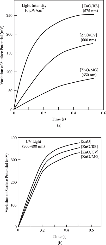
FIGURE 9.8 Variations of the surface potential of the dyed ZnO layer illuminated by (a) visible light, (b) UV light. From T. Yoshimura, K. Kiyota, H. Ueda, and M. Tanaka, “Influence of illumination on the surface potential of ZnO adsorbing p-type dye and n-type dye,” Jpn. J. Appl. Phys. 19, 1007–1008 (1980).

FIGURE 9.9 Wavelength dependence of the initial slope of the surface potential variation of the dyed ZnO layer. From T. Yoshimura, K. Kiyota, H. Ueda, and M. Tanaka, “Influence of illumination on the surface potential of ZnO adsorbing p-type dye and n-type dye,” Jpn. J. Appl. Phys. 19, 1007–1008 (1980).
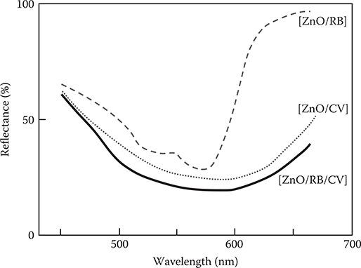
FIGURE 9.10 Reflection spectra of ZnO/RB, ZnO/CV, and ZnO/RB/CV. From T. Yoshimura, K. Kiyota, H. Ueda, and M. Tanaka, “Influence of illumination on the surface potential of ZnO adsorbing p-type dye and n-type dye,” Jpn. J. Appl. Phys. 19, 1007–1008 (1980).
TABLE 9.1
Photocurrents in Dyed zno Layers at the Maximum Absorption Wavelengths of the Dyes
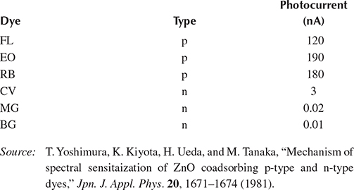
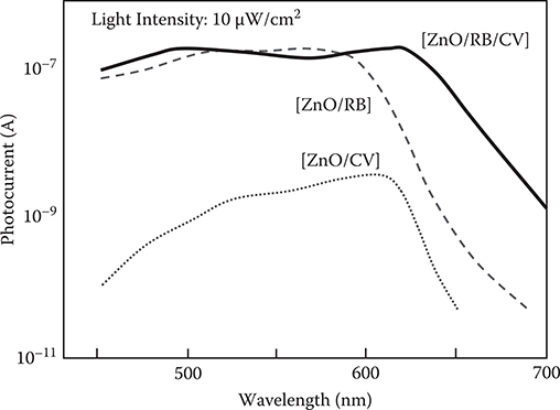
FIGURE 9.11 Spectral sensitization of ZnO/RB, ZnO/CV, and ZnO/RB/CV. From T. Yoshimura, K. Kiyota, H. Ueda, and M. Tanaka, “Mechanism of spectral sensitization of ZnO coadsorbing p-type and n-type dyes,” Jpn. J. Appl. Phys. 20, 1671–1674 (1981).
A typical spectral sensitization by the p/n-stacked structures is shown in Figure 9.11. Here, the p-type dye is RB and the n-type dye is CV. The photocurrents are for a light intensity of 10 µW/cm2. It is found that photocurrents in ZnO/RB/CV are much larger than in ZnO/RB and ZnO/CV in the 600 to 700 nm wavelength region. As Figures 9.12 and 9.13 show, the same kind of sensitization with two dyes is observed in ZnO/RB/MG and ZnO/EO/MG. In the 600 to 700 nm wavelength region, profiles of the photocurrent spectra for the ZnO layers with p/n-stacked structures are similar to the profiles of the reflection spectra of the n-type dyes adsorbed on the top.
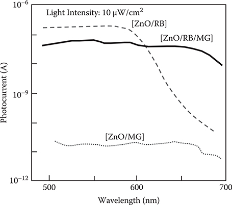
FIGURE 9.12 Spectral sensitization of ZnO/RB, ZnO/MG, and ZnO/RB/MG. From T. Yoshimura, K. Kiyota, H. Ueda, and M. Tanaka, “Mechanism of spectral sensitization of ZnO coadsorbing p-type and n-type dyes,” Jpn. J. Appl. Phys. 20, 1671–1674 (1981).

FIGURE 9.13 Spectral sensitization of ZnO/EO, ZnO/MG, and ZnO/EO/MG. From T. Yoshimura, K. Kiyota, H. Ueda, and M. Tanaka, “Mechanism of spectral sensitization of ZnO coadsorbing p-type and n-type dyes,” Jpn. J. Appl. Phys. 20, 1671–1674 (1981).
It should be noted that the photocurrent in ZnO/RB/MG is much larger than that in ZnO/EO/MG in the red light region, indicating that the degree of sensitization with p/n-stacked structures greatly depends on the combination of the two dyes.
Pioneering study on super spectral sensitization by two-molecule coadsorption was reported by Kokado et al. [19] and Hauffe [20]. The sensitization with the p/n-stacked structure reported here has a distinct advantage in that it will be able to extend toward multistacked structures consisting of molecules of more than three kinds because the structures might be fabricated by MLD utilizing electrostatic force.
9.1.3.1.3 Mechanism of Sensitization with p/n-Stacked Structures [17]
We have already clarified the following phenomena on sensitization with p/n-stacked structures:
Dramatic sensitization with dye-molecule-stacked structures arises only from the combination of a p-type dye with an n-type dye.
When p-type and n-type dye moleculaes are coadsorbed on ZnO, p-type dye molecules are inserted between ZnO and n-type dye molecules.
A schematic model of sensitization with p/n-stacked structures is shown in Figure 9.14(a). Kp is the efficiency with which the electrons are injected from the p-type dye molecule into the ZnO. Kpn is the efficiency with which the electrons excited in the n-type dye molecule are injected into the p-type dye molecule. Then, the efficiency with which the photocarriers generated in the n-type dye molecule are injected into the ZnO is given by the following relationship:
Kpn depends to a large extent on the combination of the p-type dye molecules and n-type dye molecules. Figure 9.14(b) shows the photocurrents caused by the various combinations of p-type dyes (FL, EO, and RB) and n-type dyes (CV, MG, and BG) at the maximum absorption wavelengths of the n-type dye molecules. The horizontal axis of this figure, ΔEg, represents the difference in the energy gaps between the p-type dye molecules and the n-type dye molecules combined, that is, ΔEg = Egp − Egn. Here, Egp and Egn are, respectively, energy gaps of the p-type dye molecules and the n-type dye molecules, which were obtained from the absorption peaks of the dye molecules.
As can be seen in Figure 9.14(b), each point is approximately on a line with a slope of −15. If it is assumed that the p-type dye molecule and n-type dye molecule form an energy structure as shown in Figure 9.15, K pn is proportional to e-ΔE/kBT, where DE is the difference in energy between the excited states of the p-type dye molecule and the n-type dye molecule, and kB is Boltzmann’s constant. When K p is assumed not to depend on dye molecules, the following relationship is obtained:
Here, IP is the photocurrent and a is a constant. At room temperature, - loge / kBT ≈ -17. This value is close to the slope of −15 for the line in Figure 9.14(b).
FIGURE 9.14 (a) A schematic model of sensitization with p/n-stacked structures. (b) Photocurrents caused by the various combinations of p-type dyes and n-type dyes at the maximum absorption wavelengths for n-type dye molecules. From T. Yoshimura, K. Kiyota, H. Ueda, and M. Tanaka, “Mechanism of spectral sensitization of ZnO coadsorbing p-type and n-type dyes,” Jpn. J. Appl. Phys. 20, 1671–1674 (1981).

FIGURE 9.15 Mechanism of sensitization with p/n-stacked structures. From T. Yoshimura, K. Kiyota, H. Ueda, and M. Tanaka, “Mechanism of spectral sensitization of ZnO coadsorbing p-type and n-type dyes,” Jpn. J. Appl. Phys. 20, 1671–1674 (1981).
Assuming that ΔE corresponds approximately to ΔEg, the coincidence of the line slope in Figure 9.14(b) with the value of - log / e kT confirms the consistency of the model shown in Figure 9.15 for sensitization with p/n-stacked structures. The slight deviation in the line slope from −17 might arise from the fact that ΔEg contributes not only to ΔE but also to the difference in energy between the ground states of the two dye molecules.
Thus, it is concluded that sensitization with p/n-stacked structures arises from the following process: electrons excited in the n-type dye molecule are transferred to the p-type dye molecule over the barrier of ΔE, and then injected into the ZnO layer. With decreasing ΔE, Kpn approaches unity and the sensitization with two dyes becomes large. Thus, the ideal energy structure for sensitization with p/n-stacked structures can be drawn as seen in Figure 9.16. Molecular design to realize such ideal energy structures is a future challenge.
A typical model for sensitization with p/n-stacked structures is summarized in Figure 9.17 for RB and CV. Since the efficiency of the electron injection into ZnO is much higher for the p-type dye molecule than for the n-type dye molecule, the injection efficiency of the electrons from the n-type dye molecule into the ZnO increases as a result of the insertion of the p-type dye molecule between the n-type dye molecule and the ZnO. This is the reason why the dramatic sensitization with p/n-stacked structures occurs for the combination of p-type dye molecules and n-type dye molecules. The electrons excited in the p-type dye moleculae are directly injected into the ZnO. The sensitization effect enables us to widen the photocurrent spectrum, arising from the superposition of the spectra for the p-type molecule and the n-type molecule.
FIGURE 9.16 The ideal energy structure for the sensitization with p/n-stacked structures.
9.1.3.2 Sensitization by p/n-Stacked Structures Constructed by Liquid-Phase MLD
We fabricated the p/n stacked structure on ZnO, that is, the n/p/n structure of ZnO (n-type)/p-type dye molecule/n-type dye molecule, by liquid-phase MLD [12,13] utilizing ZnO thin films with flat surfaces. Photocurrents in the the structure were measured by exposing it to light beams in two configurations—the guided light configuration and the normally incident light configuration—in order to demonstrate (1) multidye sensitization and (2) the superiority of the waveguide-type dye-sensitized photovoltaic device. The details for issue number 2 are described in Section 9.1.5.
Figure 9.18 shows the liquid-phase MLD process for growth of a stacked structure of p-type and n-type dye molecules on a ZnO surface using p-type dye molecules, RB for molecule A, and n-type dye molecules, CV, for molecule B. When RB in solvent is provided onto the ZnO surface, a monolayer of RB is formed. Once the surface is covered with RB, the deposition of RB is automatically terminated due to the repulsive electrostatic force between the RB molecules. After rinsing the surface with pure solvent, CV in solvent is provided onto the surface. Then, CV is attached to RB due to the attractive force between the RB molecule and the CV molecule, exhibiting monomolecular-step growth. In the present experiment, liquid-phase MLD was performed in two steps to fabricate an n/p/n structure of ZnO/RB/CV, which is regarded as the shortest molecular wire.
Figure 9.19 shows a ZnO sample for photocurrent measurements. A 100-µm-wide slit-type Al electrode with a gap of 60 µm was formed on a glass substrate. A ZnO thin film was deposited on it by vacuum evaporation followed by annealing at 400°C for 1 h in air. To measure photocurrents, 8.5 V was applied to the slit-type electrode.

FIGURE 9.17 A typical model for the sensitization with p/n-stacked structures.
FIGURE 9.18 Liquid-phase MLD process for growth of a stacked structure of p-type and n-type dye molecules.
FIGURE 9.19 A ZnO sample for photocurrent measurements.
Figure 9.20 shows setups of photocurrent measurements in the normally incident light configuration and the guided light configuration using light beams from a 405-nm laser diode (LD). For the normally incident light configuration, a light beam was introduced onto the ZnO surface from an optical fiber. In Figure 9.20(a), the light beam spot is put on a place apart from the slit-type electrode in order to observe the spot clearly. For the guided light configuration, a light beam was introduced into the ZnO thin film from the edge of the film. In Figure 9.20(b), a guided light beam is clearly observed. Since 405 nm in wavelength corresponds to photon energy below the band gap of ZnO, small light absorption occurs so that the guided light beam propagates over 5 mm of distance. Photocurrent measurements of ZnO with dye molecules on the surface were carried out using the same configurations described above using lasers of 405 nm, 532 nm, and 633 nm.
To estimate the per-unit light power of photocurrents, we assumed that light power in the gap region of the slit-type electrode is the effective power for photocurrent generation. In our experiments, the effective power for the normally incident light configuration was estimated to be about 25% of incident light power. The effective power for the guided light configuration depends slightly on the wavelength since the fiber core diameters and diffraction angles are different for different wavelengths. In the present experiments it was estimated to be in the range of approximately 5~7% of incident light power.
In Figure 9.21(a), the absorption spectra of RB and CV in alcohol solution are shown. The absorption spectrum of CV is located in a longer wavelength region compared to that of RB. Figure 9.21(b) shows wavelength dependence of photocurrents measured by the guided light configuration in ZnO, ZnO/RB, ZnO/CV, and ZnO/RB/CV. In ZnO, large photocurrents are generated at 405 nm, and no photocurrents at 532 nm and 633 nm. In ZnO/RB, the photocurrent spectrum extends to 532 nm. In ZnO/RB/CV, the photocurrent spectrum further extends to 633 nm. This is attributed to the fact that the absorption band of CV is located in a longer-wavelength reagion comapred with that of RB.
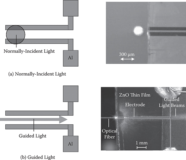
FIGURE 9.20 Setups of photocurrent measurements in (a) the normally incident light configuration and (b) the guided light configuration. From T. Yoshimura, A. Oshima, D. Kim, and Y. Morita, “Quantum dot formation in polymer wires by three-molecule molecular layer deposition (MLD) and applications to electro-optic/photovoltaic devices,” ECS Transactions 25, No. 4 “Atomic Layer Deposition Applications 5,” 15–25 (2009).
Note that in ZnO/CV, only small photocurrents are generated at 633 nm in spite of the fact that it has large light absorption at 633 nm. As mentioned in Section 9.1.3.1, electron injection efficiency from an n-type dye molecule like CV to ZnO is low, so only small photocurrents are generated. By inserting RB, which is a p-type dye molecule, between CV and ZnO, the electrons can be injected from CV to ZnO through RB with high efficiency.
As described above, in the structure of ZnO/RB/CV fabricated by liquid-phase MLD, widening of the photocurrent spectra was observed, providing the proof of concept for multidye sensitization shown in Figure 9.2(b). To extend the sensitized wavelength regions, longer molecular wires with more than three kinds of dye molecules should be formed on ZnO thin films by increasing the MLD step counts. The experimental trial is underway.
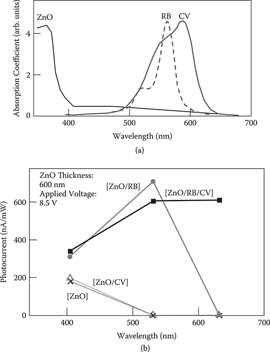
FIGURE 9.21 (a) Absorption spectra of ZnO, RB and CV, and (b) wavelength dependence of photocurrents measured by the guided light configuration in ZnO, ZnO/RB, ZnO/CV, and ZnO/RB/CV.
9.1.4 PROOF OF CONCEPT OF POLYMER-MQD SENSITIZATION
As mentioned in Section 4.2.2, by controlling molecular arrangements in conjugated poly-AM wires with designated sequences of three kinds of molecules using MLD, polymer wires with MQDs can be fabricated [4]. Figure 9.22 shows an example of a poly-AM-based polymer MQD by MLD with terephthalaldehyde (TPA), p-phenylenediamine (PPDA), and oxalic dihydrazide (ODH). Quantum dots of OT, OTPT, and OTPTPT are formed in a polymer wire to provide quantum dots with different lengths. The structure can be used for the polymer-MQD sensitization shown in Figure 9.2(c) [3,4].

FIGURE 9.22 An example of poly-AM-based polymer MQD by MLD with TPA, PPDA, and ODH.
In order to clarify the feasibility of the polymer MQD as a sensitizer for ZnO thin films, we examined the sensitizing ability of poly-AM wires as a preliminary trial.
In poly-AM, since the absorption band is located in wavelength regions of 350–500 nm as Figure 9.23(a) shows, sensitization in the blue-green regions is expected. Figure 9.23(b) shows wavelength dependence of photocurrents measured by the guided light configuration in ZnO and ZnO/poly-AM, which is a ZnO thin film with poly-AM grown on the surface by the carrier gas–type MLD. In ZnO/poly-AM, the photocurrents at 405 nm are enhanced, and the photocurrent spectrum extends to 532 nm, indicating that poly-AM wires have sensitizing ability in the blue-green regions.
It is preferable to grow poly-AM wires vertically from the ZnO surface to construct the polymer MQD structures shown in Figure 9.2(c). However, the sensitization effect is available even when the poly-AM wires are grown horizontally on the ZnO surface, as shown on the right-hand illustration of Figure 9.1(b). The control of the wire orientation can be done by SAM or other surface treatment [21, 22 and 23].
9.1.5 PROOF OF CONCEPT OF WAVEGUIDE-TYPE PHOTOVOLTAIC DEVICES
As a measure of the photocurrent enhancement induced by the guided light configuration, photocurrent enhancement ratio (PCER) is defined as follows.
As Figure 9.24 shows, large PCERs of ~5, ~15, and ~8 are observed in ZnO at 405 nm, in ZnO/RB at 532 nm, and in ZnO/RB/CV at 633 nm, demonstrating the possibility of waveguide-type photovoltaic devices.
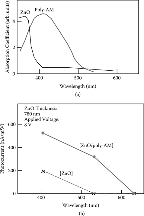
FIGURE 9.23 (a) Absorption spectra of ZnO and poly-AM, and (b) wavelength dependence of photocurrents measured by the guided light configuration in ZnO and ZnO/poly-AM.
Figure 9.25 shows wavelength dependence of the photocurrents in ZnO/poly-AM. Here, GL and NIL, respectively, represent the guided light configuration and the normally incident light configuration. PCERs of ~3 and ~12 are observed at 405 nm and at 532 nm, respectively. PCER is larger at 532 nm, where the light absorption of poly-AM is small, than PCER at 405 nm, where the light absorption of poly-AM is relatively large. It is found from the result that the photocurrent enhancement in the guided light configuration is more remarkable in wavelength regions with smaller light absorption. This is because in a wavelength region where the thin films have large light absorption, the thin films can absorb light to some extent even in the normally incident light configuration to generate photocurrents, and consequently, the PCER is reduced.
Thus, it is clarified that guided light beams can greatly enhance light absorption efficiency. This suggests that waveguide-type photovoltaic devices are promising to improve the efficiency of sensitized photovoltaic devices with flat-surface thin-film semiconductors. As future work, practical waveguide-type photovoltaic devices with multidye sensitization and polymer-MQD sensitization will be fabricated.
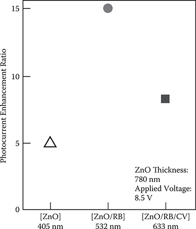
FIGURE 9.24 Photocurrent enhancement in ZnO, ZnO/RB, and ZnO/RB/CV.
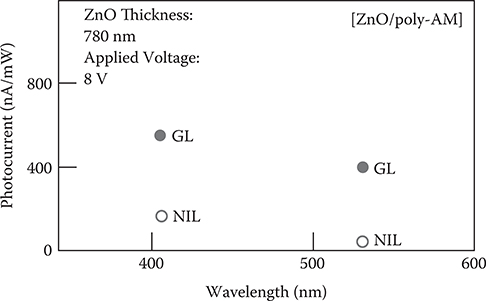
FIGURE 9.25 Wavelength dependence of the photocurrents in ZnO/poly-AM for the guided light configuration (GL) and the normally incident light configuration (NIL).
In waveguide-type photovoltaic devices, the optical coupling method for introducing light beams into the optical waveguides of the photovoltaic device is an important issue, which is discussed in Section 9.1.2.
9.2 Integrated Solar Energy Conversion Systems
The integrated film systems shown in Figure 9.26 will provide various types of ubiquitous functions [1], including solar energy conversion films, wearable computers, system glasses, thin-film speakers, and so on. The integrated film systems whose structures are similar to those of optical interconnects within boxes, are one of the important applications of thin-film photonic devices.
In the present section, concepts of film-based integrated solar energy conversion systems and related devices such as the integrated photonic/electronic/chemical system (IPECS) and light beam collecting films are proposed [1,2,24, 25, 26 and 27].
9.2.1 CONCEPT OF INTEGRATED SOLAR ENERGY CONVERSION SYSTEMS
Solar energy conversion systems have received much attention because of their ability to resolve the problems of the environment and serious energy shortages. In conventional energy conversion systems, semiconductors such as Si are placed all over the solar energy conversion modules, so it is foreseen that the cost of the systems will increase because of a shortage of semiconductor materials. In systems with Fresnel lens/mirror concentrators, semiconductor materials can be saved because solar beams are focused on small semiconductor cells. However, the system size becomes very large, and furthermore, they need solar-beam tracking mechanisms to keep the focusing point of the solar beams on the small-sized semiconductor cells.
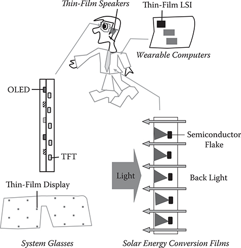
FIGURE 9.26 Integrated film systems.
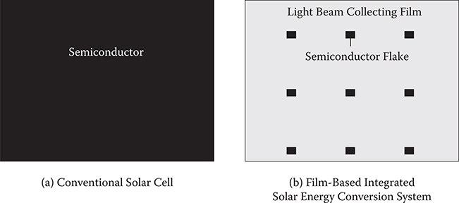
FIGURE 9.27 Concept of (a) the conventional solar cell and (b) the film-based integrated solar energy conversion system. From R. Shioya and T. Yoshimura, “Design of solar beam collectors consisting of multi-layer optical waveguide films for integrated solar energy conversion systems” Journal of Renewable and Sustainable Energy 1, 033106-1-15 (2009).
To reduce the consumption of semiconductor materials, to provide wide-angle light beam collecting capability to these systems, and to make the systems flexible and compact, we proposed film-based integrated solar energy conversion systems with optical waveguides [1,2,24–27].
Figure 9.27 shows schematic illustrations of the conventional solar cell and the film-based integrated solar energy conversion system using optical waveguides for light beam collecting. In integrated solar energy conversion systems, semiconductor flakes are placed partially in a light beam collecting film by a heterogeneous integration process such as PL-Pack with SORT described in Section 7.5. In some cases, the semiconductor flakes are placed outside of the film with solar beams guided by optical fibers.
The advantages and possible applications of the film-based integrated solar energy conversion systems are summarized in Table 9.2. The proposed structures can reduce semiconductor material consumption. This enables us to use expensive III-V compound semiconductors, which have higher photovoltaic conversion efficiency than Si. Conversion efficiency could be improved by delivering collected light beams of different wavelength regions to semiconductors having matched sensitivity spectra using wavelength filters in the optical circuits of the light beam collecting films. Since the integrated solar energy conversion system has waveguide structures, the waveguide-type photovoltaic devices described in Section 9.1 are easily integrated into the system.
9.2.2 THE INTEGRATED PHOTONIC/ELECTRONIC/CHEMICAL SYSTEM (IPECS)
A schematic model of IPECS is shown in Figure 9.28(a) [1,2,24, 25 and 26]. IPECS has a structure similar to the integrated optical interconnects shown in Figure 9.28(b), and is built by following core technologies: 3-D optical circuits for constructing the backbone of light beam collecting films, PL-Pack with SORT for embedding thin-film photovoltaic devices, SOLNET for self-aligned optical couplings between optical waveguides and thin-film photovoltaic devices, and MLD for high-performance thin-film photovoltaic devices. In some cases, IPECS contains fluidic circuits for supplying electrolytes to the system.
TABLE 9.2
Advantages and Possible Applications of Film-Based Integrated Solar Energy Conversion Systems
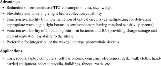
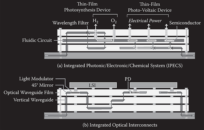
FIGURE 9.28 (a) Integrated photonic/electronic/chemical system (IPECS) and (b) integrated optical interconnects. From T. Yoshimura, “Proposed Applications of 3-D optical interconnect technologies to integrated chemical systems,” Digest of the LEOS Summer Topical Meetings (Bio-Inspired Sensors and Application/Imprinting on Photonic Integrated Circuits), Portland, Oregon, 129–130 (2007).
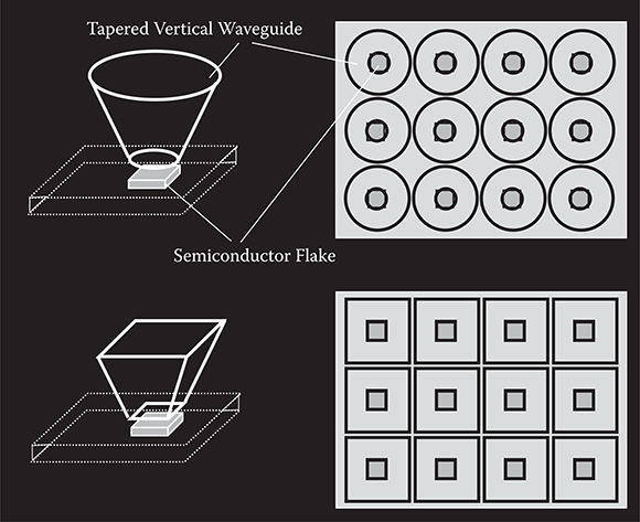
FIGURE 9.29 Integrated solar energy conversion system with a tapered vertical waveguide-type light beam collecting film.
9.2.3 STRUCTURES OF LIGHT BEAM COLLECTING FILMS
We proposed three types of light beam collecting films: The tapered vertical waveguide type, the tapered vertical/horizontal waveguide type, and the multilayer waveguide type.
Figure 9.29 shows an example of the integrated solar energy conversion system with a tapered vertical waveguide-type light beam collecting film. Thin-film photovoltaic devices or photosynthesis devices containing semiconductor flakes are embedded in the film. The incident light beams received by the tapered vertical waveguides are guided to the semiconductor flakes, whose areas are smaller than the areas of the light beam collecting aperture of the vertical waveguide. This enables a reduction of semiconductor consumption, that is, cost for solar energy conversion. In this example, the material consumption can be reduced to ~1/9 of the consumption in conventional solar cells.
Figure 9.30 shows an example of the system with a tapered vertical/horizontal waveguide-type light beam collecting film. A film with tapered vertical waveguides and a film with horizontal waveguides having vertical mirrors are stacked. The incident light beams are introduced into the horizontal waveguides through the vertical mirrors and guided to embedded semiconductor flakes. This enables further reduction of semiconductor consumption. In this example, the material consumption can be reduced to ~(1/9) × (1/16) = ~1/144 of the consumption in conventional solar cells. By embedding wavelength filters into the waveguide films, solar beams can branch to semiconductors having matched spectral responses. For example, UV-blue beams to ZnO, visible beams to Si, and infrared beams to InP.
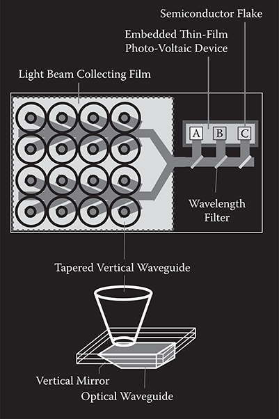
FIGURE 9.30 Integrated solar energy conversion system with a tapered vertical/horizontal waveguide-type light beam collecting film. From T. Yoshimura, “Proposed Applications of 3-D optical interconnect technologies to integrated chemical systems,” Digest of the LEOS Summer Topical Meetings (Bio-Inspired Sensors and Application/Imprinting on Photonic Integrated Circuits), 129–130 (2007).
Figure 9.31 shows an example of the system with a multilayer waveguide-type light beam collecting film. Many films with horizontal waveguides having vertical mirrors are stacked. The incident light beams are introduced through the vertical mirrors into the horizontal waveguides and are guided to semiconductor flakes.
An example of the integration of a waveguide-type photovoltaic device and a light beam collecting film is shown in Figure 9.32. The incident light beams received by the tapered vertical waveguides are guided to the bottom, where cone-shaped 45° mirrors are placed. The light beams are introduced into waveguide-type photovoltaic devices through the 45° mirrors.
Figure 9.33 shows an example of coloring of the integrated solar energy conversion systems by back lights. In conventional solar cells, since semiconductors are placed on the whole substrate, the cells look black. To avoid the monochromatic characteristics of solar cells, in some dye-sensitized solar cells, colored appearance is available by suppressing light absorption in some wavelength regions. This causes reduction of energy conversion efficiency. In integrated solar energy conversion systems, back light can pass through the light beam collecting film. By adjusting the color of the back lighting, specific coloration of the film may be achievable, which improves the appearance of solar cells.

FIGURE 9.31 Integrated solar energy conversion system with a multilayer waveguide-type light beam collecting film.
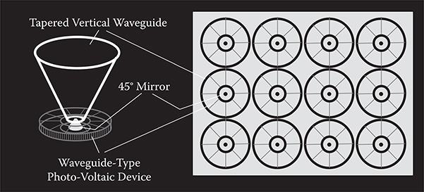
FIGURE 9.32 An example of integration of a waveguide-type photovoltaic device and a light beam collecting film.
9.2.4 DESIGN OF LIGHT BEAM COLLECTING FILMS
In the present subsection, the results of the design of the light beam collecting films and estimation of their light beam collecting ability by the beam propagation method (BPM) and the finite difference time domain (FDTD) method are presented [27].
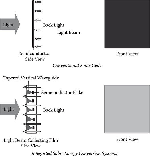
FIGURE 9.33 Coloring of the integrated solar energy conversion systems by back lights.
The tapered vertical waveguide-type light beam collecting film and the tapered vertical/horizontal waveguide-type light beam collecting film are basically regarded as similar structures except for the merging waveguides. So the simulation was carried out for the tapered vertical/horizontal waveguide-type light beam collecting film and the multilayer waveguide-type light beam collecting film.
9.2.4.1 Simulation Procedure
An example of a simulation model for light beam collection in the waveguide-type light beam collecting film is shown in Figure 9.34. An incident light beam from a metal mirror is introduced into a horizontal waveguide via a tapered vertical waveguide and a vertical mirror. The refractive index of the optical waveguides is 1.6, and the refractive index of the background is 1.0, assuming air. The width of the horizontal waveguide is 4 µm. An antireflective (AR) coating with a 100-nm thickness and a refractive index of 1.3 is applied to the top and the bottom of the optical waveguide. An incident light beam with a large width is preferable to reproduce the condition of plane waves of sunlight. However, when the width is broadened, the area of the FDTD calculation must be large, making computation time extremely long. So in the present work, the simulations were performed using a fundamental guided beam in an optical waveguide with a width of 10 µm for the incident light beam. Incident angles of the light beam are adjusted by the metal mirror. Wavelengths of the incident light beams are 400, 600, and 800 nm. The length of the model from the left boundary to the right boundary is 200 µm. Light intensity at the output (the right boundary of the model) is calculated to estimate the light beam collecting efficiency for various models.
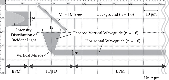
FIGURE 9.34 An example of a simulation model for light beam collection in waveguide-type light beam collecting films.
9.2.4.2 Tapered Vertical/Horizontal Waveguide-Type Light Beam Collecting Films
In Figure 9.35, models and the light intensity for light beam propagation in waveguide-type light beam collecting films are shown. Figure 9.35(a) shows a model without the tapered vertical waveguide. Considerable leakage is observed at the vertical mirror. The light beam collecting efficiency was 61%.
Figures 9.35(b) and (c) show models of tapered vertical/horizontal waveguide-type light beam collecting films with a tapered vertical waveguide having a high-refractive-index upper part (Model UH) and a high-refractive-index lower part (Model LH), respectively. The tapered angle of the tapered vertical waveguide is λT = 17°.
While the light beam collecting efficiency was 61% in Model UH, the efficiency increased up to 77% in Model LH. This can be explained as follows. Since the light beam spot size becomes small with propagation of the light beams to the lower region of the tapered vertical waveguide, stronger light beam confinement is necessary in the lower region. By putting the high-refractive-index material in the lower regions, strong light beam confinement can be effectively achieved, resulting in an increase in the light beam collecting efficiency.
In order to increase the collecting efficiency further, the tapered angles and refractive index distribution profiles in the tapered vertical waveguides should be optimized.
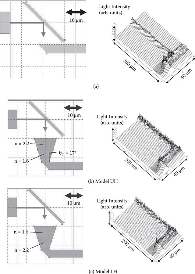
FIGURE 9.35 Models and the propagating light intensity for tapered vertical/horizontal waveguide-type light beam collecting films. (a) Without the tapered vertical waveguide, (b) with a tapered vertical waveguide having high-refractive-index upper part (Model UH), and (c) with a tapered vertical waveguide having high-refractive-index lower part (Model LH).
9.2.4.3 Multilayer Waveguide-Type Light Beam Collecting Films
A model for the multilayer waveguide-type light beam collecting film is shown in Figure 9.36. The model consists of stacked waveguide films. In this example, as shown in the side view, 18 optical waveguide films are stacked. Numbers in the top view indicate vertical mirror apertures, that is, the light beam collecting apertures, of a film denoted by the numbers. An example of optical circuits in a film is illustrated in Figure 9.37. Merging waveguides for light beam collection from the vertical mirrors through the branching waveguides to the main waveguide are integrated. By arranging the films regularly with one-aperture displacement, the surface can be occupied by the light beam collecting apertures in high density, achieving aperture occupation of 100%, theoretically.
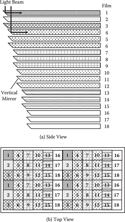
FIGURE 9.36 Model for the multilayer waveguide-type light beam collecting film. From R. Shioya and T. Yoshimura, “Design of solar beam collectors consisting of multi-layer optical waveguide films for integrated solar energy conversion systems” Journal of Renewable and Sustainable Energy 1, 033106-1-15 (2009).
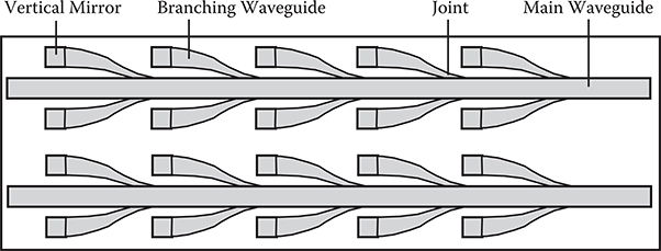
FIGURE 9.37 An example of optical circuits of merging waveguides.
9.2.4.3.1 Effects of Incident Angles on Collecting Efficiency for Single-Layer Optical Waveguide Films
Figure 9.38 shows models with 45° mirrors and the propagating light intensity for incident angles of 0o, 45°, and −45°. The wavelength of incident light beams is 600 nm. Here, in the model of −45°, the waveguide direction is flipped horizontally, which effectively reproduces a configuration for −45° incidence with the same incident light beam direction as for the 45° incidence. For an incident angle of 0°, a light beam is introduced into the optical waveguide through the 45° mirror, and then guided in the optical waveguide smoothly, indicating that the fundamental mode is dominant. For incident angles of 45° and −45° a lot of leakage of light beams passing through the 45° mirror are observed. At the same time considerable higher modes are excited in the guided beams.
Figure 9.39 shows models with 30° mirrors and the propagating light intensity for incident angles of 0° and 45°. For an incident angle of 0°, a light beam guided in the optical waveguide contains considerable higher modes. For an incident angle of 45°, on the other hand, the guided beam propagates smoothly with a small amount of higher modes. Figure 9.40 shows models with 60° mirrors and the propagating light intensity for incident angles of 0° and 45°. The guided beam contains a lot of higher modes for both incident angles.
The light beam collecting efficiency is summarized in Figure 9.41. For an incident angle of 0°, the 45° mirror exhibits the largest efficiency of 62%, and for an incident angle of 45°, the 30° mirror exhibits the largest efficiency of 47%. The 60° mirror does not exhibit great efficiency for incident angles of 45° and 0o. From these results, it is concluded that optical waveguides with 45° mirrors and those with 30° mirrors are respectively useful for the incident light beam with a vertical direction and for that with a tilted direction.
9.2.4.3.2 Effects of Layer Counts on Collecting Efficiency
Figure 9.42 shows a model of a three-layer waveguide structure with 45° mirrors and the propagating light intensity for an incident light beam with a wavelength of 600 nm. The distance between optical waveguides is 1 µm. It is found that the incident light beam, which goes through the first layer, is received by the second layer and the third layer to increase the light beam collecting efficiency. As Table 9.3 shows, light beam collecting efficiency increases from 62% to 87% with increasing the layer counts from one to three.
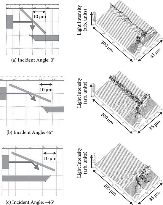
FIGURE 9.38 Models with 45° mirrors and propagating light intensity for incident angles of (a) 0°, (b) 45°, and (c) −45°. From R. Shioya and T. Yoshimura, “Design of solar beam collectors consisting of multi-layer optical waveguide films for integrated solar energy conversion systems” Journal of Renewable and Sustainable Energy 1, 033106-1-15 (2009).
9.2.4.3.3 Collecting Efficiency in Multi-Layer Waveguides with 45° and 30° Mirrors
A schematic structure of a light beam collecting film consisting of multilayer optical waveguides with 45° and 30° mirrors is illustrated in Figure 9.43. The first layer is an optical waveguide with a 45° mirror, and the second and third layers are optical waveguides with a 30° mirror. The two optical waveguides with 30° mirrors are arranged in opposite directions. The first layer is for incident light beams with vertical directions. The second layer is for beams from the left side direction, and the third layer is for beams from the right side direction. This structure is expected to provide wide-angle light beam collecting capability without solar beam tracking mechanisms.
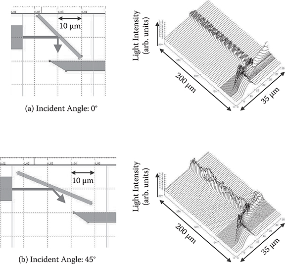
FIGURE 9.39 Models with 30° mirrors and propagating light intensity for incident angles of (a) 0° and (b) 45°. From R. Shioya and T. Yoshimura, “Design of solar beam collectors consisting of multi-layer optical waveguide films for integrated solar energy conversion systems” Journal of Renewable and Sustainable Energy 1, 033106-1-15 (2009).
Figure 9.44 shows models of the three-layer structure and the propagating light intensity. The wavelength of the incident light beams is 600 nm. It is found that the light beam is mainly collected by the first layer for vertical incidence, by the second layer for tilted incidence from the left, and by the third layer for tilted incidence from the right.
For comparison, the light beam collecting characteristics of a light beam collecting film consisting of a three-layer structure with only 45° mirrors are examined. The structure is shown in Figure 9.45. It is the same as the model shown in Figure 9.44 except for the mirror angles. While the collected light beam propagates in the optical waveguides smoothly for vertical incidence, for tilted incidence the collected light beam is reduced and propagates in considerably higher modes.
Figure 9.46 shows dependencies of light beam collecting efficiency on incident angles for the three-layer structure having optical waveguides with 45° and 30° mirrors (denoted by 45°/30°/30°) and the structure having optical waveguides with only 45° mirrors (denoted by 45°/45°/45°). The 45°/30°/30° version exhibits higher efficiency than 45°/45°/45°. Especially for an incident angle of 45°, the efficiency is 1.5 times larger in 45°/30°/30° than in 45°/45°/45°. This indicates that the light beam collecting film consisting of multilayer optical waveguides with mirrors of different angles provides wide-angle light beam collecting capability.
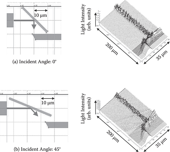
FIGURE 9.40 Models with 60° mirrors and propagating light intensity for incident angles of (a) 0° and (b) 45°. R. Shioya and T. Yoshimura, “Design of solar beam collectors consisting of multi-layer optical waveguide films for integrated solar energy conversion systems” Journal of Renewable and Sustainable Energy 1, 033106-1-15 (2009).
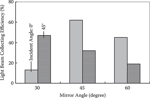
FIGURE 9.41 Light beam collecting efficiency in models with 30°, 45°, and 60° mirrors for incident angles of 0° and 45°. From R. Shioya and T. Yoshimura, “Design of solar beam collectors consisting of multi-layer optical waveguide films for integrated solar energy conversion systems” Journal of Renewable and Sustainable Energy 1, 033106-1-15 (2009).
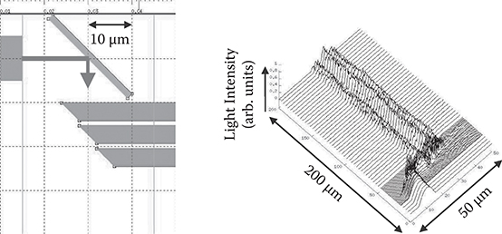
FIGURE 9.42 Model of a three-layer waveguide structure with 45° mirrors and propagating light intensity. From R. Shioya and T. Yoshimura, “Design of solar beam collectors consisting of multi-layer optical waveguide films for integrated solar energy conversion systems” Journal of Renewable and Sustainable Energy 1, 033106-1-15 (2009).
TABLE 9.3
Light Beam Collecting Efficiency for Layer Counts of One, Two, and Three
layer count |
light beam collecting efficiency (%) |
1 |
62 |
2 |
83 |
3 |
87 |
It should be noted that the model shown in Figure 9.44 has 4 µm × 4 µm aperture in top views. This corresponds to the aperture occupation for a layer count of one in Table 9.3. So, when a 3 × (4 µm × 4 µm) aperture, which corresponds to a layer count of three in Table 9.3, is built by stacking two more film units of 45°/30°/30°, light beam collecting efficiency of more than 80% might be expected for incident angles of 45° and 0°.
The light beam collecting efficiency for an incident angle of 45° were calculated to be 60% and 65% for wavelengths of 400 and 800 nm, respectively. Thus, it is found that the wavelength dependence of the efficiency is relatively small, indicating that the proposed model could operate in wavelength regions from 400 nm to 800 nm.
9.2.4.3.4 Overall Consideration
Overall light beam collecting efficiency ηOver All is given as follows:
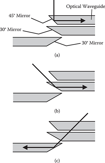
FIGURE 9.43 Schematic structure of a light beam collecting film consisting of multilayer optical waveguides with 45° and 30° mirrors. (a) Incident light beams with vertical directions, (b) incident light beams from the left side directions, and (c) incident light beams from the right side directions. From R. Shioya and T. Yoshimura, “Design of solar beam collectors consisting of multi-layer optical waveguide films for integrated solar energy conversion systems” Journal of Renewable and Sustainable Energy 1, 033106-1-15 (2009).
Here, ηMirror, ηMerging, and ηSemiconductor are, respectively, the light beam collecting efficiency via a vertical mirror, the light beam propagation efficiency via merging waveguides, and the coupling efficiency between an optical waveguide and a semiconductor flake.
As mentioned in Sections 9.2.4.3.2 and 9.2.4.3.3, η Mirror of the tapered vertical/horizontal waveguide-type light beam collecting film (Model LH) and η Mirror of the multilayer waveguide-type light beam collecting film (three-layer structure of 45°/30°/30°) are expected to be around 80%. For ηSemiconductor, when ZnO (refractive index n: 2.1) is used for the semiconductor and polymers (n: 1.52) for optical waveguides, reflection loss at the interfaces is ~16%. The coupling efficiency may increase to ~100% by inserting an appropriate AR coating.
ηMerging was calculated by BPM. The model is similar to that shown in Figure 9.37. The branching angle is 10°. The branching waveguides are tapered from a width of 4 µm at the vertical mirror to 0.1 µm at the joint, which is effective to increase the light beam propagation efficiency. Figure 9.47(a) shows the dependence of total propagation efficiency on the number of joints when light beams are introduced into all the vertical mirrors. The efficiency decreases with increases in the number of joints. For a joint count of 8, the efficiency is 52%.

FIGURE 9.44 Models of the three-layer structure with 45° and 30° mirrors and propagating light intensity for incident angles of (a) 0°, (b) 45°, and (c) −45°. From R. Shioya and T. Yoshimura, “Design of solar beam collectors consisting of multi-layer optical waveguide films for integrated solar energy conversion systems” Journal of Renewable and Sustainable Energy 1, 033106-1-15 (2009).
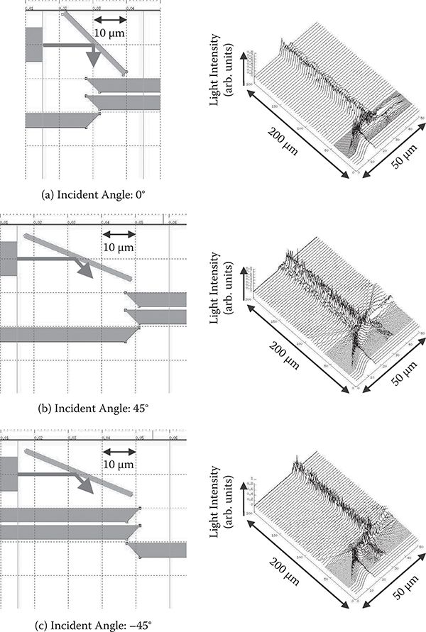
FIGURE 9.45 Models of the three-layer structure with only 45° mirrors and propagating light intensity for incident angles of (a) 0°, (b) 45°, and (c) −45°. From R. Shioya and T. Yoshimura, “Design of solar beam collectors consisting of multi-layer optical waveguide films for integrated solar energy conversion systems” Journal of Renewable and Sustainable Energy 1, 033106-1-15 (2009).
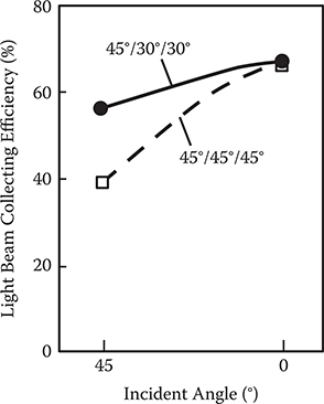
FIGURE 9.46 Dependence of light beam collecting efficiency on incident angles for 45°/30°/30° and 45°/45°/45°. From R. Shioya and T. Yoshimura, “Design of solar beam collectors consisting of multi-layer optical waveguide films for integrated solar energy conversion systems” Journal of Renewable and Sustainable Energy 1, 033106-1-15 (2009).
By substituting η Mirror~80%, ηMerging~50%, and ηSemiconductor~100% into Equation (9.3), the expected overall light beam collecting efficiency is calculated to be ~40% for the joint count of 8.
In the case of the eight-step merging, light beams from 16 vertical mirrors are collected into one semiconductor flake. Therefore, the semiconductor consumption reduction factor, denoted by FSCR, is 1/16 in an integrated solar energy conversion system with the multilayer waveguide-type light beam collecting film. For the systems with the tapered vertical/horizontal waveguide-type light beam collecting film, as discussed in Section 9.2.3, semiconductor consumption reduction of 1/9 is obtained at the tapered waveguide part. Therefore, the eight-step merging gives us FSCR of (1/9) × (1/16) = 1/144. In the conventional solar cell, FSCR is 1 because the semiconductor is placed over the entire module.
As a measure of resource-saving ability, a ratio of ηOver All /FSCR is defined. This ratio is proportional to the amount of energy conversion achieved by semiconductors of unit volume. In the conventional solar cell, since ηOver All is nearly equal to 100%, ηOver All /FSCR ratio is 100/1 = 100. For integrated solar energy conversion systems with multilayer waveguide-type light beam collecting film, influence of the number of joints in the merging waveguides on the ηOver All /FSCR ratio is shown in Figure 9.47(b). The ratio increases with the joint counts, followed by saturation. In the case of eight-step merging, the ratio is 40/(1/16) = 640, which is 6.4 times larger than the ratio in the conventional solar cell. For the systems with the tapered vertical/horizontal waveguide-type light beam collecting film, the ηOver All /FSCR ratio might be 40/(1/144) = 5760, which is 58 times larger than the ratio in the conventional solar cell. Thus, it is concluded that the proposed integrated solar energy conversion systems are expected to realize savings in materials.

FIGURE 9.47 Dependence of (a) total propagation efficiency and (b) ratio of ηOver All /FSCR on the number of joints in the merging waveguides.
In the multilayer waveguide-type light beam collecting film, in order to achieve aperture occupation of 100%, 39 layers are necessary for one angle of the vertical mirrors when the branching angle and the joint counts are, respectively, 10° and 8 in the merging waveguide. This 39-layer structure forms one module unit. To construct a multilayer structure consisting of optical waveguides with 45° and 30° mirrors, one module unit for 45° mirrors and four module units for 30° mirrors are necessary to be stacked in order to collect light beams with vertical incident angles and tilted incident angles (from the left side, right side, front side, and back side). When the waveguide core thickness is 4 µm and the distance between waveguides is 1 µm, the module unit thickness is around 195 µm. Then, total thickness of the stack of five module units is 975 µm.
The estimated efficiency of the waveguide-type light beam collecting films is lower than that of Fresnel lens/mirror concentrators. So, at present, the light beam collecting films do not seem to be suitable for large-scale solar energy conversion centers. However, they have an outstanding feature of flexible light-weight films, enabling us to carry them as sheets everywhere and put them on cars, robots, buildings, roofs of fragile houses, surfaces of pavements/roads, walls, tables, various kinds of equipment, clothes, and everywhere we want. They also have a unique feature of color appearance as illustrated in Figure 9.33. Since very high efficiency is not always necessary in these applications, light beam collecting film may still be useful.
9.2.5 POSSIBLE FABRICATION PROCESS
The built-in mask method and PL-Pack with SORT respectively described in Sections 7.6 and 7.5 can be applied to fabrication of light beam collecting films. For the tapered vertical waveguide-type light beam collecting film, a film with an array of tapered vertical waveguides is formed by tilted exposure using the built-in mask method. The film is stacked on a film, into which semiconductor flakes are embedded by PL-Pack with SORT. For the tapered vertical/horizontal waveguide-type light beam collecting film, a film with an array of tapered vertical waveguides is stacked on an optical waveguide film containing optical circuits of merging horizontal waveguides with embedded semiconductor flakes.
For the multilayer waveguide-type light beam collecting film, optical waveguide films containing optical circuits with merging horizontal waveguides are stacked on each other with sliding with one-vertical mirror-aperture displacement. The film separation can be kept by inserting spacers between films. With respect to light beam confinement, all-air-cladding waveguides are preferable. The all-air-cladding structures can be built by core transfers from one substrate to another substrate using PL-Pack with SORT, which enables us to place waveguide cores and spacers onto films at one time as demonstrated in Section 7.5.3. For waveguide fabrication, the built-in mask method as well as imprinting and stamping can be used.
9.2.6 IMPACT OF POLYMER MQDS ON INTEGRATED SOLAR ENERGY CONVERSION SYSTEMS
For the photovoltaic device embedded in the waveguide-type light beam collecting films, the waveguide-type photovoltaic device described in Section 9.1 is a promising candidate. The waveguide-type photovoltaic device with multidye sensitization and polymer-MQD sensitization achieved by MLD might be especially promising for future high-performance energy conversion systems.
9.3 Novel Structures of Photovoltaic and Photosynthesis Devices
In addition to the waveguide-type photo-voltaic devices described in Section 9.1, other kinds of novel photo-voltaic and photo-synthesis devices might be used in the integrated solar energy conversion systems. Figure 9.48 shows examples of a thin-film photo-voltaic device and a photo-synthesis device, which might be integrated in the light beam collecting films described in Section 9.2. In the thin-film photo-voltaic device, a collected light beam is introduced onto a semiconductor film through an optical waveguide with a vertical mirror. This structure enables us to replace an expensive and electrically resistive transparent electrode with a low-cost metal electrode with low resistivity.
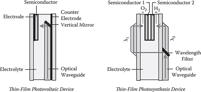
FIGURE 9.48 Examples of thin-film photovoltaic and photosynthesis devices. From T. Yoshimura, “Proposed applications of 3-D optical interconnect technologies to integrated chemical systems,” Digest of the LEOS Summer Topical Meetings (Bio-Inspired Sensors and Application/Imprinting on Photonic Integrated Circuits), Portland, Oregon, 129–130 (2007).

FIGURE 9.49 Positional configurations of thin films in thin-film photosynthesis devices.
In the thin-film photosynthesis device, using 3-D optical circuits with embedded wavelength filters, collected light beams branch into two optical paths for wavelengths of λ1 and λ2, which are respectively introduced onto two semiconductor thin films in an electrolyte, generating H2 and O2.
The photosynthesis process using two semiconductors is developed by Sayama et. al [28] using a solution in which semiconductor powders are dispersed. Since control of the relative positions of the two kinds of semiconductors is important for improving the photosynthesis performance, a thin-film structure approach shown in Figure 9.48, where the thin film locations are presicely controlled, seems promising. Figure 9.49 shows several examples for positional configurations of thin films in thin-film photosynthesis devices. For optimization of H+ diffusion in the solution, dividing the thin films or opening windows in the thin films might be effective.
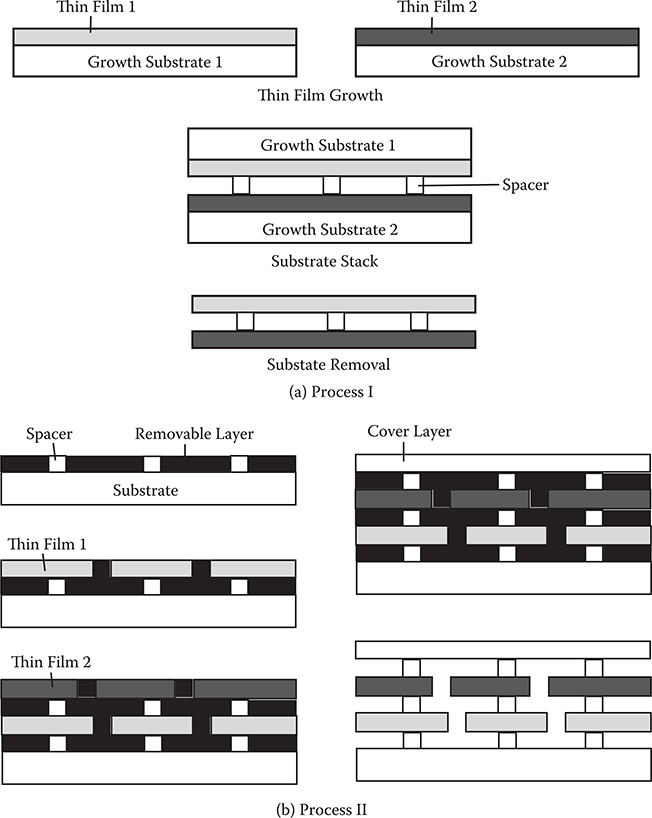
FIGURE 9.50 Possible fabrication processes for thin-film photosynthesis devices.
Possible fabrication processes for thin-film photosynthesis devices are shown in Figure 9.50. In process I, thin film 1 and thin film 2 are respectively grown on growth substrate 1 and growth substrate 2. The films are attached to each other with spacers between them. Then the growth substrates are removed to obtain stand-alone coupled thin films. In process II, thin film 1 is deposited on a removable layer of a substrate with spacers. Then, another removable layer and spacers are formed on thin film 1, and thin film 2 is deposited on them. After a cover layer is formed, all the removable layers are removed by etching to obtain a structure with thin films located in designated distributions three dimensionally.
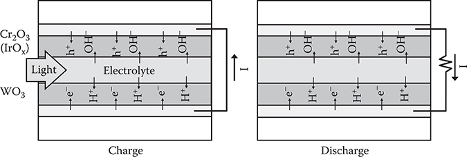
FIGURE 9.51 Waveguide-type photovoltaic device with a charge storage function.
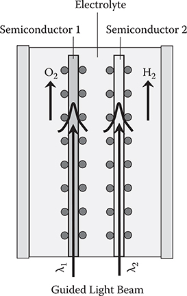
FIGURE 9.52 Waveguide-type dye-sensitized thin-film photosynthesis device.
9.4 Waveguide-Type Photovoltaic Devices With a Charge Storage/Photosynthesis Function
The waveguide-type photovoltaic device shown in Figure 9.51 has a charge storage function. Electrochomic WO3 thin film is an n-type semiconductor and exhibits a charge storage function as described in Section 2.6.1 as well as a coloration function. So, when a light beam is guided in a stack of WO3/electrolyte, it is expected that a charge is generated and stored in the WO3 thin film. In the model illustrated in Figure 9.51, a p-type semiconductor thin film (Cr2O3, IrxO, etc.) is placed on the counter electrode. This configuration is preferable to keep the system stable because electrons and protons are stored in WO3 and holes and anions are stored in the p-type semiconductor thin film.
An example of a waveguide-type dye-sensitized thin-film photosynthesis device is shown in Figure 9.52. Instead of normally incident light beams, guided light beams in the semiconductor thin films are used. The light beams pass through a lot of dye molecules, which enhances the light absorption in the thin-film semiconductors to generate gases efficiently.
References
1. T. Yoshimura, Molecular nano systems: Applications to optoelectronic computers and solar energy conversion, Corona Publishing Co., Ltd., Tokyo (2007) [in Japanese].
2. T. Yoshimura, Integrated photonic/electronic/chemical systems, solar energy conversion systems, light collectors, and optical waveguides” Japanese Patent Tokukai 2009-4717 (2009) [in Japanese].
3. T. Yoshimura and D. Kim, “A molecular-controlling deposition method and its applications to solar cells, electro-luminescent devices and optical switches” Japanese Patent Tokugan 2009-102408 [in Japanese].
4. T. Yoshimura, A. Oshima, D. Kim, and Y. Morita, “Quantum dot formation in polymer wires by three-molecule molecular layer deposition (MLD) and applications to electro-optic/photovoltaic devices,” ECS Transactions 25, No. 4 “Atomic Layer Deposition Applications 5,” from the 216th ECS Meeting, Vienna, Austria, 15–25 (2009).
5. T. Yoshimura, “Molecular layer deposition and applications to solar cells and the cancer photodynamic therapy,” Japanese Patent, Tokugan 2010-206098 (2010) [in Japanese].
6. C. Brauchle, U. P. Wild, D. M. Burland, G. C. Bjorkund, and D. C. Alvares, “Two-photon holographic recording with continuous-wave lasers in the 750-1100-nm range,” Opt. Lett. 7, 177–179 (1982).
7. V. D. McGinniss and R. E. Schwerzel, “Photopolymerizable composition containing a photosensitive donor and photoinitiating acceptor,” US Patent 4,571,377 (1986).
8. B. O’Regan and M. Gratzel, “ A low-cost high-efficiency solar cell based on dye-sensitized colloidal TiO2 films,” Nature 353, 737–740 (1991).
9. H. Shin and C. Bae, “Nanoscale tubular structures and ampoules of oxides,” AVS, 8th International Conference on Atomic Layer Deposition, TueM2-1, Bruges, Belgium (2008).
10. T. Yoshimura, S. Tatsuura, and W. Sotoyama, “Polymer films formed with monolayer growth steps by molecular layer deposition,” Appl. Phys. Lett. 59, 482–484 (1991).
11. T. Yoshimura, E. Yano, S. Tatsuura, and W. Sotoyama, Organic functional optical thin film, fabrication and use thereof, U.S. Patent 5,444,811 (1995).
12. T. Yoshimura, Liquid phase deposition, Japanese Patent, Tokukai Hei 3-60487 (1991) [in Japanese].
13. T. Yoshimura, Growth methods of polymer wires and thin films, Japanese Patent Tokukai 2008-216947 (2008) [in Japanese].
14. T. Yoshimura, K. Kiyota, H. Ueda, and M. Tanaka, “Contact potential difference of ZnO layer adsorbing p-type dye and n-type dye,” Jpn. J. Appl. Phys. 18, 2315–2316 (1979).
15. K. Kiyota, T. Yoshimura, and M. Tanaka, “Electrophotographic behavior of ZnO sensitized by two dyes,” Photogr. Sci. Eng. 25, 76–79 (1981).
16. T. Yoshimura, K. Kiyota, H. Ueda, and M. Tanaka, “Influence of illumination on the surface potential of ZnO adsorbing p-type dye and n-type dye,” Jpn. J. Appl. Phys. 19, 1007–1008 (1980).
17. T. Yoshimura, K. Kiyota, H. Ueda, and M. Tanaka, “Mechanism of spectral sensitization of ZnO coadsorbing p-type and n-type dyes,” Jpn. J. Appl. Phys. 20, 1671–1674 (1981).
18. H. J. Meier, “Sensitization of electrical effects in solids,” Phys. Chem. 69, 719–729 (1965).
19. H. Kokado, T. Nakayama, and E. Inoue, “A new model for spectral sensitization of photoconduction in zinc oxide powder,” J. Phys., & Chem. Solids 34, 1–8 (1973).
20. K. H. Hauffe, On spectral sensitization of Zinc oxide: Photogr. Sci. & Eng. 20, 124 (1976).
21. T. Yoshimura, S. Ito, T. Nakayama, and K. Matsumoto, “Orientation-controlled molecule-by-molecule polymer wire growth by the carrier-gas-type organic chemical vapor deposition and the molecular layer deposition,” Appl. Phys. Lett. 91, 033103-1-3 (2007).
22. T. Yoshimura and Y. Kudo, “Monomolecular-step polymer wire growth from seed core molecules by the carrier-gas type molecular layer deposition (MLD),” Appl. Phys. Express 2, 015502-1-3 (2009).
23. T. Yoshimura, K. Motoyoshi, S. Tatsuura, W. Sotoyama, A. Matsuura, and T. Hayano, “Selectively aligned polymer film growth on obliquely evaporated SiO2 pattern by chemical vapor deposition,” Jpn. J. Appl. Phys. 31, L980–L982 (1992).
24. T. Yoshimura, K. Ogushi, Y. Kitabayashi, K. Naito, Y. Miyamoto, and M. Miyazaki, “Optical waveguide films with two-layer skirt-type core end facets for beam leakage reduction at 45° mirrors,” Proc. SPIE 6899, from Photonics West 2008, San Jose, California, 689913- 1-11 (2008).
25. T. Yoshimura, “Proposed applications of 3-D optical interconnect technologies to integrated chemical systems,” Digest of the LEOS Summer Topical Meetings (Bio-Inspired Sensors and Application/Imprinting on Photonic Integrated Circuits), Portland, Oregon, 129–130 (2007).
26. T. Yoshimura and K. Asama, Integrated chemical systems and integrated light energy conversion systems, Japanese Patent Tokukai 2007-107085 (2007) [in Japanese].
27. R. Shioya and T. Yoshimura, “Design of solar beam collectors consisting of multi-layer optical waveguide films for integrated solar energy conversion systems” Journal of Renewable and Sustainable Energy 1, 033106-1-15 (2009).
28. K. Sayama and H. Arakawa, “Dream of Artificial Synthesis,” Newton. Newton Press, Tokyo, 102–109, September 2002 [in Japanese].