
7 Organic Photonic Materials, Devices, and Integration Processes
Although artificial thin-film organic materials fabricated by molecular layer deposition (MLD) and devices made of artificial materials are the final goal, sometimes, other kinds of thin-film organic materials and devices are still useful. Furthermore, in order to construct real optoelectronic (OE) systems, integration processes of the thin-film materials and devices are important.
In the present chapter, these materials and devices, and the integration processes are presented.
7.1 Electro-Optic (EO) Materials
Nonlinear optical devices such as EO devices, all-optical devices, and optical integrated circuits (ICs) consisting of these devices are key in optical communication, optical interconnects, and other OE systems. However, application areas of nonlinear optical devices are limited due to a lack of high-performance nonlinear optical materials.
Organic materials with π-conjugated systems have attracted interest as one of the candidates for nonlinear optical materials. The nonlinearity, as mentioned in Chapter 5, is predicted to be superior to that of conventional inorganic materials, such as LiNbO3 (LN) and the multiple quantum wells (MQWs) of compound semiconductors. Low dielectric constant characteristics are also an advantage of organic materials, especially for EO devices, enabling high speed and low power operation. Despite much work on organic materials, however, few notable improvements in optical nonlinearities have been made yet. It is important for the photonics world to make a breakthrough in the nonlinear optical properties of organic materials and to clarify the potential of the organic materials for EO devices.
The EO coefficients r of organic EO materials are compared in Figure 7.1. The materials can be classified into poled polymers [1], molecular crystals [2,3], and conjugated polymers [4,5]. The most promising EO material is the conjugated polymer [4,5]. As described in Chapter 5, polydiacetylene (PDA) wires with long π-conjugated systems are regarded as natural one-dimensional systems (quantum wires), and are more favorable to induce a larger oscillator strength than two- or three-dimensional systems. When multiple quantum dot (MQD) structures are introduced into the wires, the wires have long variable wavefunctions offering a greatly enhanced Pockels effect that is about 100 times r (LN). However, the conjugated EO polymers are a kind of far-reaching material. The second-best solutions are the molecular crystals and the poled polymers.
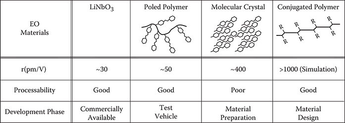
FIGURE 7.1 Organic nonlinear optical materials for EO devices.
For the molecular crystals, in 1987, using the AC modulation method, we found that the styrylpyridinium cyanine dye (SPCD) thin-film crystal exhibits an r of 430 pm/V, about 14 times that of LN [6]. This was the largest value ever observed in organic materials. The result demonstrated the prospect for applications of organic materials to EO devices. For the poled polymers, although r is usually smaller than that of the molecular crystals, they can be easily formed by spin-coating into thin films with high optical quality.
In the present section, various types of molecular crystals and poled polymers for EO materials are reviewed, and some examples of applications to polymer optical waveguides and optical switches are shown.
7.1.1 CHARACTERIZATION PROCEDURE FOR THE POCKELS EFFECT IN ORGANIC THIN FILMS
We developed the AC modulation method for characterization of the Pockels effect of organic thin films [6]. The schematic diagram of the experimental setup is shown in Figure 7.2(a). In order to apply an electric field to the thin films, a substrate, on which slit-type electrodes are formed, is pressed against the thin film. This method makes it possible to form electrodes on a small flake of organic thin film, say, with μm-order sizes. AC voltage from a function generator is applied between the electrodes. Linearly polarized light from a laser passes through the thin film and the electrode gap, and the light transmitted through the analyzer is detected by a photodetector.
In Figure 7.2(b) polarization states corresponding to positions I, II, and III, described in Figure 7.2(a), are schematically illustrated. The z and y components of the electric field of the laser (Ez and Ey) at positions I and II and the component along the analyzed polarization direction Eθ at position III can be written as follows:
Position I:

FIGURE 7.2 (a) Schematic diagram of experimental setup for the AC modulation method. (b) Polarization states corresponding to positions I, II, and III in (a). From T. Yoshimura, “Characterization of the EO effect in styrylpyridinium cyanine dye thin-film crystals by an ac modulation method,” J. Appl. Phys. 62, 2028–2032 (1987).
Position II:
Position III:
where φ is the angle between the polarization direction of incident light and the z-axis, θ is the angle between the analyzed polarization direction and the z-axis, and δ is the phase retardation arising from birefringence of the thin film. Then, the detector output Vout can be written as
δ varies depending on the voltage VA applied between the slit-type electrodes since the thin film has an EO effect. The detector output at VA = 0, denoted by Vdc, is given by
where δ0 is the phase retardation at VA = 0. When VA is increased from 0 to V, the phase retardation changes from δ0 to δ0 + Δδ. Δδ is the EO phase retardation induced by VA = V. Then the detector output change Vac is induced by applying VA = V and is given as follows.
From Equations (7.2) and (7.3),
is obtained. Substituting Equation (7.1) into Equation (7.4), an expression for Vac/Vdc related to the four parameters, that is, φ, θ, δ0, and Δδ is obtained. Here φ and θ are known, and δ0 is obtained from the angular dependence of Vdc. Therefore, by measuring Vac experimentally with the use of the setup illustrated in Figure 7.2(a), the EO phase retardation Δδ can be determined from Equation (7.4).
Once Δδ is obtained, the figure of merit of the EO phase retardation F is estimated according to the formula
where λ0 is the wavelength of the light in vacuum, D is the distance between the slit-type electrodes, and L is the film thickness.
The AC modulation method exhibits a high sensitivity for estimating EO effects since the lock-in technique is used. Therefore, the method is effective for characterizing thin-film EO materials.
7.1.2 MOLECULAR CRYSTALS
7.1.2.1 SPCD
A lot of studies have been done on second harmonic generation (SHG), which is one of the second-order nonlinear optical phenomena for molecular crystals. Some materials such as 2-methyl-4-nitroaniline (MNA) have been found to show extremely large SHG activity [2].
Molecular crystals have also been known to show the Pockels effect, which, as well as SHG, is involved in second-order nonlinearity. Lipscomb et al. studied the Pockels effect in an MNA single crystal and estimated the EO coefficient r11 to be 67 pm/V [3], which is about 2 times as large as r33 in LiNbO3.

FIGURE 7.3 Styrylpyridinium cyanine dye (SPCD). From T. Yoshimura, “Characterization of the EO effect in styrylpyridinium cyanine dye thin-film crystals by an ac modulation method,” J. Appl. Phys. 62, 2028–2032 (1987).
In the present subsection, first, the Pockels effect of SPCD molecular crystals is reported [6]. SPCD has a molecular structure schematically shown in Figure 7.3. Referring to an SHG measurement, SPCD shows extremely large SHG activity, about one order of magnitude larger than that in MNA [7]. Consequently, it is expected that in SPCD the Pockels effect would be several times larger than in MNA.
According to this guideline, we prepared SPCD thin film crystals and characterized the EO property of them. The characterization was performed by the AC modulation method described in Section 7.1.1. The accuracy of the method was confirmed by comparing the measured value with the value reported in other articles using LiNbO3 crystal as a standard sample.
7.1.2.1.1 Crystal Growth
An SPCD thin-film crystal was grown as follows. Two quartz substrates (55 × 55 × 1 mm3) were paired in a methanol solution of SPCD (Japanese Research Institute for Photosensitizing Dyes Co. Ltd.). The solution was inserted between the two substrates by capillary effect. After several days the methanol was evaporated naturally, and an SPCD thin film was grown between the substrates. The two substrates were separated carefully, and the thin film was left on one of the substrates. The film size typically ranges from 1–10 mm long, < 1 mm wide, and 3–10 μm thick. Observation of the SPCD thin film between crossed polarizers revealed that the SPCD thin film exhibits birefringence. When the thin film was rotated on a stage, some of the thin films showed complete and uniform extinction. These results indicate that the SPCD thin film is a single crystal. Since the SPCD crystal, as in most organic crystals, is not durable against mechanical, thermal, and chemical attack, we treated the crystal carefully during measurements.
7.1.2.1.2 Optical Properties
In Figure 7.4 a schematic shape of SPCD thin-film crystal is illustrated with a roughly estimated angle of each corner, as well as the absorption spectra of the crystal. Two optical axes are denoted by z and y. As can be seen in the figure, the light absorption of the SPCD thin-film crystal increases rapidly in the range above 2 eV, and the crystal shows strong dichroism. The absorption is greater for polarization along the z-axis than along the y-axis. This suggests that the molecular dipole moments of SPCD tend to align along the z-axis in the thin-film crystalline state.
Photoluminescence spectra of an SPCD thin-film crystal, SPCD powder used as the starting material for the crystal growth, and a water solution of SPCD were measured with a He-Cd laser (325 nm) excitation light source at room temperature. The luminescence spectrum of the SPCD powder appears in the low-energy side (peak position of 1.5 eV) compared with that of the SPCD thin-film crystal (peak position of 2.05 eV), and the luminescence intensity for the powder was about l/1000 of that for the crystal. This suggests that the electronic state in the crystal is largely different from the state in the powder. The spectrum of the SPCD crystal is relatively close to that of the water solution. This implies that in the crystal the electronic state of the SPCD molecule is like the state in water, that is, the interaction between SPCD molecules is weak.
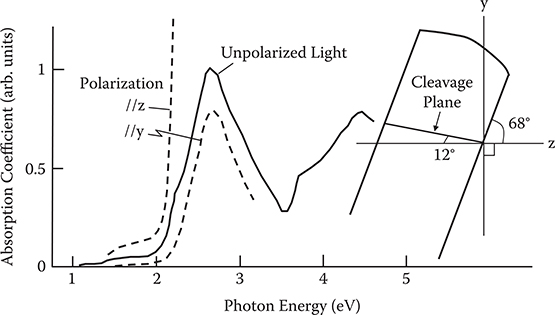
FIGURE 7.4 Schematic shape of SPCD thin-film crystal and its absorption spectra for polarized light. From T. Yoshimura, “Characterization of the EO effect in styrylpyridinium cyanine dye thin-film crystals by an ac modulation method,” J. Appl. Phys. 62, 2028–2032 (1987).
The refractive index of the SPCD thin-film crystal was estimated to be nz = 1.55 and ny = 1.31 by using the prism coupler method proposed by Wei and Westwood [8] and a differential interferometer. The result of nz > ny is consistent with the strong dichroism of the crystal and indicates again that the molecular dipole moments align along the z-axis.
7.1.2.1.3 Measurement
In order to apply an electric field to SPCD thin-film crystals, a substrate, on which slit-type NiCr electrodes (distance between the electrodes, 5 μm; electrode width, l00 μm; thickness 80 nm) are formed, was pressed against the thin-film crystal. Under application of AC voltage from a function generator between the electrodes, linearly polarized light at 633 nm from a He-Ne laser passed through the SPCD thin-film crystal and the electrode gap as shown in Figure 7.2. The light transmitted through the analyzer was detected by a solar cell.
7.1.2.1.4 Pockels Effect
As mentioned in Section 7.1.1, in order to estimate Δδ and F, Vdc and Vac must be measured. Vdc can be obtained straightforwardly by an oscilloscope. From the angular dependence of Vdc, δ0 is obtained. The result is shown in Figure 7.5 for a 5-μm-thick SPCD thin-film crystal. In Figure 7.6, a typical example of the light modulation introduced in the SPCD thin-film crystal by an 8-kHz sine wave is shown. Vac is superposed on Vdc. In this work for detecting Vac, the lock-in technique was used. Figure 7.7 shows Vac-versus-θ characteristics of the SPCD thin-film crystal for an electric field applied along the z-axis. Vac becomes zero at θ = 0°, 90°, and 180°, that is, in the direction of the optical axes (z-axis and y-axis), and has its maximum or minimum at θ = 45° and 135°. This behavior can be completely explained by Equations (7.3) and (7.1) and indicates that the rotation of the optical axes does not occur in the SPCD thin-film crystal when the electric field is applied along the z-axis. For comparison, Vac-versus-θ characteristics for a LiNbO3 crystal are also shown by a dotted line. The SPCD thin-film crystal exhibits Vac about 5 times larger than the LiNbO3 crystal. When the electric field was applied along the y-axis of the SPCD thin-film crystal, a maximum value of Vac was reduced to 1/3 of that with the electric field along the z-axis. This means that in the SPCD crystal, the EO effect is larger for the direction along the molecular dipole alignment than for the direction perpendicular to the dipole alignment.
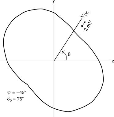
FIGURE 7.5 Vdc as a function of θ for a 5-μm-thick SPCD thin-film crystal. From T. Yoshimura, “Characterization of the EO effect in styrylpyridinium cyanine dye thin-film crystals by an ac modulation method,” J. Appl. Phys. 62, 2028–2032 (1987).
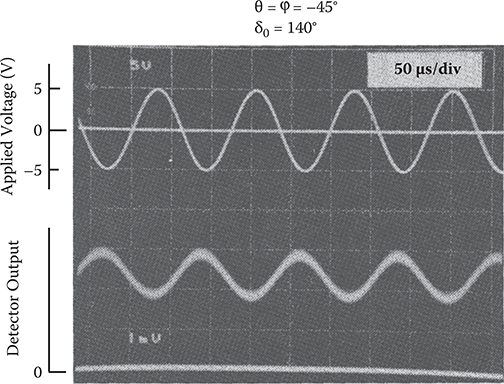
FIGURE 7.6 Light modulation introduced in the SPCD thin-film crystal by an 8-kHz sine wave. From T. Yoshimura, “Characterization of the EO effect in styrylpyridinium cyanine dye thin-film crystals by an ac modulation method,” J. Appl. Phys. 62, 2028–2032 (1987).
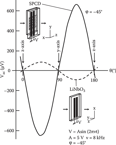
FIGURE 7.7 Vac as a function of θ for the SPCD thin-film crystal with electric field applied along the z-axis (solid line) and for a LiNbO3 crystal (dotted line). From T. Yoshimura, “Characterization of the EO effect in styrylpyridinium cyanine dye thin-film crystals by an ac modulation method,” J. Appl. Phys. 62, 2028–2032 (1987).
The EO phase retardation Δδ is obtained by substituting the experimental values, that is, φ = θ −45°, δ0 = 75°, Vdc = 14 mV, and Vac = 0.65 mV into Equations (7.1) and (7.4). The result is shown in Figure 7.8. The SPCD thin-film crystal shows Δδ = 7° at the applied voltage of 20 V, which corresponds to the half-wave voltage Vπ of 500 V, while the LiNbO3 crystal shows Δδ = 1.5° at 20 V, corresponding to Vπ = 2400 V.
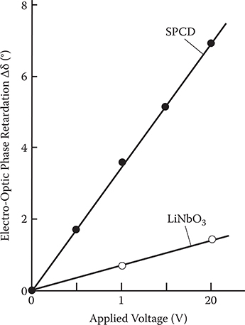
FIGURE 7.8 Dependence of EO phase retardation on applied voltage for the SPCD thin-film crystal with electric field applied along the z-axis (filled circles) and for the LiNbO3 crystal (open circles). From T. Yoshimura, “Characterization of the EO effect in styrylpyridinium cyanine dye thin-film crystals by an ac modulation method,” J. Appl. Phys. 62, 2028–2032 (1987).
The figure of merit of EO phase retardation of SPCD and the standard sample of LiNbO3 can be estimated by using Equation (7.5) and the results in Figure 7.8. Here in the estimation of the figure of merit for LiNbO3 crystal, an approximation of L = D was made, considering that the electric field between the electrodes penetrates from the surface into the crystal to the same extent as the electrode distance D. The estimated value of the figure of merit in the LiNbO3 crystal is 1.2 × 10⁻¹⁰ m/V and nearly equals the value of 0.95 × 10⁻¹⁰ m/V reported by Lipscomb et al. [3]. This confirms the accuracy of the AC modulation method and the approximation done previously. For the SPCD thin-film crystal a large figure of merit of EO phase retardation, F = 6.5 × 10⁻¹⁰ m/V, is obtained. The value is about 5 times as large as that of the LiNbO3 crystal and 2 times as large as 2.7 × 10⁻¹⁰ m/V of the MNA crystal.
In addition it should be noted that the EO effect can be detected only by applying AC voltage. The effect cannot be observed by applying DC voltage. The reason is that in SPCD, the EO effect decays rapidly under a constant voltage application. The origin of the decay could be that some mobile ions cancel the applied voltage between the electrodes.
7.1.2.1.5 EO Coefficient
Since the SPCD crystal has an orthorhombic structure, the EO coefficient matrix is described as follows.
According to this matrix, rotation of optical axes does not occur only when the electric field is applied along the principal z-axis of the index ellipsoid. As described previously, no rotation of optical axes is observed when an electric field is applied along the optical z-axis, indicating that the optical and principal z-axes coincide in the SPCD thin-film crystal.
EO coefficient r33 in the SPCD crystal and the figure of merit of EO phase retardation can be related as follows.
By substituting F = 6.5 × 10⁻¹⁰ m/V and nz = 1.55 into Equation (7.6), rc is found to be 4.3 × 10⁻¹⁰ m/V. Usually, the coefficient corresponding to the direction along the molecular dipole alignment tends to be the largest [3]. Then, by neglecting r23 in Equation (7.7), r33 ≈ rc = 430 pm/V is obtained. This value is extremely large compared with r33 = 32 pm/V of the LiNbO3 and r11 = 67 pm/V of the MNA crystal [3]. The results led us to believe that organic solids would be promising as EO materials.
Finally, the relationship between the EO coefficient r33 and the SHG efficiency of the SPCD crystal is discussed. In organic nonlinear materials it is known that the EO coefficient r and SHG efficiency η are related to the second-harmonic coefficient d and the refractive index n as follows [2,3].
Here, dispersion is ignored for simplicity. From these relationships,
is obtained, and then we have
Using this expression, we can calculate the relative ratio of r from the SHG efficiencies. By substituting n(SPCD) = 1.55 and n(MNA) = 2 at 633 nm [2], and η (SPCD) / η(MNA) = 10 [7] into Equation (7.8), we have r33 (SPCD) / r11 (MNA) = 6 as the expected value based on the SHG measurement. The ratio of 6 agrees well with the measured value of r33 (SPCD) / r (MNA) = 4.3 × 10⁻¹⁰ / 0.67 × 10−10 = 6.4. This coincidence again supports the accuracy of the AC modulation method.
7.1.2.2 MNA
Next, relationships between the Pockels effect and the growth conditions of an organic crystal are briefly noted using 2-methyl-4-nitroaniline (MNA) as an example [9].
Figure 7.9 shows the crystal growth apparatus. It has temperature control accuracy of 0.1°C. In Figure 7.10 a temperature-time profile for MNA thin-film crystal growth is plotted. Two paired quartz substrates (15 × 10 × 0.5 mm3) and MNA powder (3 mg) were set in a test tube and heated in an oven. MNA temperature changes were monitored by a computer. Near the melting point (TM) of MNA, the temperature change rate dT/dt decreases rapidly due to an endothermic reaction, and the MNA powder begins to melt. The temperature, at which dT/dt started to decrease (T0), was detected, and feedback control was used to maintain the melt temperature at Tp = T0 + ΔT. The melt was introduced into the gap space between the substrates by capillary action. MNA thin-film crystals were grown between the substrates by slow cooling. The two substrates were carefully separated, leaving the thin film on one of the substrates. The film is typically 2–3 mm in length and width, and 5–10 μm in thickness.
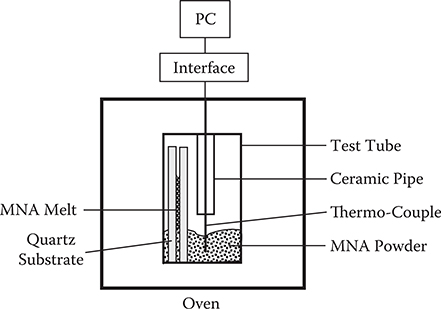
FIGURE 7.9 Crystal growth apparatus with automatic temperature control.
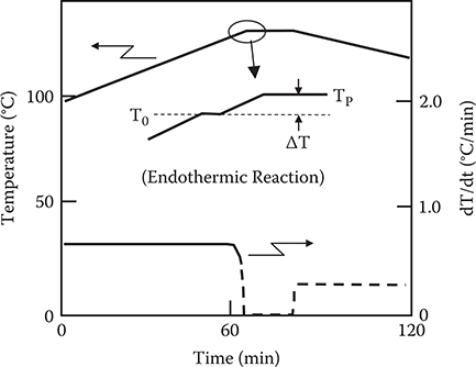
FIGURE 7.10 Temperature-time profile for MNA thin-film crystal growth. From Y. Kubota and T. Yostrimura, “Endothermic reaction aided crystal growth of 2-methyl-4-nitroaniline and their electro-optic properties,” Appl. Phys. Lett. 53, 2579–2580 (1988).
The figure of merit for EO phase retardation (F) of the MNA thin-film crystals was measured by the AC modulation method. In Figure 7.11 the TP dependence of F is shown. As TP decreases toward TM, F increases. When the crystal is prepared so that TM ≈ Tp, the maximum F is twice that of the LiNbO3 crystal. The reproducibility of this value is good as a result of the automatic control of the crystal growth. With annealing (at 118°C for 120 min), F increases from 1.8 × 10⁻¹⁰ to 2.4 × 10⁻¹⁰ m/V. This value is about three times as large as that of the LiNbO3 crystal.
We expect that one of the following reasons is responsible for the variation in F: (1) a change in the molecular structure, (2) a change in the crystal structure, (3) a change in the interaction between neighboring molecules. Differential thermal analysis on MNA revealed no obvious decomposition or degeneration in the molecule. X-ray diffraction analysis showed no Tp dependence of the peak position and the half-width. These results suggest that significant molecular structure degeneration and crystal structure changes did not occur for various values of Tp, and that the variation in F might be caused by reason (3).
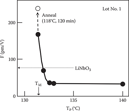
FIGURE 7.11 TP dependence of the figure of merit for electro-optic phase retardation (F). From Y. Kubota and T. Yostrimura, “Endothermic reaction aided crystal growth of 2-methyl-4-nitroaniline and their electro-optic properties,” Appl. Phys. Lett. 53, 2579–2580 (1988).
In Figure 7.12 a relationship between F and a peak position of the photoluminescence spectra (Epeak) is shown. As the peak position shifts to the lower-energy side, F increases. This suggests that changes in F might be attributed to changes in the electronic state of the molecule. The molecular second-order nonlinear susceptibility expressed by Equation (5.23) can be written as follows for the two-level model.
Here, rge is the transition dipole moment from the ground state to the excited state, Δre is the difference in the dipole moment between the excited state and the ground state, and ħωge is the energy gap between the two states. Since the absorption spectra measurements showed little dependence of the energy gap on Tp, the change of dipole moments would cause Tp dependence on F. When crystals are prepared so that some amount of impurity is produced by decomposition, molecular rotations might occur. As a result, the interaction between donors and acceptors of neighboring molecules changes, decreasing the total dipole moment. Consequently, F decreases [10].
Figure 7.13 shows electron distributions in MNA molecules for three arrangements: isolated molecule, three molecules with rotating by θ = 0°, and three molecules with rotating by θ = 35°. The molecular orbitals for each arrangement were calculated by Austin Model 1 (AM1). From Equation (7.9), β of the central molecule was calculated and is shown in Figure 7.14 with bars. When θ increases from 0 to 35°, β decreases. With further increases in θ to 65°, β increases. This result suggests that the interaction between molecules in solids greatly affects the second-order nonlinearity, and confirms the possibility that the TP dependence of F in the MNA crystal is attributed to the change in the interaction between MNA molecules. Also note that, in the configuration of θ = 0°, F is larger than in the isolated molecule. This indicates that enhancement of β occurs by interaction between neighboring molecules depending on the arrangements of those molecules.

FIGURE 7.12 Relationship between F and a peak position of the photoluminescence spectra. From Y. Kubota and T. Yostrimura, “Endothermic reaction aided crystal growth of 2-methyl-4-nitroaniline and their electro-optic properties,” Appl. Phys. Lett. 53, 2579–2580 (1988).
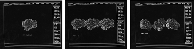
FIGURE 7.13 Influence of arrangement of MNA molecules on electron distributions.
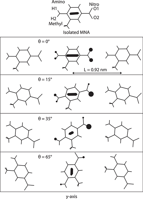
FIGURE 7.14 Influence of arrangement of MNA molecules on β.
Figure 7.15 shows the dependence of F on the purity of the MNA powder used for crystal growth. Here, F is normalized with respect to that of the LiNbO3 crystal. Purity was measured by differential scanning calorimetry (DSC). It is found that F drastically decreases with decreases in the purity of MNA powder to less than 99.9%. The origin of the purity dependence of F might be similar to that of the TP dependence mentioned previously. That is, a small number of impurity molecules will cause the rotation of a large number of molecules.
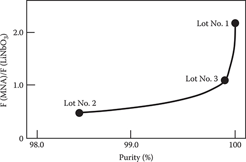
FIGURE 7.15 Dependence of F on the purity of the MNA powder. From Y. Kubota and T. Yostrimura, “Endothermic reaction aided crystal growth of 2-methyl-4-nitroaniline and their electro-optic properties,” Appl. Phys. Lett. 53, 2579–2580 (1988).
7.1.3 POLED POLYMERS AND OPTICAL SWITCHES
7.1.3.1 EO Effects in Poled Polymers
Poled polymers are obtained by applying a poling process to spin-coated polymer films containing nonlinear optical molecules. The typical fabrication process of poled polymers is shown in Figure 7.16. At temperature TP above glass transition temperature Tg,, an electric field is applied to the polymer film. Then, the nonlinear optical molecules in the film rotate to align in the electric field direction. By cooling to room temperature, the aligned orientations of molecules are fixed in the film to generate second-order optical nonlinearity.
EO coefficient r of poled polymers is expressed by the following formula.
Here, β, μ and N are molecular second-order nonlinear susceptibility, electric dipole moment, and concentration of nonlinear optical molecules, respectively. Ep is the poling electric field, Tp is the poling temperature, and kB is the Boltzman constant. f and f0 are given by the following expressions using dielectric constant ε and refractive index n and n∞ .
From Equation (7.10), it is found that r increases by increasing β, μ, N, and Ep, and by decreasing Tp. Figure 7.17 summarizes the influence of β and Tp on r [11]. With decreasing Tp, thermal disturbance during poling is suppressed to improve molecular alignment along the electric fields, resulting in an increase in r. However, low Tp implies low Tg of the polymer, which causes decay of the Pockels effect due to relaxation of aligned orientations of molecules to random orientations (Figure 7.16). This results in a decrease in thermal stability. Thus, in poled polymers, resolving the tradeoff relationship between r and thermal stability is the most important issue.
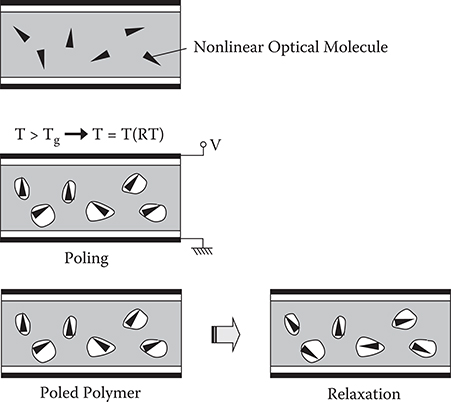
FIGURE 7.16 Fabrication process of poled polymers.
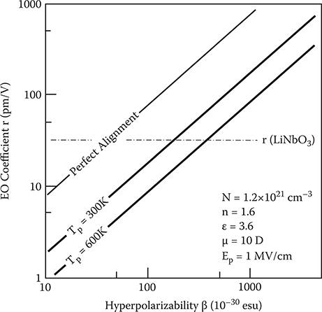
FIGURE 7.17 Influence of β and TP on r in poled polymers.
7.1.3.2 EO Polyimide
Poled polymers with second-order nonlinear optical properties are suitable materials for EO devices because of their low dielectric constants and waveguide processability. In order to improve the thermal stability after poling, polyimide was developed with nonlinear optical molecules of azobenzene dyes attached as side chains [12]. The polymer system with side chains is expected to offer high EO coefficients because of the high-density nonlinear optical molecules and high thermal stability because of the polyimide backbones.
The chemical reaction for side-chain polyimide synthesis is shown in Figure 7.18. As shown in Figure 7.19, obvious thermal decomposition does not occur below 250°C since the absorption peak at 480 nm, which is attributed to the azobenzene dye, is preserved.
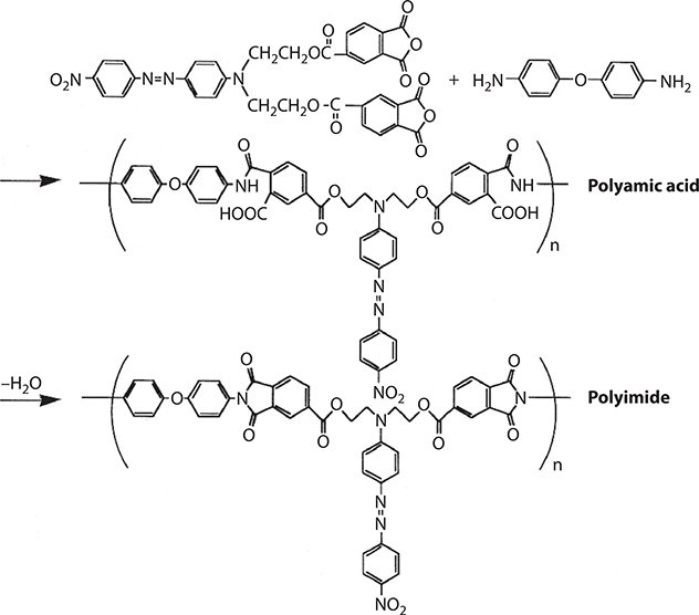
FIGURE 7.18 Chemical reaction for the side-chain polyimide synthesis. From W. Sotoyama, S. Tatsuura, and T. Yoshimura, “Electro-optic side-chain polyimide system with large optical nonlinearity and high thermal stability,” Appl. Phys. Lett. 64, 2197–2199 (1994).
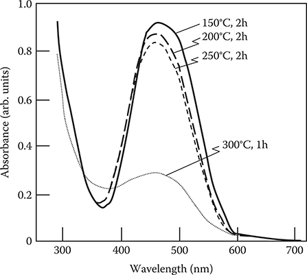
FIGURE 7.19 Absorption spectra of the side-chain polyimide after baking at 150, 200, 250, and 300°C. From W. Sotoyama, S. Tatsuura, and T. Yoshimura, “Electro-optic side-chain polyimide system with large optical nonlinearity and high thermal stability,” Appl. Phys. Lett. 64, 2197–2199 (1994).
The process for EO polyimide fabrication is shown in Figure 7.20. By spin coating, a polyamic acid film was formed on a glass substrate with an indium tin oxide (ITO) electrode. Next, the solvent was removed by baking at 100°C. The polymer film thickness was a few μm. The polyamic acid film was imidized at 250°C for 2h. An Au electrode was deposited on it. Then, the polyimide film was poled by applying electric fields of 170 MV/m between the ITO electrode and the Au electrode at 180°C for 1 h.
The EO coefficient r33, measured by the reflection technique developed by Teng and Man [13], was 10.8 pm/V at 1.3 μm in wavelength. The thermal stability of the EO efficiency of the EO polyimide was tested by keeping the sample at 120°C. As shown in Figure 7.21, after more than 200 h, the EO coefficient of the sample retained nearly 90% of the initial value.
In addition, Figure 7.22 shows the influence of nonlinear optical molecule structures on decay of EO coefficients of poled polymers with epoxy backbones. It is found that the diacetylene structure is preferable to suppress decay than the azobenzene structure.
7.1.3.3 Optical Switches Using EO Polyimide
Figure 7.23 shows a schematic illustration and switching operation of a directional coupler optical switch using the EO polyimide. Figure 7.24 shows a photograph of the optical switch. The devices are fabricated on a conductive Si wafer, which is used as the lower electrode. In this device, the clad part consists of the EO polyimide and the core consists of a passive fluorinated polyimide. When applied voltage V is 0 V, a light beam is guided to one branch of the optical switch. When 500 V is applied, the light beam is picked up to another branch, showing the switching operation. The drive voltage is extremely high. This is attributed to the fact that only a small fraction of the light beam feels the refractive index change that is induced by the EO effect because the EO materials do not exist in the core region, where most of the light beam’s electric fields are confined, but exist in the surrounding clad region.
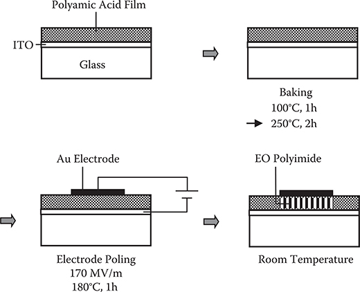
FIGURE 7.20 Process for EO polyimide fabrication.
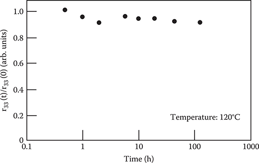
FIGURE 7.21 Relationship between heating time (at 120°C) and EO coefficient of the EO polyimide. From W. Sotoyama, S. Tatsuura, and T. Yoshimura, “Electro-optic side-chain polyimide system with large optical nonlinearity and high thermal stability,” Appl. Phys. Lett. 64, 2197–2199 (1994).
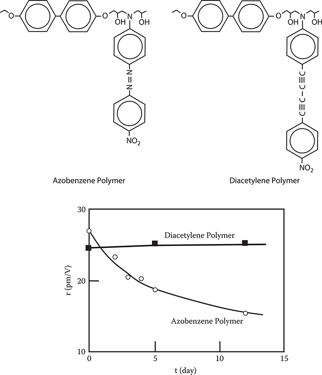
FIGURE 7.22 Influence of nonlinear optical molecule structures on decay of EO coefficients of poled polymers.
7.1.3.4 3-D Optical Switches
To fabricate optical integrated circuits for high-density optical wiring, small light modulators and optical switches in three-dimensional (3-D) optical circuits are required. The vertical directional coupler consisting of two stacked EO polymer waveguides [14] is a candidate for the 3-D optical switch.
The 3-D optical switch with a directional coupler structure is constructed by stacking two polymer waveguides and poling them to create the EO effect in them. The directional coupler has a certain coupling length, which varies according to the electric-field-induced refractive index change of the EO polymer waveguides. Consequently, a laser beam introduced into one of the waveguides is switched between the two waveguides by voltage application.
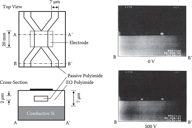
FIGURE 7.23 Schematic illustration and switching operation of an optical switch using the EO polyimide.
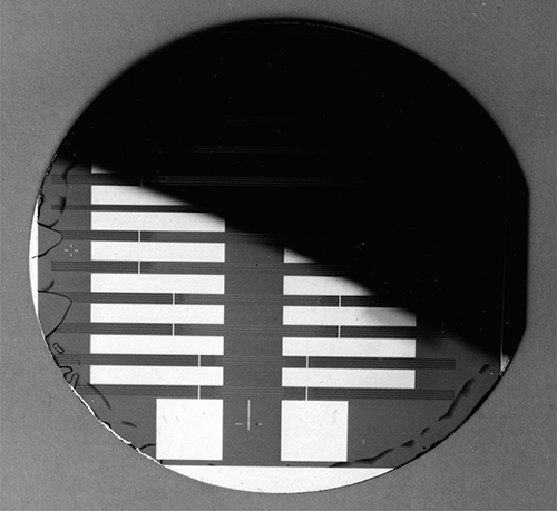
FIGURE 7.24 Photograph of the optical switch using the EO polyimide.
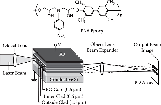
FIGURE 7.25 Structure of the 3-D optical switch, experimental setup, and structure of paranitroaniline-bonded epoxy polymer. From W. Sotoyama, S. Tatsuura, K. Motoyoshi, and T. Yoshimura, “Directional-coupled optical switch between stacked waveguide layers using electro-optic polymer,” Jpn. J. Appl. Phys. 31, L1180–L1181 (1992).
In Figure 7.25, the structure of the 3-D optical switch and experimental setup are shown, as well as the structure of paranitroaniline-bonded epoxy polymer (PNAepoxy) used for the EO core layer. The refractive index of the PNA-epoxy layer is 1.64 before poling. Polyvinylalcohol (PVA) with a refractive index of l.53 is used for the clad layers. These layers are stacked on a conductive silicon wafer by spin coating. Each waveguide layer is considered a single-mode slab waveguide having the same effective index.
A He-Ne laser beam (633 nm) was coupled into the stacked waveguide through the cleaved edge. The scattered light from the top of the waveguide was observed as bright and dark stripes perpendicular to the direction of the propagating light beam, which indicates that the light beam is transfered between the upper and the lower waveguides alternately according to the stripe interval. The stripe interval was about 0.3 mm for the transverse electric (TE)-mode wave, being consistent with the calculated coupling length of 0.34 mm.
A 100-nm-thick planar Au electrode was deposited on top of the stacked layers. The PNA-epoxy core layers were poled by applying 200 V between the substrate and the top Au electrode at 60°C for 5 minutes. After poling, the sample was cleaved for a 5-mm waveguide length, and optical switching measurement was performed in the experimental setup shown in Figure 7.25. A He-Ne laser beam focused by a 100× object lens was coupled to the waveguide in the transverse magnetic (TM)-mode. The exiting beam was collected by a 50× object lens and a 10× beam expander and detected by a photodiode array.
Figure 7.26 shows examples of the output beam line images from the 3-D optical switch detected by the photodiode (PD) array. Two parallel lines spaced about 1 mm apart appear, corresponding to beams from the upper waveguide and the lower waveguide. As Figure 7.27 shows, the intensity pattern of these lines varies when voltage is applied between the substrate and the top electrode, indicating that the light beam switching between layered waveguides is voltage dependent. The switching voltage obtained from the intensity versus voltage characteristics is about 30 V.
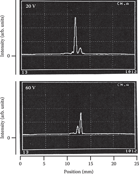
FIGURE 7.26 Output beam line images from the 3-D optical switch detected by the PD array at applied voltage of 20 V and 60 V. Horizontal axis represents position on the PD array. From W. Sotoyama, S. Tatsuura, K. Motoyoshi, and T. Yoshimura, “Directional-coupled optical switch between stacked waveguide layers using electro-optic polymer,” Jpn. J. Appl. Phys. 31, L1180–L1181 (1992).
It should be noted that an optical switch consisting of channel waveguides can be easily constructed in principle using a stripe electrode of a few μm wide. Figure 7.28 shows an example of stacked channel waveguides [15].
For the fabricated device, the switching voltage was 30 V, which is too high for optical interconnect applications, because of the small EO coefficient of the PNAepoxy polymer, r33 = 3 pm/V. The switching voltage can be reduced by improving the polymer, for example, by implementation of the polymer multiple quantum dots (MQDs) fabricated by MLD.

FIGURE 7.27 Output beam line intensity as a function of applied voltage. Solid circle represents intensity of one line and rectangle the other. From W. Sotoyama, S. Tatsuura, K. Motoyoshi, and T. Yoshimura, “Directional-coupled optical switch between stacked waveguide layers using electro-optic polymer,” Jpn. J. Appl. Phys. 31, L1180–L1181 (1992).
7.2 Optical Waveguides Fabricated by Selective Wire Growth
As mentioned in Section 7.1.3, the trade-off relationship between r and thermal stability is the most serious problem in poled polymers. One of the ways to resolve it is to apply selectively aligned polymer wire growth to EO polymer fabrication. This section covers several examples of EO waveguide formation by selectively aligned polymer wire growth utilizing electric fields and anisotropic surface structures.
7.2.1 EO WAVEGUIDES FABRICATED BY ELECTRIC-FIELD-ASSISTED GROWTH
When molecules with sufficiently high reactivities are used in electric-field-assisted growth (described in Section 3.6.3), polymer films could be fabricated at around room temperature. If electric fields are selectively applied to the polymer wire growth regions, nonlinear optical molecules are aligned by the applied electric field and simultaneously polymerized, enabling poled polymer fabrication below the glass transition temperature. In this method, molecules could move rather freely and disordering by thermal disturbance could be reduced to achieve highly oriented poling. This resolves the problem of the trade-off relationship between r and thermal stability.
Electric-field-assisted growth has additional advantages. In conventional poling, during rotation of the molecules, stress and free volume are generated in the surrounding regions. These cause a force to relax the oriented molecules back to the initial random state as shown in Figure 7.16, which decreases the thermal stability of the poled polymers. On the contrary, in the polymer fabricated by electric-field-assisted growth, such stress is not induced because rotation of molecules occurs before polymerization.
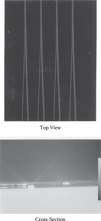
FIGURE 7.28 An example of stacked channel waveguides.
Furthermore, since electric-field-assisted growth is carried out in vacuum, lower impurity concentration is expected. By combining electric-field-assisted growth with MLD, precise molecular rotation controllability as well as thickness controllability and conformability of the film are expected.
7.2.1.1 Epoxy-Amine Polymer
Optical waveguides of EO epoxy-amine polymer [BE/AEANP] were fabricated using a reaction between tetramethyl-biphenylepoxy (BE) and 2(2-aminoethylamino)-5-nitropyridine (AEANP), as shown in Figure 7.29 [16,17]. AEANP, which has a pyridine ring connected to a donor (-NH(CH2)-) and an acceptor (-NO2), is a nonlinear optical molecule. AEANP has a dipole moment and is estimated from the MO calculation to have β about a half of β in p-nitroaniline. Therefore, AEANP could be aligned by electric field application during polymer wire growth in vacuum to produce EO polymer wires.
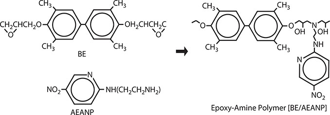
FIGURE 7.29 Reaction for epoxy-amine polymer [BE/AEANP] wire growth.
Epoxy-amine polymer growth was performed with a gas pressure of 5 × 10⁻³ Pa (background pressure of < 10−4 Pa) at a deposition rate of 0.2–0.5 nm/s. The film fabricated at Ts = 30°C was yellow and transparent when the AEANP/BE ratio was 1/1, which is consistent with the polymer structure shown in Figure 7.29.
Figure 7.30 shows infrared spectra of the film and the two molecules. In the film spectrum, the band of the epoxy ring (911 cm−1) becomes very small, that of -NH2 (3367 cm−1) disappears, and that of –OH grows compared to the spectra of AEANP and BE molecules. These changes indicate that polymerization progressed and a polymer film was grown.
To fabricate channel optical waveguides, a thermally oxidized Si wafer with a 1-μm-thick SiO2 clad layer was prepared as the substrate. A1 slit-type electrodes with a 10- and 20-μm gap were formed on the substrate. Epoxy-amine polymer [BE/AEANP], 1.3-μm thick, was grown under electric field applied in the gap region of slit-type electrodes. The applied electric field was 0.2 MV/cm and 0.1 MV/cm for the gap of 20 μm and 10 μm, respectively. Figure 7.31 shows a photograph of the sample for epoxy-amine polymer [BE/AEANP] waveguides.
A He-Ne laser beam (633 nm) was introduced into the epoxy-amine polymer [BE/AEANP] film on the gap region to guide the beam. As shown in Figure 7.32, a streak of the guided beam is observed in the gap region, demonstrating that a low-loss channel waveguide is formed in the gap region. Near-field pattern observation revealed that a guided beam with polarization parallel to the y-axis is bright while a guided beam with polarization parallel to the z-axis is very weak, indicating that the guided beam mainly contains polarization parallel to the y-axis. This result is attributed to AEANP alignment induced by the electric field along the y-axis. The AEANP alignment along the y-axis increases the refractive index for polarization parallel to the y-axis and decreases that for polarization perpendicular to the y-axis (i.e., parallel to the z-axis), resulting in selective confinement of the He-Ne laser beam with y-polarization into the channel optical waveguide. The EO coefficient of the channel waveguide evaluated by a Mach-Zehnder interferometer is approximately 0.1 pm/V at 633 nm.
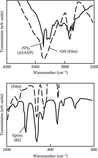
FIGURE 7.30 Infrared spectra of a film and the two molecules. From S. Tatsuura, W. Sotoyama, and T. Yoshimura, “Epoxy-amine polymer waveguide containing nonlinear optical molecules fabricated by chemical vapor deposition,” Appl. Phys. Lett. 60, 1158–1160 (1992).
To confirm the effect of an applied electric field during deposition, channel waveguides were fabricated from the same polymer using electrode poling. After the polymer film deposition, the film was poled with an electric field of 0.2 MV/cm at room temperature and at 66°C. It was found that the EO coefficient of the waveguide formed by electric-field-assisted growth is over 100 times larger than that of the waveguide formed by electrode poling at room temperature and at 66°C.
These results show that molecular alignment and polymerization were accomplished simultaneously during the film deposition and demonstrate the advantage of electric-field-assisted growth.
7.2.1.2 Poly-Azomethine
As mentioned in Section 3.8, conjugated polymers are expected to be high-performance materials for various thin-film photonic/electronic devices. As an example of a functional conjugated polymer device, EO waveguides of poly-AM [o-PA/MPDA] were fabricated by electric-field-assisted growth [18].
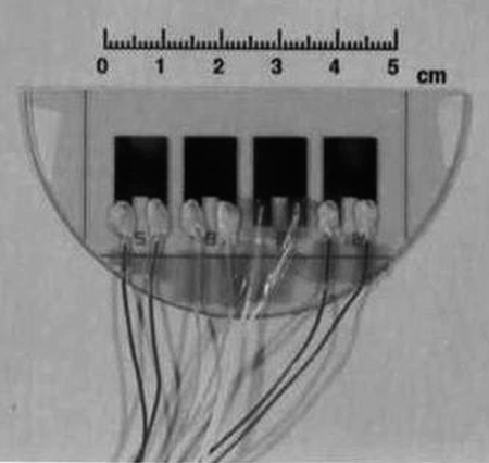
FIGURE 7.31 Photograph of a sample for epoxy-amine polymer [BE/AEANP] waveguides.
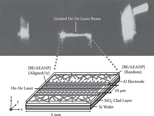
FIGURE 7.32 Guided He-Ne laser beam in a channel waveguide of epoxy-amine polymer [BE/AEANP] grown by electric-field-assisted growth.
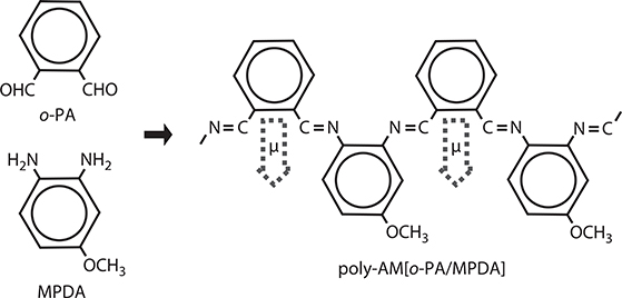
FIGURE 7.33 Reaction for poly-AM [o-PA/MPDA] wire growth. From S. Tatsuura, W. Sotoyama, K. Motoyoshi, A. Matsuura, T. Hayano, and T. Yoshimura, “Polyazomethine conjugated polymer film with second-order nonlinear optical properties fabricated by electric-field-assisted chemical vapor deposition,” Appl. Phys. Lett. 62, 2182–2184 (1993).
Poly-AM [o-PA/MPDA] is formed with the reaction shown in Figure 7.33 using o-phthalaldehyde (o-PA) and 4-methoxy-o-phenylenediamine (MPDA). The methoxy group in MPDA acts as a donor. From the MO calculation it is found that in poly-AM [o-PA/MPDA] wire dipole moments are generated along a direction perpendicular to the wire, and a large β of 3–5 times that of p-nitroaniline is expected.
A thermally oxidized Si wafer with Al slit-type electrodes was prepared as a substrate. The electrodes were about 100-nm thick and the gaps were 5–20 μm wide. Yellow-orange poly-AM [o-PA/MPDA] film with a thickness of 0.8–3.3 μm was grown at a molecular gas pressure of 1−10−1 Pa under an electric field of 0–0.6 MV/ cm in the gap region of the slit-type Al electrodes.
Deposition rate dependence of the peak optical density and the energy gap obtained from the absorption spectra of poly-AM [o-PA/MPDA] is shown in Figure 7.34. As the deposition rate decreases, the peak optical density increases and the energy gap decreases. The results are attributed to an increase in conjugated lengths of poly-AM [o-PA/MPDA] with decreases in the deposition rate. This tendency can be explained because the deposition rate decrease increases the time for o-PA and MPDA to migrate on the substrate surface, meet each other, and then combine with strong bonds.
The polymer film’s refractive index was 1.68 at 633 nm. A He-Ne laser beam was directly coupled to the poly-AM [o-PA/MPDA] film on a thermally oxidized Si wafer with Al slit electrodes. The SiO2 layer was about 1 μm thick. A channel-like beam propagation over 15 mm long was observed in the electrode gap region. The exiting beam’s near-field pattern was bright in TE mode and weak in TM mode. This is attributed to the fact that the benzene ring planes in the polymer wires were aligned parallel to the substrate by the applied electric field.
Figure 7.35 shows EO responses in poly-AM [o-PA/MPDA] obtained with applied electric fields of 0.5 MV/cm and 0 MV/cm during growth. For this experiment, quartz substrates with Ni-Cr slit electrodes were used. The EO effect was measured using a Mach-Zehnder interferometer. The poly-AM [o-PA/MPDA] film was placed in one arm of the Mach-Zehnder interferometer with the film plane perpendicular to a He-Ne laser beam. The polarized direction of the laser beam was in the applied electric field direction in the electrode gap region. For 0.5 MV/cm, clear EO responses are observed in a Mach-Zehnder interferometer while no EO responses were observed for 0 MV/cm. The EO response was observed after heating at 80°C for 5 h; this confirms that the conjugated polymer is thermally stable.
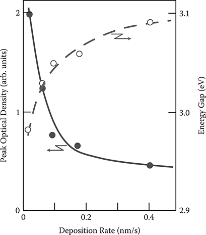
FIGURE 7.34 Deposition rate dependence of the peak optical density and the energy gaps in poly-AM [o-PA/MPDA] grown by electric-field-assisted growth. From S. Tatsuura, W. Sotoyama, K. Motoyoshi, A. Matsuura, T. Hayano, and T. Yoshimura, “Polyazomethine conjugated polymer film with second-order nonlinear optical properties fabricated by electric-field-assisted chemical vapor deposition,” Appl. Phys. Lett. 62, 2182–2184 (1993).
These results demonstrate the possibility that conjugated polymer wires can be used for EO waveguides. By combining the process with MLD, the EO effect of the conjugated polymer wires will be optimized.
7.2.2 CONJUGATED POLYMER WAVEGUIDES FABRICATED ON ANISOTROPIC SURFACE STRUCTURES
EO waveguides of poly-AM [TPA/PPDA] were fabricated by selectively-aligned growth on surfaces with anisotropic structures [19]. A schematic illustration of the waveguide structure is shown in Figure 7.36(a). The SiO underlayer was deposited in waveguide core patterns by vacuum evaporation on a glass substrate that was tilted by 45° along the y-axis as mentioned in Section 3.6.2. The obliquely evaporated SiO film thickness was 200 nm. A poly-AM [TPA/PPDA] film was grown on the substrate by the carrier gas–type organic chemical vapor deposition (CVD) using terephthalaldehyde (TPA) and p-phenylenediamine (PPDA). Growth time was 1 h. The carrier gas flow rate was 4 NL/min. Gas pressure was 100 Pa or more.
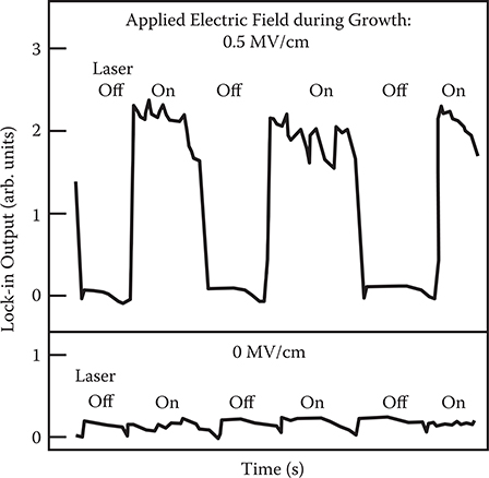
FIGURE 7.35 EO responses in poly-AM [o-PA/MPDA] grown by electric-field-assisted growth. From S. Tatsuura, W. Sotoyama, K. Motoyoshi, A. Matsuura, T. Hayano, and T. Yoshimura, “Polyazomethine conjugated polymer film with second-order nonlinear optical properties fabricated by electric-field-assisted chemical vapor deposition,” Appl. Phys. Lett. 62, 2182–2184 (1993).
Poly-AM deposited all over the substrate surface was selectively aligned along the y-axis on the obliquely evaporated SiO region. In the other region, poly-AM was randomly aligned. Figure 7.36(b) shows a microscope image of the fabricated waveguide. A laser beam of 650 nm in wavelength was introduced into the waveguide of 4-μm core width. It was found that the beam propagates through the waveguide. Thus, waveguide formation using poly-AM [TPA/PPDA] by selectively aligned growth is successfully demonstrated. Again, by combining the process with MLD, the EO effect of the conjugated polymer wires is obtained.
7.2.3 ACCEPTOR SUBSTITUTION INTO CONJUGATED POLYMER WIRES
As shown in Chapter 5, for drastic enhancement of optical nonlinearity of conjugated polymer wires, donor–acceptor substitution into polymer backbones is necessary. We tried a preliminary experiment for the substitution by using TPA for molecule A and 2-nitro-1,4-phenylenediamine (NPDA) for molecule B [5]. As shown in Figure 7.37, NPDA has two –NH2 used for connections with TPA, and –NO2, an acceptor. As Figure 7.38 shows, in the poly-AM [TPA/NPDA] film, the absorption band of NPDA film at 400~600 nm disappears and a new band appears at 400~450 nm, indicating that TPA and NPDA combine to form a polymer. Therefore, in principle, donor–acceptor groups can be introduced into conjugated polymer wires by using molecules that contain groups both for connections and for donor–acceptor.
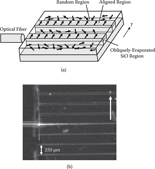
FIGURE 7.36 Poly-AM [TPA/PPDA] waveguide fabricated by selectively-aligned growth on surfaces with anisotropic structures. (a) A schematic illustration of the waveguide structure, and (b) photograph of a guided beam. From K. Matsumoto and T. Yoshimura, “Electro-optic waveguides with conjugated polymer films fabricated by the carrier-gas-type organic CVD for chip-scale optical interconnects,” Proc. SPIE 6899, 98990E-1-9 (2008).
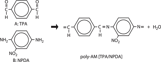
FIGURE 7.37 Molecules and reaction for acceptor-substituted conjugated polymer wire growth.
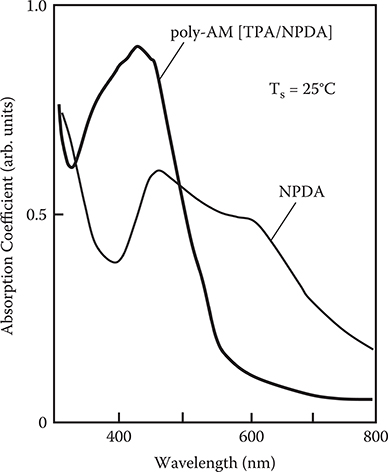
FIGURE 7.38 Absorption spectra of poly-AM [TPA/NPDA] film and NPDA film.
7.3 Nano-Scale Waveguides of Photo-Induced Refractive Index Increase Sol-Gel Materials
One of the important elements for high-speed and small EO devices is the nano-scale optical circuit. It is usually fabricated using Si waveguides [20] with a large refractive index difference between the core and clad. The fabrication process of Si waveguides is well established in the large-scale integrated circuit (LSIs) industry. However, the process is complicated. In order to simplify the process, the silicon nano composite thin film [21] has been developed for etchingless processes. This material is expected to be useful for intrachip optical interconnects because a large refractive index decrease due to UV photo-oxidation of Si atoms is induced by patterned UV light exposure.
The photoinduced refractive index increase (PRI) sol-gel material, which was developed by Nissan Chemical Industries, Ltd., is another promising material for etchingless processes [22]. The distinguished feature of the PRI sol-gel material is the large refractive index increase capability. In spin-coated films of sol-gel materials, the refractive index increases from 1.65 to 1.85 at λ = 633 nm by UV-light exposure and baking, giving rise to a refractive index contrast of ~13%. Although the contrast of 13% is smaller than ~60% in Si waveguides, it is sufficient to provide nano-scale waveguide structures. Thus, the PRI sol-gel material enables us to fabricate high-index contrast (HIC) waveguides without etching/developing processes, simplifying the fabrication processes of the nano-scale waveguides.
In intrachip optical interconnects, 850 nm is the most popular signal light wavelength. With respect to detector sensitivity, blue light is preferable [23]. The short-wavelength light is also preferable to miniaturize optical circuits. For these reasons, we focused our attention on visible wavelength regions, and thus, a He-Ne laser of 633 nm was used for evaluating the optical circuits. The high transmission capability at short wavelengths is a remarkable advantage of the PRI sol-gel material against Si.
Furthermore, by using the PRI sol-gel material, optical circuits consisting of high-index contrast waveguides are available with structures of ultrathin planar films with a thickness of 100 nm order. This is favorable for stacking optical circuits on LSIs and for constructing 3-D optical circuits with stacked films [24,25]. Therefore, the PRI sol-gel material is promising for nano-scale optical circuits, especially for a constituent of small-size optical switches.
In the present section, nano-scale waveguides made of PRI sol-gel material are reviewed [22].
7.3.1 FABRICATION PROCESS
The PRI sol-gel material is a silicon-oxide-based sol-gel material incorporating titanium oxide. The optical waveguide fabrication process is shown in Figure 7.39. On a Si substrate with SiO2 of 2 μm thickness, the sol-gel material was coated and then prebaked for solvent removal.
The layer was selectively exposed to UV light from a high-pressure mercury lamp through a photomask with light intensity of ~5 mW/cm2 and energy of 9000 mJ/cm2. The nominal core pattern width is 1 μm in the photomask. The UV light exposure activates the hydrolytic condensation of the titanium oxide.
Finally, the layer was postbaked at 200°C for 15 min. During postbaking, the hydrolytic condensation proceeds more rapidly in UV light–exposed areas than in unexposed areas, yielding a higher refractive index in the exposed areas than in the unexposed surrounding areas. Thus, the UV light–exposed areas become cores.
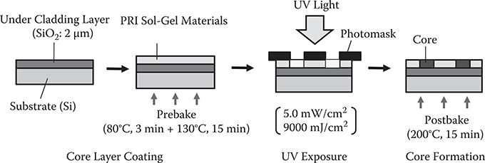
FIGURE 7.39 Fabrication process of optical waveguides using the PRI sol-gel material. From S. Ono, T. Yoshimura, T. Sato, and J. Oshima, “Fabrication and evaluation of nanoscale optical circuits using sol-gel materials with photo-induced refractive index variation characteristics,” J. Lightwave Technol. 27, 1229–1235 (2009).
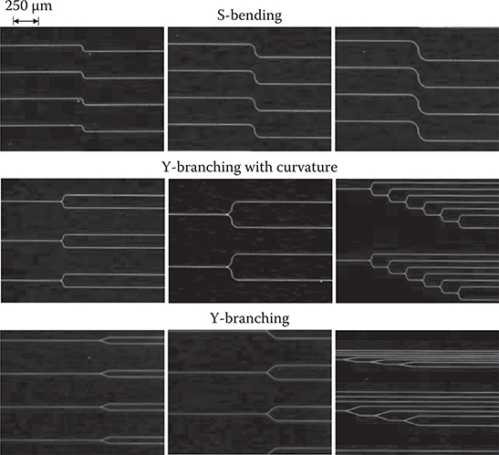
FIGURE 7.40 Photographs of nano-scale optical circuits fabricated using the process shown in Figure 7.39. From S. Ono, T. Yoshimura, T. Sato, and J. Oshima, “Fabrication and evaluation of nano-scale optical circuits using sol-gel materials with photo-induced refractive index variation characteristics,” J. Lightwave Technol. 27, 1229–1235 (2009).
The initial refractive index with no UV light dose, which corresponds to the refractive index of the clad, is 1.65. Refractive index differences between the core and clad (Δn) increases with UV light dose. Δn is saturated to be ~0.2 with a UV light dose of 9000 mJ/cm2. Δn is basically not affected by the prebake and postbake temperature below 200°C. However, high-temperature baking (e.g., over 300°C) induces hydrolytic condensation in unexposed areas, and hence the refractive index contrast between core and clad tends to be reduced with increased baking temperature. Photographs of nano-scale optical circuits fabricated using the process shown in Figure 7.39 are shown in Figure 7.40. The core thickness is ~230 nm and core width is ~1 μm.
7.3.2 LINEAR WAVEGUIDES
Figure 7.41 shows a guided beam and an output beam from a core edge of a linear wave-guide. Propagation loss was 1.86 dB/cm for TE mode (polarization // x-axis) and 1.89 dB/cm for TM mode (polarization // y-axis), indicating small polarization dependence.
Far-field patterns (FFPs) of the output beam from the core edge are shown in Figure 7.42. Spread angles of the output beams, which were determined by the width of the FFPs at a light intensity of 1/e of the maximum height, are 20° and 40° in the core width direction (// x-axis) and in the core thickness direction (// y-axis), respectively, for both TE mode and TM mode. Spot size (spot radius) of the guided beam can be calculated from the spread angle using the following equation.
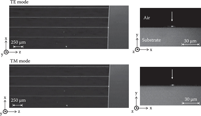
FIGURE 7.41 Photographs of linear waveguides, a guided beam in one of them, and an output beam from the core edge. From S. Ono, T. Yoshimura, T. Sato, and J. Oshima, “Fabrication and evaluation of nano-scale optical circuits using sol-gel materials with photo-induced refractive index variation characteristics,” J. Lightwave Technol. 27, 1229–1235 (2009).
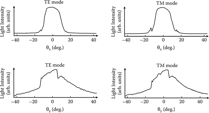
FIGURE 7.42 FFPs of the output beam from the core edge of the linear waveguide. From S. Ono, T. Yoshimura, T. Sato, and J. Oshima, “Fabrication and evaluation of nano-scale optical circuits using sol-gel materials with photo-induced refractive index variation characteristics,” J. Lightwave Technol. 27, 1229–1235 (2009).
Here, w [μm] is the spot size, 2θ (°) is the spread angle of the output beam, and λ [μm] is the guided beam wavelength. The refractive index of the free space (air), where beams emitted from the output propagate, is 1. Spot sizes of guided beams along the x-axis and along the y-axis were calculated to be 0.6 μm and 0.3 μm, respectively, for both TE mode and TM mode. From these results, it is concluded that PRI sol-gel materials can realize guided beam confinement within a cross-sectional area less than 1.0 μm2 with small polarization dependence. Since, roughly speaking, the criterion for core cross-section areas in intrachip optical interconnects is ~1.0 μm2 [26], it is suggested that the PRI sol-gel material can be applied to the internal wiring of chips.
In order to compare the experimental results with theoretical ones, light intensity profiles in the optical waveguides were simulated by the beam propagation method (BPM). The model for the simulation is shown in Figure 7.43. The core thickness is 230 nm, the core width is 1 μm, the refractive index of the core is 1.85, the refractive index of the clad is 1.65, the SiO2 (under clad) thickness is 2 μm, and the refractive index of the under clad is 1.46. The wavelength of the guided beams is 633 nm. The results of the BPM simulation are shown in Figure 7.44. Spot sizes of the guided beams along the x-axis and along the y-axis are, respectively, 0.5 μm and 0.2 μm for both TE mode and TM mode.
The results for spot sizes of the guided beams are summarized in Table 7.1. It is found that the guided beam confinement is slightly stronger in the BPM simulation than in the experiment. The difference might be attributed to Δn. That is, in the fabricated waveguides, Δn is slightly smaller than Δn in the simulation model, that is, less than ~0.2, resulting in an increase in penetration of evanes-cent waves into the clad, which arises from the tunneling effect and an increase in the spot sizes.
It should be noted that Si waveguides enable strong guided beam confinement in cores with a width less than 0.5 μm due to its high core refractive index of ~3.5. However, the high refractive index causes a decrease in the propagation speed of optical signals in Si waveguides. The PRI sol-gel material waveguides, on the other hand, exhibit a faster propagation speed of optical signals by a factor of ~2 compared with Si waveguides because the core refractive index is ~1.85. Considering the trade-off relationship between guided beam confinement and propagation speed, it is expected that the sol-gel material waveguides can preferably be applied to global wiring in chips.
It is expected that further reduction of the core width may be achieved in PRI sol-gel materials by optimization of the fabrication processes for increasing Δn to the theoretical value, which enables nano-scale optical circuits with a core width of less than 1 μm.
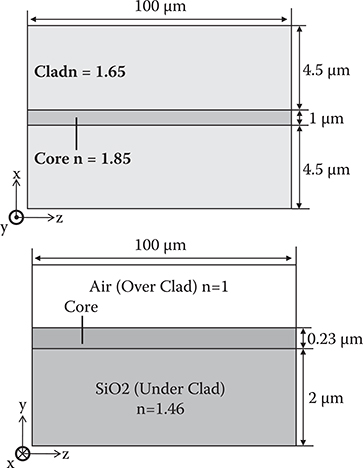
FIGURE 7.43 A model for the BPM simulation. From S. Ono, T. Yoshimura, T. Sato, and J. Oshima, “Fabrication and evaluation of nano-scale optical circuits using sol-gel materials with photo-induced refractive index variation characteristics,” J. Lightwave Technol. 27, 1229–1235 (2009).
7.3.3 s-BENDING AND Y-BRANCHING WAVEGUIDES
S-bending waveguides and guided beams of TE mode in them are shown in Figure 7.45. Output beams from the core edges of the Y-branching waveguides are shown in Figure 7.46 for TE mode. It is found that input beams are divided into two branches with branching angles of 20°, 40°, and 80°. In the photographs in Figure 7.46, there is background in addition to the guided beam spots. Because the 3-μm core radius of the single-mode optical fiber used for introducing light beams into the waveguide cores is much larger than the core sizes of the waveguides and the waveguide length is relatively short, say, less than ~5 mm, considerable beams exist in the clad regions.
The S-bending loss was measured by the following process (Figure 7.47).
The output power P1 at waveguide length L1 is measured.
After cutting the waveguide, output power P2 at waveguide length L2 is measured.
After the waveguide is cut beyond the S-bend, output power P3 at waveguide length L3 is measured.
The output power in units of dBm at each measurement point is plotted against the waveguide length.
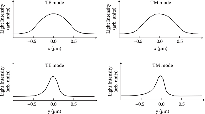
FIGURE 7.44 Light intensity profiles in optical waveguides simulated by BPM. From S. Ono, T. Yoshimura, T. Sato, and J. Oshima, “Fabrication and evaluation of nano-scale optical circuits using sol-gel materials with photo-induced refractive index variation characteristics,” J. Lightwave Technol. 27, 1229–1235 (2009).
TABLE 7.1
Estimated Spot Sizes of Guided BeamsTE Mode
TM Mode
Experiment
0.6 × 0.3
0.6 × 0.3
BPM Simulation
0.5 × 0.2
0.5 × 0.2
Source: S. Ono, T. Yoshimura, T. Sato, and J. Oshima, “Fabrication and evaluation of nano-scale optical circuits using sol-gel materials with photo-induced refractive index variation characteristics,” J. Lightwave Technol. 27, 1229–1235 (2009).
Note: Unit = μm2
(L1, P1) and (L2, P2) are connected with a straight line of y = ax + b. Since slope a gives the propagation loss of the linear waveguide, another straight line of slope a, that is, y = ax + c, is traced on (L3, P3) to represent power vs. waveguide length characteristics before reaching the S-bend part.
Bending loss is obtained from the gap at the S-bend part, c − b, because the gap is caused by guided beam leakage at the S-bend part.
Y-branching loss was also measured by the same method. Bending and Y-branching losses are expressed by the following formula. Bending loss for one bend is one half of the S-bending loss.
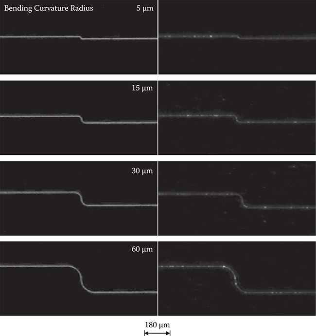
FIGURE 7.45 Photographs of S-bending waveguides and guided beams in them for TE mode. From S. Ono, T. Yoshimura, T. Sato, and J. Oshima, “Fabrication and evaluation of nano-scale optical circuits using sol-gel materials with photo-induced refractive index variation characteristics,” J. Lightwave Technol. 27, 1229–1235 (2009).
The relationship between bending loss and bending curvature radius is shown in Figure 7.48(a). When the radius is increased from 5 μm to 60 μm, the loss is reduced from 0.44 dB to 0.24 dB for TE mode, and from 0.46 dB to 0.26 dB for TM mode. This suggests that the PRI sol-gel materials can provide miniaturized optical circuits with a bending curvature radius of several tens of μm.
The relationship between Y-branching loss and branching angle is shown in Figure 7.48(b). When the angle is decreased from 80° to 20°, the loss is reduced from 1.33 dB to 0.08 dB for TE mode, and from 1.34 dB to 0.12 dB for TM mode. If Y-branching loss of ~ 0.5 dB is permitted, it is expected that PRI sol-gel materials can be used for optical circuits with a branching angle of ~40°.
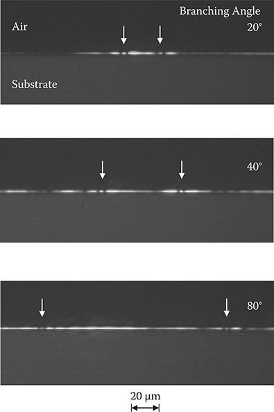
FIGURE 7.46 Photographs of output beams from core edges of Y-branching waveguides for TE mode. From S. Ono, T. Yoshimura, T. Sato, and J. Oshima, “Fabrication and evaluation of nano-scale optical circuits using sol-gel materials with photo-induced refractive index variation characteristics,” J. Lightwave Technol. 27, 1229–1235 (2009).
7.3.4 FINE 3-D STRUCTURES FOR ALL-AIR-CLAD WAVEGUIDES
The PRI sol-gel material becomes insoluble in Al etchant by exposing the material to UV/blue light followed by post-bake. By using this property, fine 3-D structures including all-air-clad waveguides are constructed.
Figure 7.49(a) shows an example of the process for fabricating 3-D waveguide structures. After patterned Al films are deposited on a substrate, a PRI sol-gel film is spin-coated on it. Through a photomask, the sol-gel film is exposed to UV light with a pattern of waveguide cores and is postbaked. By putting the sample in an Al etchant, the unexposed regions of the sol-gel film and the Al film are solved. Thus fine 3-D patterns for 3-D waveguide structures are completed. Figure 7.49(b) shows a scanning electron microscope (SEM) image of an all-air-clad waveguide with a spacer fabricated by the process shown in Figure 7.49(a).
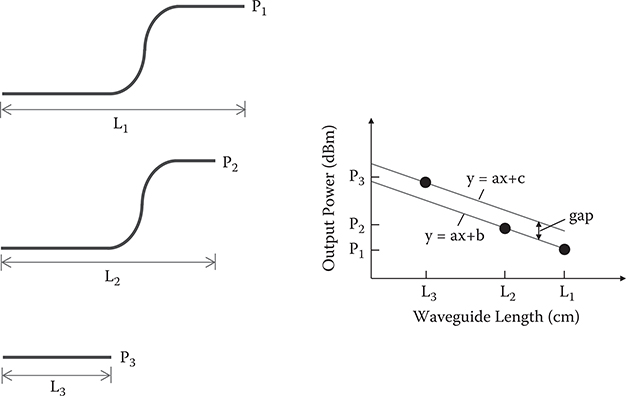
FIGURE 7.47 Evaluation procedure for bending loss. From S. Ono, T. Yoshimura, T. Sato, and J. Oshima, “Fabrication and evaluation of nano-scale optical circuits using sol-gel materials with photo-induced refractive index variation characteristics,” J. Lightwave Technol. 27, 1229–1235 (2009).
7.4 Self-Organized Lightwave Network (Solnet) for Self-Aligned Optical Couplings and Vertical Waveguides
When many thin-film photonic devices are integrated in OE systems such as optical interconnect, optical switching, and solar energy conversion systems, there will be an ever-increasing number and density of optical couplings between the photonic devices, requiring enormous effort for assembly with micron or submicron accuracy. To resolve the problem, the self-organized lightwave network (SOLNET) was proposed [24,27, 28, 29 and 30]. SOLNET enables us to construct self-aligned coupling optical waveguides between misaligned devices.
7.4.1 THE SOLNET CONCEPT
Figure 7.50 shows the SOLNET concept [24,27–30]. Optical devices such as optical waveguides, optical switches, reflectors, vertical cavity surface emitting lasers (VCSELs), photodiodes (PDs), and so on are placed in a photo-induced refractive index increase (PRI) material such as photo-polymers for holography, PRI sol-gel materials, photo-definable materials, or photo-refractive crystals, whose refractive index increases with write-beam exposure. By introducing write beams into the PRI material from optical devices, the refractive index distribution of the material continuously changes time by time. The write beam propagation is affected by the varying refractive index distribution, which is generated by the write beams themselves.
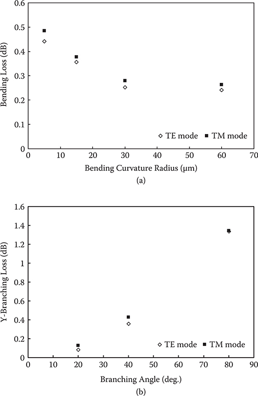
FIGURE 7.48 (a) Relationship between bending loss and bending curvature radius. (b) Relationship between Y-branching loss and branching angle. From S. Ono, T. Yoshimura, T. Sato, and J. Oshima, “Fabrication and evaluation of nano-scale optical circuits using solgel materials with photo-induced refractive index variation characteristics,” J. Lightwave Technol. 27, 1229–1235 (2009).
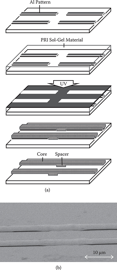
FIGURE 7.49 (a) Process for fabricating 3-D waveguide structures with the PRI sol-gel material. (b) A SEM image of a 3-D waveguide structure for fabricating all-air-clad waveguide with spacers. (This SEM image was provided by T. Sato and J. Oshima.)
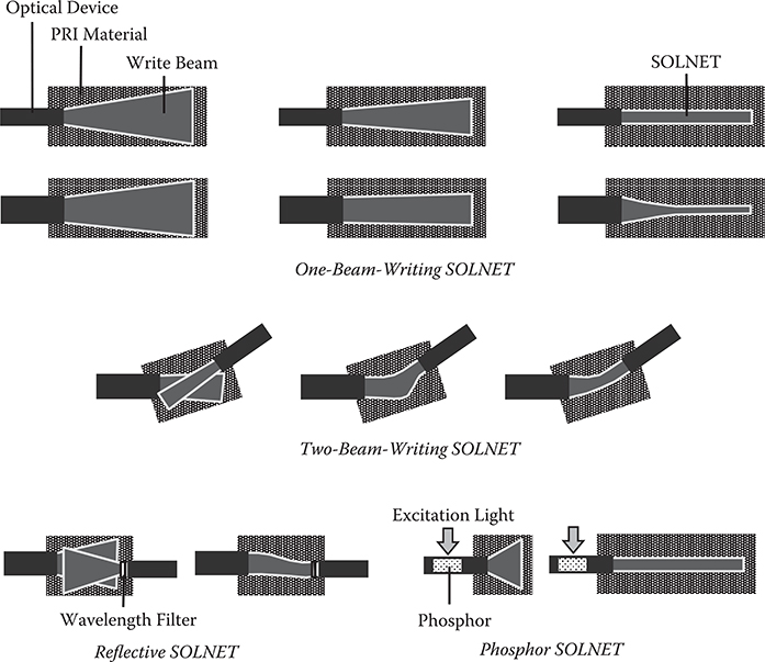
FIGURE 7.50 The SOLNET concept.
In one-beam-writing SOLNET, a write beam is introduced into PRI material from an optical device edge. By the self-focusing effect in the PRI material, the write beam is concentrated along the propagation axis to construct a straight path, forming an optical waveguide with a mode size close to that of the optical device. When a large-mode-size write beam is introduced, the write beam is focused along the propagation axis with a reduced diameter, resulting in a downtaper waveguide that has a smaller mode size at the end than the optical device.
In two-beam-writing SOLNET, two write beams are introduced from two different optical devices. The two beams are attracted each other in PRI material, and merge into one optical waveguide by self-focusing, constructing a coupling optical waveguide between the two optical devices automatically. Even when there is offset in position, offset in angle, and mode size mismatching between the devices, the write beams gradually merge into one, achieving self-aligned coupling between the misaligned devices.
The two-beam-writing SOLNET can be extended to multi-beam-writing SOLNET, in which write beams from two, three, or more optical devices are introduced into the PRI material to achieve self-aligned optical couplings between two, three, or more devices.
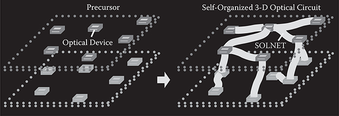
FIGURE 7.51 Concept of the self-organized 3-D optical circuit based on SOLNET.
Reflective SOLNET (R-SOLNET) simplifies the two-beam-writing SOLNET fabrication process. One of the two write beams from optical devices is replaced with a reflected write beam from a reflective element such as a wavelength filter and a mirror on the core facet of the optical device.
In phosphor SOLNET, write beams are generated from phosphor doped in optical waveguides in the devices by exposing the phosphor to excitation light. Phosphor SOLNET and R-SOLNET enable SOLNET construction even when the write beams cannot transmit in the devices, such as photodetectors, laser diodes, and optical switches made of narrow-band-gap materials.
Figure 7.51 shows a concept of the self-organized 3-D optical circuit based on SOLNET. After a precursor is built with optical devices distributed three-dimensionally, optical waveguides are formed between the devices automatically by write beams emitted from some of the optical devices or write beams from outside to construct self-aligned optical waveguides three-dimensionally.
7.4.2 PROOF OF CONCEPT OF SOLNET
7.4.2.1 One-Beam-Writing SOLNET
For an observation of waveguide construction in a free space filled with PRI materials [27,28], the following setup was made. A single-mode optical fiber for 1.3-μm wavelength with a core diameter of 9.5 μm was put in a photo-polymer with PRI effect. A white light beam (HOYA ML-150) of 80 nW was introduced from the fiber to the photo-polymer. A waveguide core was grown from the optical fiber edge along the light propagation axis, to form a straight waveguide. An interference microscopic photograph of SOLNET constructed by 2-minute exposure is shown in Figure 7.52. The line stretched from the edge of the optical fiber is the waveguide core of SOLNET where the refractive index is higher than the surrounding area. The stretched waveguide has a width that is almost the same as the fiber core diameter, indicating the proof-of-concept for one-beam-writing SOLNET.

FIGURE 7.52 Experimental demonstration of one-beam-writing SOLNET. From T. Yoshimura, J. Roman, Y. Takahashi, W. V. Wang, M. Inao, T. Ishituka, K. Tsukamoto, K. Motoyoshi, and W. Sotoyama, “Self-organizing lightwave network (SOLNET) and its application to film optical circuit substrates,” IEEE Trans. Comp., Packag. Technol. 24, 500–509 (2001).
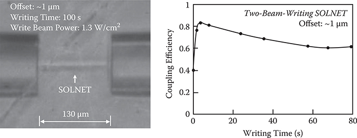
FIGURE 7.53 Experimental demonstration of two-beam-writing SOLNET. From T. Yoshimura, A. Hori, Y. Yoshida, Y. Arai, H. Kurokawa, T. Namiki, and K. Asama, “Coupling efficiencies in reflective self-organized lightwave network (R-SOLNET) simulated by the beam propagation method,” IEEE Photon. Technol. Lett. 17, 1653–1655 (2005).
7.4.2.2 Two-Beam-Writing SOLNET
Two-beam-writing SOLNET was constructed between two optical fibers with a 9.5-μm core diameter placed on a glass substrate with a lateral misalignment of ~1 μm [31]. The gap of 130 μm between them was filled with a photo-polymer made of acrylic/epoxy components developed by JSR Corporation [32]. The acrylic component contains an aromatic diacrylate with a high refractive index and a radical photo-initiator. The epoxy component contains an aliphatic diep-oxide and a photoacid generator. The refractive index is 1.53 and 1.51 for the acrylic and epoxy components, respectively. The mixing ratio of the two components is 50:50 in wt%. The acrylic component exhibits larger reactivity than the epoxy component upon irradiation of light in the range of wavelength below 400 nm, inducing the PRI phenomena. The photo-polymer gives rise to a maximum refractive index change of around 0.02. The energy density required for saturation is ~6 J/cm2 [32].
A self-organized optical waveguide formed by 100-s exposure is shown in Figure 7.53. Write beams of 1.3 W/cm2 from a high-pressure mercury lamp were introduced from the two optical fibers into the photo-polymer. The coupling efficiency measured using 1.3-μm signal beams increases with write beam exposure to reach a maximum over 80%.
7.4.2.3 R-SOLNET
Figure 7.54 shows a schematic illustration of Y-branching R-SOLNET [33]. A write beam from an input optical waveguide and reflected write beams from two wavelength filters on the core facets of two output optical waveguides overlap near the wavelength filters. In the overlap regions, the refractive index of the PRI material increases, pulling the write beams to the wavelength filter locations more and more. We call this effect the pulling water effect. Finally, by self-focusing, self-aligned coupling optical waveguides are formed between the input optical waveguide and the two output optical waveguides.
In order to demonstrate the proof of concept of R-SOLNET experimentally, we carried out R-SOLNET formation between a multimode (MM) optical fiber with a core diameter of 50 μm and a mirror deposited on a facet of an optical fiber [33]. Figure 7.55(a) shows the experimental setup. The MM optical fiber and the mirror are placed in a photo-polymer with a gap of ~800 μm and an angular misalignment of 3° between the MM optical fiber direction and the surface-normal direction of the mirror. The photo-polymer of acrylic/epoxy components was the same as that used for the two-beam-writing SOLNET construction.
Figure 7.55(b) shows a photograph of the MM optical fiber and the optical fiber with the Al mirror on the facet in the photo-polymer. When a write beam from a high-pressure mercury lamp was introduced from the MM optical fiber into the photo-polymer, an R-SOLNET was formed. It is found from Figure 7.55(c) that a probe beam of 650 nm in wavelength, which is introduced from the MM optical fiber, propagates in the optical waveguide of the R-SOLNET. The core width of the R-SOLNET is found to be about 50 μm, which is close to that of the MM optical fiber.
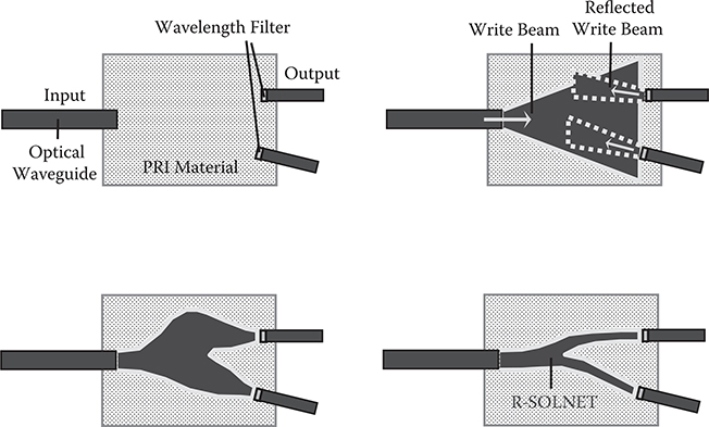
FIGURE 7.54 Schematic illustration of Y-branching R-SOLNET. From T. Yoshimura and H. Kaburagi, “Self-organization of optical waveguides between misaligned devices induced by write-beam reflection,” Appl. Phys. Express 1, 062007-1-3 (2008).
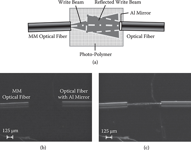
FIGURE 7.55 An experiment of R-SOLNET formation with angular misalignment of 3°. (a) Experimental setup, (b) a photograph before SOLNET formation, and (c) a photograph after SOLNET formation. From T. Yoshimura and H. Kaburagi, “Self-organization of optical waveguides between misaligned devices induced by write-beam reflection,” Appl. Phys. Express 1, 062007-1-3 (2008).
If the pulling water effect does not exist, two optical waveguides of SOLNET with a directional difference of 6° should be formed from the mirror by the incident write beam and the reflected write beam. However, in the photograph shown in Figure 7.55(c), only one bow-shaped optical waveguide of the SOLNET is observed. This indicates that a self-aligned optical waveguide of the R-SOLNET is formed due to the pulling water effect induced by the reflected write beam from the mirror.
Figures 7.56(a) shows the experimental setup for the R-SOLNET with a lateral offset [33]. An MM optical fiber and an optical fiber with an Al mirror are placed with an offset of 30 μm in the photo-polymer (Figure 7.56(b)). When a write beam was introduced from the MM optical fiber into the photo-polymer, the R-SOLNET was formed, connecting the MM optical fiber to the misaligned mirror. It is found from Figure 7.56(c) that a probe beam of 650 nm in wavelength propagates in the S-shaped self-aligned optical waveguide of the R-SOLNET with a core width of about 50 μm.
It is noticed that the R-SOLNET is connected to the upper part of the fiber facet. As can be seen from Figure 7.56(d), the mirror is not deposited uniformly on the fiber facet, but is deposited partially. This is the reason why the R-SOLNET is pulled to the upper part. Actually, trace of the SOLNET is found on the upper part of the fiber facet, where the mirror exists.
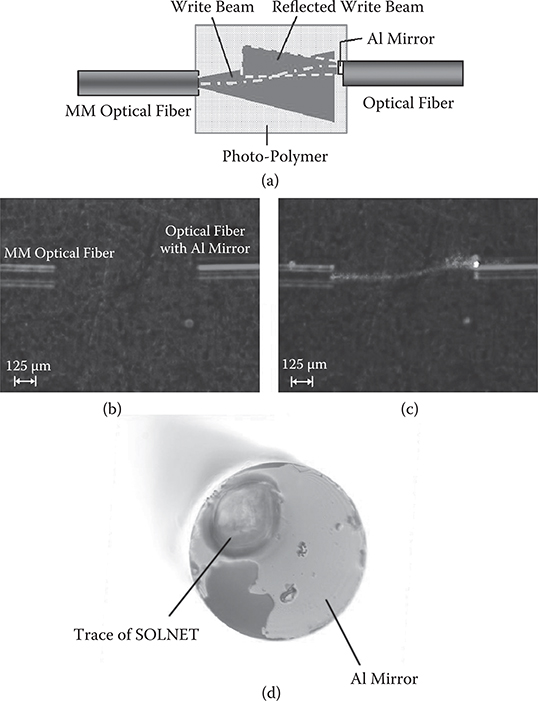
FIGURE 7.56 An experiment of R-SOLNET formation with lateral offset of 30 μm. (a) Experimental setup, (b) a photograph before SOLNET formation, (c) a photograph after SOLNET formation, and (d) a photograph of the Al mirror on the fiber facet. From T. Yoshimura and H. Kaburagi, “Self-organization of optical waveguides between misaligned devices induced by write-beam reflection,” Appl. Phys. Express 1, 062007-1-3 (2008).
In addition, we simulated R-SOLNET formation by the finite difference time domain (FDTD) method for a model with two wavelength filters [33,34]. The model and results are shown in Figure 7.57. An input optical waveguide with a core width of 2 μm and two output optical waveguides with a core width of 0.5 μm are placed in a PRI material with a gap of 10 μm. The output optical waveguides are misaligned by 0.5 μm from the input optical waveguide. The refractive index of the core and clad regions are 1.5 and 1, respectively. The refractive index of the PRI material changes from 1.5 to 1.8 with write beam exposure. Dielectric multilayer wavelength filters on the core facets of the output optical waveguides reflect write beams of 650 nm in wavelength. The filters consist of an 80-nm-thick layer with a refractive index of 1.5 and an 80-nm-thick layer with a refractive index of 2.5. The total layer count is four.
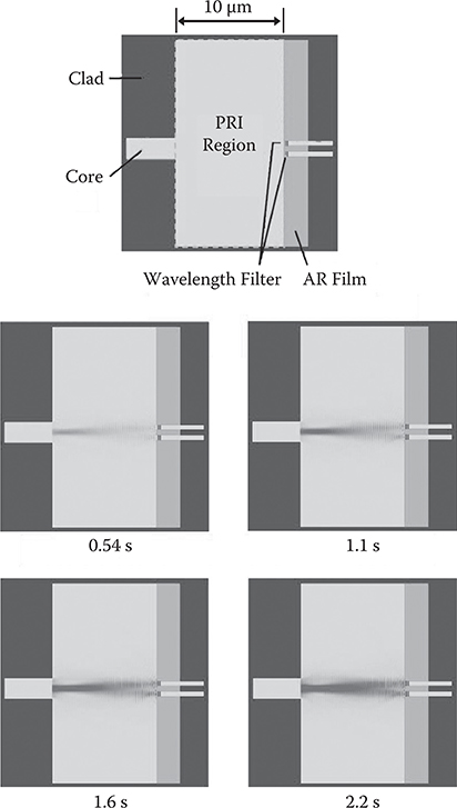
FIGURE 7.57 R-SOLNET formation simulated by the FDTD method for a model with two wavelength filters. From T. Yoshimura and H. Kaburagi, “Self-organization of optical waveguides between misaligned devices induced by write-beam reflection,” Appl. Phys. Express 1, 062007-1-3 (2008).
The simulation procedure is as follows. First, the initial refractive index distribution for the calculated region is input into a data file. Since the refractive index of the PRI material changes with time, the refractive index distribution is rewritten at each time step with a duration of Δt. Energy density of the write beam introduced into the PRI material over Δt [s] is (1/2) εE2vΔt, where, E [V/m] is the electric field of the write beam, ε [J/(mV2)] is the dielectric constant, and v [m/s] is the light velocity. Then, Δn is expressed as
Here, γ [m2/J] is related to the sensitivity of the PRI material. For simplicity, it is assumed that the refractive index changes in proportion to the write beam exposure until it reaches the saturation limit.
In real systems, the typical response time of PRI materials ranges from around a few seconds to a few minutes. In the FDTD method, however, it is difficult to carry out calculations with such long time durations because Δt should be sub-ps. So, in the simulations we rescaled the time parameter to Δt’ as follows.
where, Δt’ = Δt × 1012 and γ’ = γ × 10−12.
The electric field of light sources is expressed as follows.
Here, ω0 is the angular frequency of the light wave and ω0Tω = 4π.
The parameters used in the calculation are as follows. Mesh sizes are Δx = Δy = 20 nm and Δt = 0.0134 ps. Amplitude of the electric field E0 is 10 V/m, which corresponds to a power density of 13 nW/cm2 for ε and v in vacuum. γ’ is 1 m2/J with a saturation limit of 0.3.
It can be seen from Figure 7.57 that Y-branching self-aligned coupling optical waveguides are formed by the pulling water effect. This suggests that a plurality of optical devices can be connected automatically in PRI materials by putting reflective materials such as wavelength filters on the core facets. Coupling optical waveguides of R-SOLNET are led to the reflective materials locations. These results lead us to believe that R-SOLNET is effective in forming self-aligned optical couplings in micro/nano-scale optical circuits.
7.5 Resource-Saving Heterogeneous Integration
7.5.1 CONCEPT OF PL-PACK WITH SORT
In order to integrate various types of thin-film photonic/electronic devices, a low-cost heterogeneous integration process is required. The photolithographic packaging with SORT (PL-Pack with SORT) shown in Figure 7.58 is a promising candidate [35,36]. The total process flow of PL-Pack with SORT is as follows:
Prepare a substrate (LSI, MCM, removable substrate, etc.).
Place thin-film devices on the substrate by SORT.
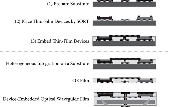
FIGURE 7.58 Total process flow of PL-Pack with SORT. From T. Yoshimura, K. Kumai, T. Mikawa, O. Ibaragi, and M. Bonkohara, “Photolithographic packaging with selectively occupied repeated transfer (PL-Pack with SORT) for scalable optical link multi-chip-module (S-FOLM),” IEEE Trans. Electron. Packag. Manufact. 25, 19–25 (2002).
Embed the thin-film devices in an insulator layer followed by pads/electrodes/vias formation.
Thus, heterogeneous integration is completed on a substrate to provide an OE-LSI, OE-MCM, and so on. When the device-embedded film is removed from the substrate, an OE film is obtained. When combining the process (steps 1–3) with optical waveguide formation, a device-embedded optical waveguide film is obtained.
The most critical part is SORT in step (2). Figure 7.59 shows an outline of SORT. For simplicity, two kinds of devices are considered, although in general many kinds of different thin-film devices are integrated. The process flow is as follows. The Device I array and Device II array are respectively grown with a pitch of d on growth wafer I and growth wafer II. The devices are separated by boundary grooves. All the Devices I are picked up on a pick-up substrate at one time by, for example, epitaxial lift-off (ELO) [37,38], followed by pretransfer to a supporting substrate, Sub I. Similarly, Devices II are pretransferred to Sub II. The distribution patterns of the devices on Sub I and Sub II are respectively designed to match the pad distribution patterns for Devices I and Devices II on the final substrate. The devices left on the pick-up substrates are provided to another Sub I and Sub II.
For final transfer, Sub I is attached on a final substrate, where catch-up pads with a pitch of pP are formed, to selectively place Devices I at sites for Device I on the final substrate. Then, Sub II is attached on the final substrate, to place Devices II at sites for Device II. Sub I and Sub II are further attached to other final substrates, or other places of the final substrate, to provide Devices I and Devices II. By repeating the procedure, all the devices on Sub I and Sub II are transferred to final substrates.
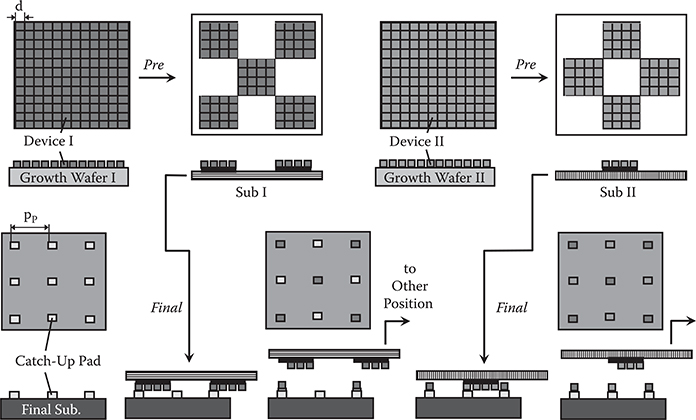
FIGURE 7.59 SORT for integration of two kinds of devices. From T. Yoshimura, M. Ojima, Y. Arai, and K. Asama, “Three-dimensional self-organized micro optoelectronic systems for board-level reconfigurable optical interconnects: performance modeling and simulation,” IEEE J. Select. Topics in Quantum Electron. 9, 492–511 (2003).
For the case shown in Figure 7.59, there are 4 × 4 = 16 devices corresponding to one catch-up pad. This implies that one supporting substrate can provide devices to 16 final substrates. Two supporting substrates are available for Device I and II, respectively, indicating that 32 final substrates, on which Devices I and II are distributed with a desired configuration, can be obtained from a growth wafer I and a growth wafer II.
A marker alignment procedure can be applied to the device transfer process by using an aligner. SORT can stably be performed by using an adhesive whose adhesion strength is controlled with an adhesion strength hierarchy or dynamic adhesion strength control. In the former, the adhesion strength is increased in steps. In the latter, adhesion strength is controlled during the process by, for example, using UV light exposure. For fabrication of OE LSIs, OE boards, or 3-D OE LSIs, Devices I and II could be light modulators, VCSELs, and PDs. For fabrication of three- dimensional micro-optical switching system (3D-MOSS), Devices I and II could be optical switches of polymer MQD, lead lanthanum zirconate titanate (PLZT), or III-V epitaxial films, wavelength filters, photonic crystals, waveguide lenses of TixSiyO thin films, and so on, for example.
7.5.2 ADVANTAGES OF PL-PACK WITH SORT
A schematic illustration for structural comparison between PL-Pack with SORT and conventional flip-chip (FC) bonding is shown in Figure 7.60 for the case of devices made of III-V materials, typically, VCSELs and PDs. In FC bonding, a bulk chip of III-V material is put on a substrate. In PL-Pack with SORT, an OE film in which III-V epitaxial material thin-film flakes with length and width of d are embedded with a pitch of pP, is put on a substrate. The difference brings remarkable advantages to the structure built by PL-Pack with SORT over FC bonding [35,36].
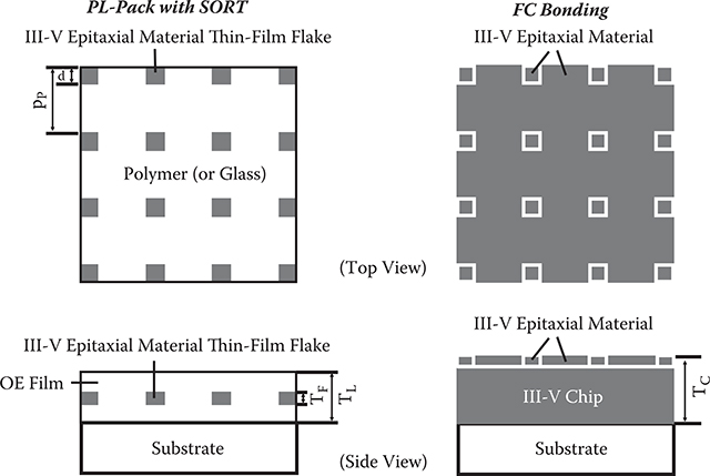
FIGURE 7.60 Schematic illustration of structural comparison between PL-Pack with SORT and conventional FC bonding. From T. Yoshimura, M. Ojima, Y. Arai, and K. Asama, “Three-dimensional self-organized micro optoelectronic systems for board-level reconfigurable optical interconnects: performance modeling and simulation,” IEEE J. Select. Topics in Quantum Electron. 9, 492–511 (2003).
7.5.2.1 Resource Saving
The first advantage of PL-Pack with SORT is its resource-saving characteristics. In FC bonding, the whole area is occupied by expensive III-V epitaxial materials. In PL-Pack with SORT, on the other hand, the epitaxial materials exist only at necessary sites. The III-V epitaxial material saving effect can be measured by the material saving factor (MSF) of PL-Pack with SORT defined by
Here, RSORT and RFC Bonding represent III-V epitaxial material consumption in PL-Pack with SORT and in FC bonding, respectively. Device length and width d and pitch pP in the III-V chips/OE films shown in Figure 7.60, respectively, correspond to the device pitch on a growth wafer and the catch-up pad pitch shown in Figure 7.59. Figure 7.61(a) shows MSF as a function of d for various pP. When pP is 100 μm, MSF equals 1 for d of 100 μm. This implies that whole area of the OE film prepared by PL-Pack with SORT is occupied by III-V epitaxial materials since pP is equal to d. MSF increases with an increase in pP and with a decrease in d, reaching more than 100~1000.
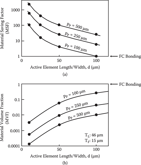
FIGURE 7.61 (a) MSF and (b) MVF as a function of d for various pP. From T. Yoshimura, M. Ojima, Y. Arai, and K. Asama, “Three-dimensional self-organized micro optoelectronic systems for board-level reconfigurable optical interconnects: performance modeling and simulation,” IEEE J. Select. Topics in Quantum Electron. 9, 492–511 (2003).
The resource-saving characteristics of PL-Pack with SORT results in cost reduction of OE systems such as the scalable film optical link module (S-FOLM) described in Section 8.1. Based on the cost versus active element pitch characteristics presented by Stirk et al. for an OE module with a VCSEL array [39], the impact of PL-Pack with SORT on cost can be estimated. As the 0th approximation, costs are assumed to be the same for PL-Pack with SORT and FC bonding, except for III-V epitaxial material cost. Due to the epitaxial-material saving effect in PL-Pack with SORT, module cost is reduced with a decrease in d. For example, in the case that pP and d are, respectively, 200 μm and 50 μm, a cost reduction of ~1/6 is expected. By further decreasing d, a cost reduction of <1/10 might be expected.
7.5.2.2 Process Simplicity
The second advantage of PL-Pack with SORT is process simplicity in heterogeneous integration of thin-film devices, which results in a cost reduction. In FC-bonding-based packaging, generally, different kinds of OE devices should be fabricated on the same chip, which requires a sophisticated film growth method, which raises fabrication cost. In PL-Pack with SORT, as shown in Figure 7.59, heterogeneous integration can be performed by delivering OE devices from a set of wafers. On individual wafers, arrays containing same kind of devices are grown by simple growth method, contributing to cost reduction.
Furthermore, SORT can remove the conventional FC bonding–based packaging to achieve heterogeneous device integration only by semiconductor device fabrication processes, that is, all-photolithographic processes. These features are effective on cost reduction of OE systems.
7.5.2.3 Thermal Stress Reduction
The third advantage of PL-Pack with SORT is the potential to reduce thermal stress. As an example, consider a case where a 2-D VCSEL array of L2 μm2, in which VCSELs are located with a pitch of pP μm, is put on a plastic substrate. For FC bonding, an L2-μm2 bulk III-V chip of TC-μm thick is mounted on the substrate. For PL-Pack with SORT, an L2-μm2 OE film of TL-μm thick, where TF-μm-thick III-V epitaxial material thin-film flakes with d2 μm2 area are embedded with a pitch of pP μm, is mounted on a plastic substrate.
In FC bonding, due to the large difference in the coefficient of thermal expansion (CTE) between III-V material and plastics, as well as due to the large thickness of a III-V chip with a large Young’s modulus, a large thermally induced stress between the chip and the substrate is induced as is well known. In PL-Pack with SORT, compared with FC bonding, the thickness of the III-V material block is reduced by a factor of TF/TC and the area by a factor of d2/L2, indicating that the individual III-V material block volume is reduced by a factor of (TF/TC)(d2/L2). For a case that TF = 15 μm, TC = 500 μm, d = 20 μm, and L = 10,000 μm, roughly speaking, the power inducing the stress at the boundary is reduced by seven orders of magnitude in PL-Pack with SORT.
Figure 7.61(b) shows a material volume fraction (MVF) of III-V material in an OE film, which is defined by
For a case where d = 20 μm, TF = 15 μm, pP = 200 μm, and TL = 46 μm, MVF is calculated to be 0.003, suggesting that the CTE of the OE films is close to that of the host matrix polymer with small Young’s modulus. Thus, the stress between the OE film and the plastic substrate is drastically reduced compared with that between the III-V chip and the plastic substrates. Furthermore, basically, no large thermal expansion difference arises between OE films because the CTE of the film is almost defined by the host matrix polymer. Therefore, it is expected that thermally induced displacement may be neglected in S-FOLM where films are pinned by electrical pad connections.
7.5.3 EXPERIMENTAL DEMONSTRATIONS OF SORT
7.5.3.1 SORT of Polymer Waveguide Lenses
The SORT process for polymer waveguide lenses is shown in Figure 7.62 [40]. On a glass substrate, Al patterns of 50 nm thickness with apertures of waveguide lens shapes were formed to make a “built-in mask,” followed by spin-coating of a polyvinylalcohol (PVA) film 10 μm thick. After drying the PVA in ambient atmosphere at room temperature for 1 h, an acrylic photo-definable material film was spin-coated on it with a thickness of 40 μm. The film was exposed to UV light from a high-pressure mercury lump of 400 mJ/cm2 through the built-in mask to form a polymer waveguide lens array by developing. The waveguide lens diameter is 300 μm, and the pitch in the array is 450 μm. For picking up, a supporting substrate, which is a glass substrate covered with an adhesive film (GelPak film-×8 provided by GelPak), was attached on the top of the polymer waveguide lens array. By solving the PVA film in water, the polymer waveguide lens array was picked up to the supporting substrate.
The photograph on the top in Figure 7.63 represents the polymer waveguide lens array on the adhesive film of the supporting substrate. A final substrate was prepared by exposing a glass substrate covered with a UV-curable-material-coated film (UV tape UE-111AJ provided by Nitto Denko) to UV light from a high-pressure mercury lamp of 180 mJ/cm2 through a photo-mask. The adhesion strength of the exposed region decreased by more than one order of magnitude compared with the unex-posed region, providing a final substrate with catch-up sites having stronger adhesion strength than the surrounding area. For transfer, using the SORT equipment shown in Figure 7.64, the polymer waveguide lens array on the supporting substrate was attached to the final substrate, and then the two substrates were detached to each other. As shown in the photograph on the bottom in Figure 7.63, the polymer waveguide lens was transferred selectively onto the catch-up site of the final substrate. This demonstrates the feasibility of the SORT process.
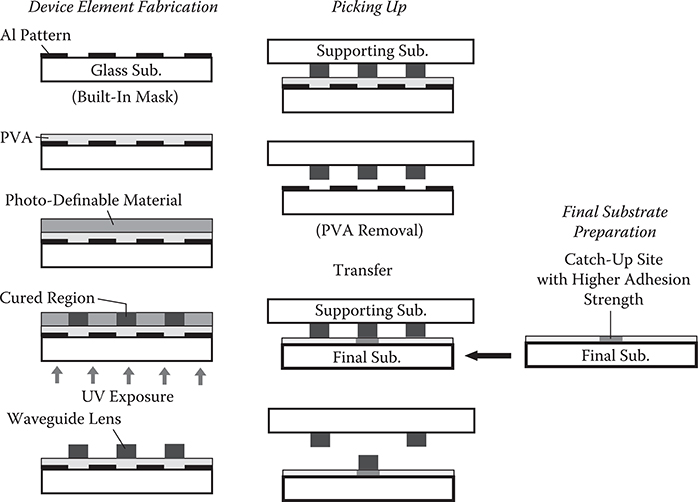
FIGURE 7.62 SORT process for polymer waveguide lenses. From T. Yoshimura, D. Tamaki, S. Kawamura, Y. Arai, and K. Asama, “A device transfer process ‘selectively occupied repeated transfer (SORT)’ for resource-saving integration of polymer micro optics fabricated by ‘built-in mask’ method,” IEEE Trans. Comp., Packag. Technol. 27, 468–471 (2004).
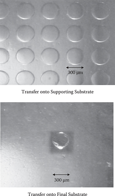
FIGURE 7.63 Photographs of a polymer waveguide lens array on the adhesive film of the supporting substrate (top), and a polymer waveguide lens transferred selectively onto the catch-up site of the final substrate (bottom). From T. Yoshimura, D. Tamaki, S. Kawamura, Y. Arai, and K. Asama, “A device transfer process ‘selectively occupied repeated transfer (SORT)’ for resource-saving integration of polymer micro optics fabricated by ‘built-in mask’ method,” IEEE Trans. Comp., Packag. Technol. 27, 468–471 (2004).
The SORT equipment was proposed by the author and was assembled by Suruga Seiki Co., Ltd. using components for fiber optics with positional accuracy of ~1 μm. Alignment between two substrates was achieved by optical stages, on which a lower substrate was set below the upper substrate holder.
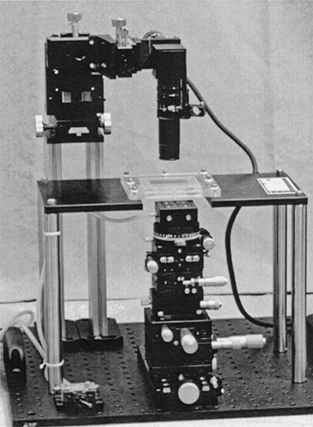
FIGURE 7.64 SORT equipment. From T. Yoshimura, T. Kofudo, T. Kashiwazako, K. Naito, K. Ogushi, and Y. Kitabayashi, “A material-saving optical waveguide fabrication process with selective transfers of cores,” Opt. Eng. 47, 014601-1-7 (2008).
7.5.3.2 SORT of Optical Waveguides
Figure 7.65(a) shows the concept of material-saving optical waveguide fabrication using SORT [41]. On a substrate, denoted by a picking-up substrate, cores for optical waveguides are placed in an array with high density. On final substrates, catch-up sites are formed. By attaching the picking-up substrate to a final substrate and detaching these, the cores are selectively transferred onto the final substrate to construct optical waveguides. In the case shown in Figure 7.65, since core pitch on the final substrate is six times larger than that on the picking-up substrate, one picking-up substrate can provide cores to six final substrates. This implies that six times the core materials are saved. For example, in chip-to-chip optical wiring with a core width of 40 μm and a core pitch of 250 μm, when cores are formed on the picking-up substrate with a 50-μm pitch and catch-up sites are arranged with a 250-μm pitch, it is expected that five times the waveguide materials can be saved.
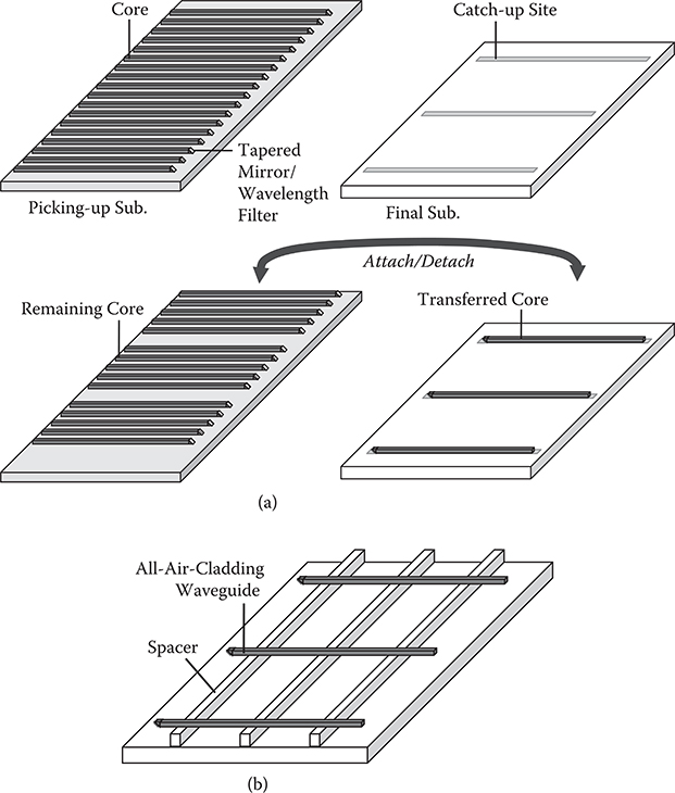
FIGURE 7.65 Concept of (a) material-saving optical waveguide fabrication using SORT, and (b) all-air-cladding waveguides for fine-pattern optical interconnects. From T. Yoshimura, T. Kofudo, T. Kashiwazako, K. Naito, K. Ogushi, and Y. Kitabayashi, “A material-saving optical waveguide fabrication process with selective transfers of cores,” Opt. Eng. 47, 014601-1-7 (2008).
In usual optical waveguides for chip-scale optical interconnects, devices such as vertical mirrors and wavelength filters with a metal/dielectric film coating on core end facets coexist. Complicated deposition/photolithography processes are involved in making these devices. The material-saving optical waveguide fabrication process shown in Figure 7.65 can also reduce the process steps for fabricating the coexisting devices by six times.
SORT is applicable to fabrication of all-air-cladding waveguides, as shown in Figure 7.65(b). For intrachip optical interconnects, fine-pattern optical circuits with light beam sizes confined to submicrons are necessary. To realize this, strong confinement of guided beams in cores is required by making the refractive index contrast between core and clad high. In optical waveguide–type light beam collecting films for photo-oltaic devices (which is described in Section 9.2), strong light beam confinement is also required. For these purposes, all-air-cladding waveguides, where all sides of the cores are surrounded by air, are promising. By transferring cores on spacers of final substrates, all-air-cladding waveguides may be obtained.
SORT of waveguide cores onto a glass substrate with catch-up sites was demonstrated as follows. A linear array of 3-cm-long cores with 32 × 32-μm2 cross-sections was formed with a 250-μm pitch on a built-in mask using a photo-definable material. The linear array was transferred to a picking-up substrate from the built-in mask. Meanwhile, catch-up sites were formed with a 500-μm pitch on a final substrate using the UV-curable-material-coated film. If devices are arranged in a linear array, direct transfers from the picking-up substrate to the final substrate are possible without the supporting substrate. So, by attaching/detaching of the two substrates, cores can be selectively transferred to the final substrate.
Figures 7.66(a) and (b) show the cores on the picking-up substrate and the final substrate after selective transfer. It can be seen that a core is transferred onto a catch-up site of the final substrate while a missing core site is found on the picking-up substrate. As Figure 7.66(c) shows, a guided beam of 650 nm in wavelength is clearly observed at the core edge.
These results confirm that SORT can be applied to transfer/integration of micro-scale optical circuits, including all-air-cladding waveguides.
FIGURE 7.66 Photographs of cores after selective transfer (a) on the picking-up substrate and (b) on the final substrate. (c) A guided beam in an optical waveguide with a transferred core. From T. Yoshimura, T. Kofudo, T. Kashiwazako, K. Naito, K. Ogushi, and Y. Kitabayashi, “A material-saving optical waveguide fabrication process with selective transfers of cores,” Opt. Eng. 47, 014601-1-7 (2008).

FIGURE 7.67 Duplication process of optical waveguide films with vertical mirrors using the built-in mask method. From T. Yoshimura, M. Miyazaki, Y. Miyamoto, N. Shimoda, A. Hori, and K. Asama, “Three-dimensional optical circuits consisting of waveguide films and optical Z-connections,” J. Lightwave Technol. 24, 4345–4352 (2006).
7.6 Optical Waveguide Films with Vertical Mirrors and 3-D Optical Circuits
One of the important elements for thin-film photonic device integration is OE films of optical waveguides with vertical mirrors. The OE films enable 3-D optical systems such as optical interconnect, optical switching, and solar energy conversion systems. In the present section, optical waveguide films with vertical mirrors duplicated by the built-in mask method and 3-D optical circuits constructed by stacking optical waveguide films are described.
7.6.1 OPTICAL WAVEGUIDE FILMS WITH VERTICAL MIRRORS
Figure 7.67 shows a duplication process of optical waveguide films with vertical mirrors using the built-in mask method [24,26,42]. On a glass substrate, Al film was deposited with patterns of cores to make a built-in mask. After a PVA removable layer and an under-cladding layer were successively formed on the mask, a 32-μm thick core layer was coated. For the under-cladding layer and the core, acrylic photo-definable polymers developed by JSR Corporation were used (OPSTAR PJ3045 for the under-cladding layer and OPSTAR PJ3001 for the core) [32]. The core layer was selectively exposed to a tilted UV light with a 45° incident angle through a prism put on the back of the built-in mask. By this process, cured structures with beveled walls with 45° slopes were constructed at the waveguide core ends, providing waveguide end facets for 45° mirrors. Vertical UV exposure was also carried out with a mask that covers the beveled wall regions to construct planar waveguide cores. The energy density of UV exposure using a high-pressure mercury lamp was ~1 J/cm2. By developing, core formation was completed. Finally, the removable layer was removed in water to obtain an optical waveguide film with 45° mirrors. The refractive index of the under-cladding layer is 1.56 and that of the core is 1.58 [32].
FIGURE 7.68 A photograph of an optical waveguide film with a vertical mirror duplicated by the built-in mask method, a tilted exposure setup, and NFP and FFP of a reflected beam from a vertical mirror.
Figure 7.68 shows a photograph of an optical waveguide film with a vertical mirror duplicated by the built-in mask method. Nominal core width is 32 μm. The waveguide end facet for a vertical mirror can be observed at the right edge of the core. Figure 7.68 also shows an example of a tilted exposure setup, and an near-field pattern (NFP) and an FFP of a reflected beam from a vertical mirror.
7.6.2 3-D OPTICAL CIRCUITS
Figure 7.69 shows two types of 3-D optical circuits for demonstration [26]. Type 1 is a stacked waveguide film with 45° mirrors. Two optical waveguide films (Films A and B) are stacked by contacting their under-cladding layers. No over-cladding layer is coated, meaning that the films have air-cladding waveguides. A probe beam is introduced at the Input in Film A. The beam is transferred into Film B through the Optical Z-Connection to reach the Output in Film B.
FIGURE 7.69 Schematic illustration of two types of 3-D optical circuits for demonstrations. From T. Yoshimura, M. Miyazaki, Y. Miyamoto, N. Shimoda, A. Hori, and K. Asama, “Three-dimensional optical circuits consisting of waveguide films and optical Z-connections,” J. Lightwave Technol. 24, 4345–4352 (2006).
Type 2 is a waveguide film with vertical waveguides. A vertical waveguide is constructed above a 45° mirror in an optical waveguide film using SOLNET. When a write beam is introduced at the Input, it is reflected into the PRI layer of a photo-polymer to grow a vertical waveguide at the Optical Z-Connection. The vertical waveguide confines a reflected probe beam to guide it efficiently to the Output at the PRI layer surface.
7.6.2.1 Type 1: Stacked Waveguide Films with 45° Mirrors
In Figure 7.70 a fabrication and measurement system for 3-D optical circuits consisting of stacked waveguide films is shown [26]. Film B put on an alignment stage was stacked on Film A with adjusting the positions of the 45° mirrors in Films A and B to construct the Optical Z-Connection. A single mode (SM) optical fiber for 1.3 μm was connected to the Input of a core in Film A by butt joint. A probe beam was introduced at the Input and propagated to the Output in Film B through the Optical Z-Connection.
Figure 7.71 shows the propagation of a 650-nm-wavelength probe beam in Films A and B. Before alignment, since the 45° mirror in Film B is not located above the 45° mirror in Film A, the probe beam reflected by the 45° mirror in Film A propagates through under-cladding layers to reach a camera set above the 45° mirror. After alignment, as shown in Figure 7.72, the two 45° mirrors are correctly aligned to form the Optical Z-Connection. The reflected probe beam can be transmitted into Film B through the Optical Z-Connection to reach the Output. A ~30 × 30 μm2 NFP is observed at the Output. Thus, 3-D optical wiring operation in the 3-D optical circuit is demonstrated successfully.
FIGURE 7.70 Fabrication/measurement system for 3-D optical circuits consisting of stacked waveguide films. From T. Yoshimura, M. Miyazaki, Y. Miyamoto, N. Shimoda, A. Hori, and K. Asama, “Three-dimensional optical circuits consisting of waveguide films and optical Z-connections,” J. Lightwave Technol. 24, 4345–4352 (2006).
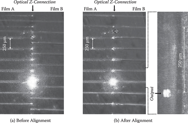
FIGURE 7.71 Probe beam propagation in the 3-D optical circuit with stacked waveguide films. From T. Yoshimura, M. Miyazaki, Y. Miyamoto, N. Shimoda, A. Hori, and K. Asama, “Three-dimensional optical circuits consisting of waveguide films and optical Z-connections,” J. Lightwave Technol. 24, 4345–4352 (2006).
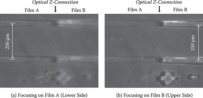
FIGURE 7.72 Photographs of the Optical Z-Connection part. From T. Yoshimura, M. Miyazaki, Y. Miyamoto, N. Shimoda, A. Hori, and K. Asama, “Three-dimensional optical circuits consisting of waveguide films and optical Z-connections,” J. Lightwave Technol. 24, 4345–4352 (2006).
7.6.2.2 Type 2: Waveguide Films with Vertical Waveguides of SOLNET
As one of the ways for loss reduction at the Optical Z-Connection, implementation of a 3-D optical circuit consisting of vertical waveguides on an optical waveguide film is effective. The fabrication/measurement system is shown in Figure 7.73 [26]. On the back of an under-cladding layer in an optical waveguide film, a ~500-μm-thick PRI layer of photo-polymer was coated. The photo-polymer developed by JSR Corporation consists of acrylic/epoxy components [32].
A write beam of 405-nm blue laser diode (LD) was introduced from a SM optical fiber at the Input of the optical waveguide film with power of ~100 μW or less. The propagated write beam was reflected to the surface-normal direction by a 45° mirror. The write beam passed through the under-cladding layer and was injected into the PRI layer. Then, a vertical waveguide of SOLNET was formed in the PRI layer. A probe beam of 650-nm wavelength was introduced at the Input of the optical waveguide film. The beam was guided in the vertical waveguide at the Optical Z-Connection to reach the Output at the PRI layer surface of the SOLNET.
In Figure 7.74(a), SOLNET grown vertically on the under-cladding layer is shown. It is found that the vertical waveguide is constructed in the photo-polymer layer above the 45° mirror. As shown in Figure 7.74(b), a near-field pattern of the probe beam with an area of ~30 × 30 μm2, which is approximately the same as the core size of the optical waveguide film, is observed at the Output. These results demonstrate the 3-D optical wiring capability of the vertical waveguide of SOLNET.
It should be noted that SOLNET was formed by a write beam from the under-cladding layer, which is a free space with no beam-confining structures. In other words, SOLNET can be formed even when some spacers are inserted between 45° mirrors and PRI layers. An experimental measurement of SOLNET formed between two optical fibers suggests that loss in SOLNET is around 0.7 dB.
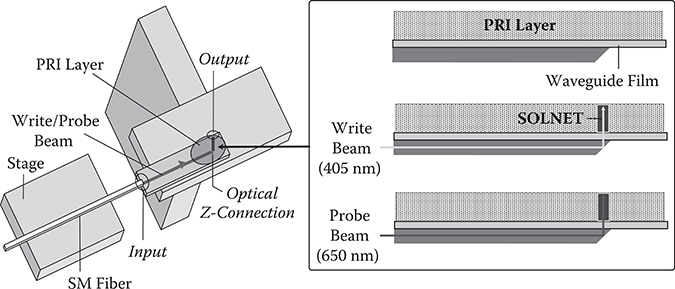
FIGURE 7.73 Fabrication/measurement system for 3-D optical circuits of waveguide films with vertical waveguides of SOLNET. From T. Yoshimura, M. Miyazaki, Y. Miyamoto, N. Shimoda, A. Hori, and K. Asama, “Three-dimensional optical circuits consisting of waveguide films and optical Z-connections,” J. Lightwave Technol. 24, 4345–4352 (2006).
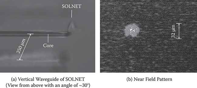
FIGURE 7.74 (a) Vertical waveguide of SOLNET grown above the 45° mirror. (b) NFP of the probe beam guided in the vertical waveguide. From T. Yoshimura, M. Miyazaki, Y. Miyamoto, N. Shimoda, A. Hori, and K. Asama, “Three-dimensional optical circuits consisting of waveguide films and optical Z-connections,” J. Lightwave Technol. 24, 4345–4352 (2006).
By combining 3-D optical circuits of Type 1 and 2, SOLNET can be inserted between two 45° mirrors. By connecting two waveguide films with vertical waveguides of SOLNET, light beams may be guided from one 45° mirror to the other with strong confinement, reducing the leakage of the light beams at the Optical Z-Connection.
References
1. K. D. Singer, M. G. Kuzyk, W. R. Holland, J. E. Sohn, S. J. Lalama, R. B. Comizzoli, H. E. Katz, and M. L. Schilling, “Electro-optic phase modulation and optical second-harmonic generation in corona-poled polymer films,” Appl. Phys. Lett. 53, 1800–1802 (1988).
2. B. F. Levine, C. G. Bethea, C. D. Thurmond, R. T. Rynth, and J. L. Bernstein, “An organic crystal with an exceptionally large optical second-harmonic coefficient: 2-methyl-4-nitroaniline,” J. Appl. Phys. 50, 2523–2527 (1979).
3. G. F. Lipscomb, A. F. Garito, and R. S. Narang, “An exceptionally large electro-optic effect in the organic solid MNA,” J. Chem. Phys. 75, 1509–1516 (1981).
4. T. Yoshimura, “Enhancing second-order nonlinear optical properties by controlling the wave function in one-dimensional conjugated molecules,” Phys. Rev. B40, 6292–6298 (1989).
5. T. Yoshimura, S. Tatsuura, and W. Sotoyama, “Quantum well formation in one-dimensional polymer films by molecular layer deposition and chemical vapor deposition,” Mat. Res. Soc. Symp. Proc. 247, 829–834 (1992).
6. T. Yoshimura, “Characterization of the EO effect in styrylpyridinium cyanine dye thin-film crystals by an ac modulation method,” J. Appl. Phys. 62, 2028–2032 (1987).
7. G. R. Meredith, “Design and characterization of molecular and polymeric nonlinear optical materials: Successes and pitfalls,” in Nonlinear optical properties of organic and polymeric materials (Ed. D. J. Williams), 27–56, American Chemical Society, Washington, DC (1983).
8. J. S. Wei and W. D. Westwood, “A new method for determining thin-film refractive index and thickness using guided optical waves,” Appl. Phys. Lett. 32, 819–821 (1978).
9. Y. Kubota and T. Yoshimura, “Endothermic reaction aided crystal growth of 2-methyl-4-nitroaniline and their electro-optic properties,” Appl. Phys. Lett. 53, 2579–2580 (1988).
10. T. Yoshimura and Y. Kubota, “Pockels effect in organic thin films,” Springer Proceedings in Physics 36, Nonlinear Optics of Organics and Semiconductors, Springer-Verlag Berlin, Heidelberg, 222–226 (1989).
11. T. Yoshimura, S. Tatsuura, and W. Sotoyama, “Organic electro-optic materials and their applications,” Oyo Buturi 61, 38–42 (1992) [in Japanese].
12. W. Sotoyama, S. Tatsuura, and T. Yoshimura, “Electro-optic side-chain polyimide system with large optical nonlinearity and high thermal stability,” Appl. Phys. Lett. 64, 2197–2199 (1994).
13. C. C. Teng and H. T. Man, “Simple reflection technique for measuring the electro-optic coefficient of poled polymers,” Appl. Phys. Lett. 56, 1734–1736 (1990).
14. W. Sotoyama, S. Tatsuura, K. Motoyoshi, and T. Yoshimura, “Directional-coupled optical switch between stacked waveguide layers using electro-optic polymer,” Jpn. J. Appl. Phys. 31, L1180–L1181 (1992).
15. W. Sotoyama, S. Tatsuura, and T. Yoshimura, “Fabrication techniques for electro-optic polymer waveguides,” The Review of Laser Engineering, 21, 1125–1133 (1993) [in Japanese].
16. S. Tatsuura, W. Sotoyama, and T. Yoshimura, “Epoxy-amine polymer waveguide containing nonlinear optical molecules fabricated by chemical vapor deposition,” Appl. Phys. Lett. 60, 1158–1160 (1992).
17. S. Tatsuura, W. Sotoyama, and T. Yoshimura, “Electro-optic polymer waveguide fabricated using electric-field-assisted chemical vapor deposition,” Appl. Phys. Lett. 60, 1661–1663 (1992).
18. S. Tatsuura, W. Sotoyama, K. Motoyoshi, A. Matsuura, T. Hayano, and T. Yoshimura, “Polyazomethine conjugated polymer film with second order nonlinear optical properties fabricated by electric-field-assisted chemical vapor deposition,” Appl. Phys. Lett. 62, 2182–2184 (1993).
19. K. Matsumoto and T. Yoshimura, “Electro-optic waveguides with conjugated polymer films fabricated by the carrier-gas-type organic CVD for chip-scale optical interconnects,” Proc. SPIE 6899, from Photonics West 2008, San Jose, California, 98990E- 1-9 (2008).
20. H. Rong, R. Jones, A. Liu, O. Cohen, Y.H. Kuo, and M. Paniccia, “Silicon-based laser, amplifier, and wavelength converter for optoelectronic integration,” Proc. SPIE 6125, 612505-1-13 (2006).
21. R. M. Kubacki, “Micro-optic enhancement and fabrication through variable in-plane index of refraction (VIPIR) engineered silicon nanocomposite technology,” Proc. SPIE 5347, 233–246 (2004).
22. S. Ono, T. Yoshimura, T. Sato, and J. Oshima, “Fabrication and evaluation of nano-scale optical circuits using sol-gel materials with photo-induced refractive index variation characteristics,” J. Lightwave Technol. 27, 1229–1235 (2009).
23. A. Bhatnagar, S. Latif, C. Debaes, and D. A. B. Miller, “Pump-probe measurements of CMOS detector rise time in the blue,” J. Lightwave Technol. 22, 2213–2217 (2004).
24. T. Yoshimura, T. Inoguchi, T. Yamamoto, S. Moriya, Y. Teramoto, Y. Arai, T. Namiki, and K. Asama, “Self-organized lightwave network based on waveguide films for three-dimensional optical wiring within boxes,” J. Lightwave Technol. 22, 2091–2100 (2004).
25. T. Yoshimura, M. Miyazaki, Y. Miyamoto, N. Shimoda, A. Hori, and K. Asama, “Three-dimensional optical circuits consisting of waveguide films and optical Z-connections,” J. Lightwave Technol. 24, 4345–4352 (2006).
26. E. Cassan, S. Laval, S. Lardenois, and A. Koster, “On-chip optical interconnects with compact and low-loss light distribution in silicon-on-insulator rib waveguides,” IEEE J. Select. Topics Quantum Electron. 9, 460–464 (2003).
27. T. Yoshimura, J. Roman, Y. Takahashi, W. V. Wang, M. Inao, T. Ishitsuka, K. Tsukamoto, K. Motoyoshi, and W. Sotoyama, “Self-organizing waveguide coupling method ‘SOLNET’ and its application to film optical circuit substrates,” Proc. 50th Electronic Components & Technology Conference (ECTC), Las Vegas, Nevada, 962–969 (2000).
28. T. Yoshimura, J. Roman, Y. Takahashi, W. V. Wang, M. Inao, T. Ishitsuka, K. Tsukamoto, K. Motoyoshi, and W. Sotoyama, “Self-organizing lightwave network (SOLNET) and its application to film optical circuit substrates,” IEEE Trans. Comp., Packag. Technol. 24, 500–509 (2001).
29. T. Yoshimura, W. Sotoyama, K. Motoyoshi, T. Ishitsuka, K. Tsukamoto, S. Tatsuura, H. Soda, and T. Yamamoto, Method of producing optical waveguide system, optical device and optical coupler employing the same, optical network and optical circuit board, U.S. Patent 6,081,632 (2000).
30. T. Yoshimura, M. Ojima, Y. Arai, and K. Asama, “Three-dimensional self-organized micro optoelectronic systems for board-level reconfigurable optical interconnects: performance modeling and simulation,” IEEE J. Select. Topics in Quantum Electron. 9, 492–511 (2003).
31. T. Yoshimura, A. Hori, Y. Yoshida, Y. Arai, H. Kurokawa, T. Namiki, and K. Asama, “Coupling efficiencies in reflective self-organized lightwave network (R-SOLNET) simulated by the beam propagation method,” IEEE Photon. Technol. Lett. 17, 1653–1655 (2005).
32. F. Huang, H. Takase, Y. Eriyama, and T. Ukachi, “Optical fiber interconnection by using self-written waveguides,” Proc. 9th Int. Conf. Rad. Tech. Asia, Japan, 637–639 (2003).
33. T. Yoshimura and H. Kaburagi, “Self-organization of optical waveguides between mis-aligned devices induced by write-beam reflection,” Appl. Phys. Express 1, 062007-1-3 (2008).
34. H. Kaburagi and T. Yoshimura, “Simulation of micro/nano-scale self-organized light-wave network (SOLNET) using the finite difference time domain method,” Opt. Commun. 281, 4019–4022 (2008).
35. T. Yoshimura, J. Roman, Y. Takahashi, M. Lee, B. Chou, S. Beilin, W. Wang, and M. Inao, “Optoelectronic scalable substrates based on film/Z-connection and its application to film optical link module (FOLM),” Proc. SPIE 3952, from Photonics West 2000, San Jose, California, 202–213 (2000).
36. T. Yoshimura, K. Kumai, T. Mikawa, O. Ibaragi, and M. Bonkohara, “Photolithographic packaging with selectively occupied repeated transfer (PL-Pack with SORT) for scalable optical link multi-chip-module (S-FOLM),” IEEE Trans. Electron. Packag. Manufact. 25, 19–25 (2002).
37. N. M. Jokerst, M. A. Brooke, S. Cho, S. Wilkinson, M. Vrazel, S. Fike, J. Tabler, Y. J. Joo, S. Seo, D. S. Wils, and A. Brown, “The heterogeneous integration of optical interconnections into integrated microsystems,” IEEE J. Select. Topics in Quantum Electron. 9, 350–360 (2003).
38. E. Yablonovitch, T. Gmitter, J.P. Harbison, and R. Bhat, “Extreme sensitivity in the lift-off of epitaxial GaAs films,” Appl. Phys. Lett. 51, 2222–2224 (1987).
39. C. Stirk, Q. Liu, and M. Ball, “Manufacturing cost analysis of integrated photonic packages,” Proc. SPIE 3631, 224–233 (1999).
40. T. Yoshimura, D. Tamaki, S. Kawamura, Y. Arai, and K. Asama, “A device transfer process “Selectively occupied repeated transfer (SORT)” for resource-saving integration of polymer micro optics fabricated by “built-in mask” method,” IEEE Trans. Comp., Packag. Technol. 27, 468–471 (2004).
41. T. Yoshimura, T. Kofudo, T. Kashiwazako, K. Naito, K. Ogushi, and Y. Kitabayashi, “A material-saving optical waveguide fabrication process with selective transfers of cores,” Opt. Eng. 47, 014601- 1-7 (2008).
42. T. Inoguchi, S. Moriya, T. Yamamoto, Y. Arai, T. Yoshimura, and K. Asama, “Film waveguides with micro mirrors for three-dimensional optical circuits fabricated by the built-in mask method,” J. Electronics Jisso 8, 237–242, 2005 [in Japanese].