
2 Atomic/Molecular Assembling Technologies
In Table 2.1, various kinds of atomic/molecular assembling technologies are summarized. The scanning tunneling microscope (STM) is applicable to both atomic and molecular assembling. While sputtering, molecular beam epitaxy (MBE), chemical vapor deposition (CVD), atomic layer apitaxy (ALE), and atomic layer deposition (ALD) are used for atomic assembling, vacuum deposition polymerization and molecular layer deposition (MLD) are used for molecular assembling. In the case of molecular assembling, since the growth is three-dimensional, wire orientations should be controlled. Therefore, selective wire growth has been added in the table.
This chapter begins with an explanation of the similarity of electronic waves to light waves, which is useful to understand the behavior of electron wavefunctions. Then, examples of tailored materials with atomic/molecular assembling by STM, MBE, ALD, plasma CVD, sputtering, and vacuum deposition polymerization are presented. MLD, which is the main theme of the present book, will be precisely described in Chapter 3 and Chapter 4, together with selective wire growth.
2.1 Similarity of Electronic Waves to Light Waves
In order to easily understand the behavior of electron wavefunctions, the similarity of electronic waves to light waves is briefly considered in this section. Figure 2.1(a) shows an analogy between the electron confinement and the photon confinement. The wavefunction of electron ψ and the electric field of light waves E are determined by the following wave equations.
Here, m, V, and E are mass, potential energy, and total energy of an electron, respectively. ħ is the Plank constant divided by 2π; n is the refractive index, and k0 is the wavenumber in vacuum. These equations can be written as follows:
TABLE 2.1
Atomic/Molecular Assembling Technologies
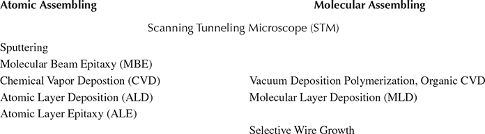
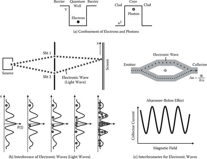
FIGURE 2.1 Similarity of electronic waves to light waves.
Comparing these two equations, it is found that the following relationships exist.
It is known that an electron tends to be confined in a region with lower potential energy as shown in Figure 2.1(a). The above-mentioned relationships indicate that –V(x) corresponds to n2(x). This suggests that a photon tends to be confined in a region with a larger refractive index. Therefore, by forming lower-potential-energy regions in a media with designated patterns, waveguides for electronic waves can be constructed. Similarly, by forming higher-refractive-index regions, waveguides for light waves can be constructed.
As is well known, light waves passing through two slits make an interference pattern of light intensity I on a screen. Similarly, electronic waves passing through two slits make an interference pattern of probability P = ψ*ψ that an electron will arrive at x. The interference pattern is schematically illustrated in Figure 2.1(b). Many electrons are attracted to places where P = ψ*ψ is large, making many spots on the screen.
Figure 2.1(c) shows an interferometer for electronic waves [1]. Waveguides are formed in a shape of the Mach-Zehnder interferometer. Electronic waves are emitted from the emitter. The waves are divided into two paths of the upper arm and the lower arm, and come together in the output waveguide to reach the collector. When magnetic flux exists in the area between the two arms, a phase difference is induced between the two paths via the Aharonov-Bohm effect. Then, the collector current oscillates as a function of the magnetic field due to interference of the electronic waves from the upper arm and the lower arm. Exactly the same phenomena are observed in the Mach-Zehnder interferometer of optical waveguides.
As described, most of the behavior of the electronic waves of ψ can be understood by analogy with the behavior of the light waves of E.
2.2 Scanning Tunneling Microscopy (STM)
2.2.1 ATOMIC MANIPULATION
Eigler and Schweizer developed an atomic manipulation process that enables atoms to slide across a surface to definite positions as shown in Figure 2.2 [2]. The process utilizes atomic force between the atoms and atoms on the edge of the STM tip.
Figure 2.3 shows the dependence of potential energy on the distance between atoms (molecules). Potential energy arising from Pauli’s exclusion principle is extremely large in short distance regions, and it decreases rapidly with distance. The potential energy arising from van der Waals’ force, on the other hand, decreases gradually with the distance as compared with the case of Pauli’s exclusion principle. As a result, the total potential curve has a minimum. Force F is given by
using potential energy function V. Then, attractive atomic force arises between atoms (molecules) for distances longer than the minimum point because the slope of the potential curve is positive there. For distances shorter than the minimum point, since the slope of the potential curve is negative, repulsive atomic force arises, giving rise to a stable distance at the minimum point.
Using the atomic force between an atom on a substrate surface and an atom on a tip, the atom on the surface can be carried by the tip as shown in Figure 2.2. When the tip is pointing down to the atom and is placed at a distance with a positive potential curve slope, attractive force arises between the atom and the tip. By moving the tip, the atom slides on the surface. After pulling the tip up vertically, the force between the atom and the tip vanishes.
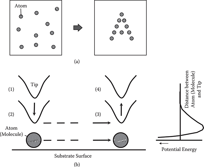
FIGURE 2.2 Schematic illustration of sliding atoms across a surface to definite positions to draw an image, and (b) procedure for sliding atoms by STM.
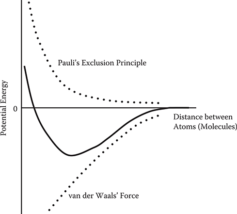
FIGURE 2.3 Dependence of potential energy on distance between atoms (molecules).
2.2.2 Detection of Wavefunctions
Figure 2.4 shows the tunneling process in STM. When a tip is put on a sample surface with a small gap of 1-nm scale, electron wavefunctions penetrate through the gap by the tunneling effect. The tunneling probability is proportional to , where, d, m, and E are, respectively, gap length, electron mass, and electron energy. V is the barrier height at the gap and ħ is Plank’s constant divided by 2π. When the tip bias is close to the energy of an electronic state in the sample, a tunnel current increases. When the tip bias is far from the energy of the state, the tunnel current decreases. Therefore, in constant current mode, the distance between the tip and the sample surface becomes large when an electronic state with energy close to the tip bias exists in the sample, and it becomes small when the state does not exist. Using this property of STM, wavefunction shapes can be detected by STM as shown in Figure 2.5. In the figure, ψ represents the wavefunction of the state with energy close to the tip bias. The tip goes away from the surface in the region with large ψ, and gets close to the surface in the region with small ψ, enabling us to draw the shape of ψ*ψ by the up–down movement of the tip.
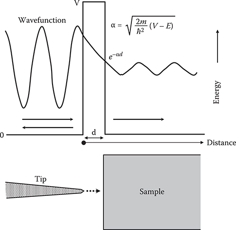
FIGURE 2.4 Tunneling process in STM.
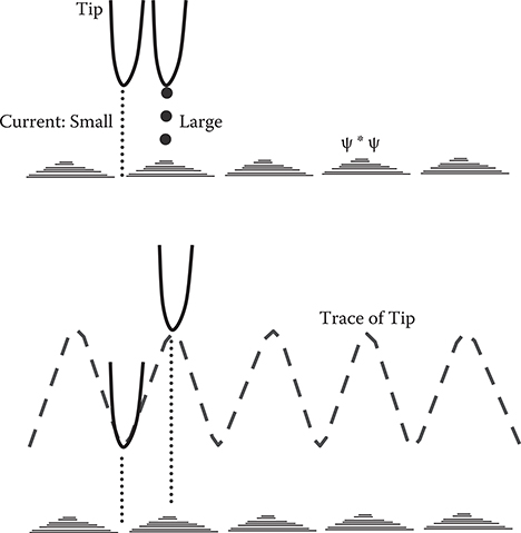
FIGURE 2.5 Detection of wavefunction shapes by STM.
2.2.3 QUANTUM CORRAL and QUANTUM MIRAGE
Figure 2.6 shows an experiment of electron confinement in a quantum corral, which was reported by Eigler et al. [3]. By STM, 48 Fe atoms are positioned into a ring with a 7.13-nm radius on the Cu surface to construct a quantum corral. Due to the quantum confinement effect by the corral, standing waves of ψ for electrons confined in the corral appear. The shape of ψ*ψ can be monitored by STM as schematically shown in Figure 2.6. Eigler et al. also succeeded to generate a quantum mirage in an elliptical quantum corral [4]. As Figure 2.7 shows, they put a Co atom at one focus of the corral, and observed a quantum mirage projected around another focus. Due to interference of wavefunctions of electrons scattered by the Co atom, the electronic structures surrounding the Co atom are regenerated near another focus just like the interference of light on an elliptical mirror surface.
2.3 Molecular Beam Epitaxy (MBE)
2.3.1 GROWTH MECHANISM OF MBE
MBE is an important growth technique for inorganic thin films on flat substrate surfaces. Since MBE has thickness controllability of mono-atomic-layer scales, it has greatly contributed to the development of various kinds of functional devices by the semiconductor industry. The superlattice developed by Esaki and Tsu [5] is the distinguished innovation achieved by MBE. Transistors, light modulators, laser diodes (LDs) utilizing ultrathin films and quantum wells were also developed by MBE.
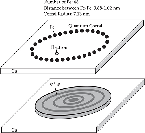
FIGURE 2.6 Electron confinement in a quantum corral.
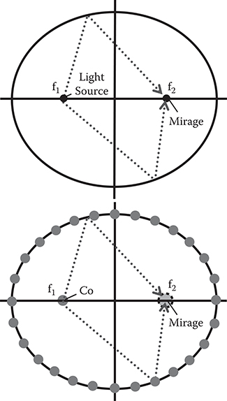
FIGURE 2.7 Quantum mirage.
Figure 2.8 shows the growth mechanism of MBE. Incident atoms on the surface behave as a potential curve shown at the bottom of the figure. The curve has two minimum points. The shallow minimum causes physical adsorption arising from a weak force such as van der Waals’ force without chemical bonds to the surface. This corresponds to the minimum shown in Figure 2.3. The deep minimum causes chemical adsorption with chemical bonds on the surface. Incident atoms, initially, are weakly adsorbed on the surface as physical adsorption. After the atoms migrate on the surface for a while, the adsorption state changes from physical adsorption to chemical adsorption to fix the atoms at specific sites. Next, incident atoms migrating on the surface reach the previous atoms fixed on the surface, and are chemically adsorbed to form growth centers. A monolayer is grown from the growth centers to cover the entire surface. This procedure is repeated to grow thin films.
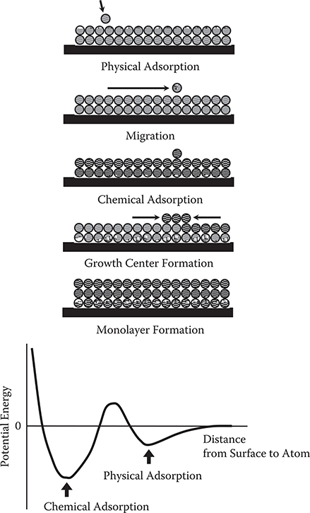
FIGURE 2.8 Growth mechanism of MBE.
2.3.2 HIGH-ELECTRON-MOBILITY TRANSISTORS
One of the functional devices fabricated by MBE is the high-electron-mobility transistor (HEMT) [6], which is basically a field-effect transistor. Figure 2.9 shows an example of the structure. In the Al1−xGaxAs layer that has a wide band gap, Si is doped as a dopant for donors. Electrons from the donors are transferred to an adjacent nondoped GaAs layer to provide two-dimensional electron gases that form channels. Thus, in HEMT, the doped layer is separated from the channel layer to reduce scattering of electrons in the channel, increasing carrier mobility.
2.3.3 MULTIPLE QUANTUM WELL LIGHT MODULATORS
Another functional device is the light modulator, which consists of multiple quantum wells [7] that can be fabricated by MBE. Figure 2.10(a) shows schematic illustrations of band diagrams and electron orbitals in bulk and quantum well structures. When an electron is excited by light absorption, an electron-hole pair, an exciton, is generated. Due to attractive force between an electron and a hole, the energy level of the exciton is located below the conduction band edge. The difference in energy between the band edge and the exciton level gives binding energy of the exciton, denoted by EB. In quantum wells, excited electrons are confined in narrow spaces; then, deformation in electron orbitals is caused, making the average distance between electrons and holes smaller compared with the bulk case. Consequently, in quantum wells, the binding energy increases, and the dissociation probability of the exciton decreases to increase the life time, τ, of the exciton.
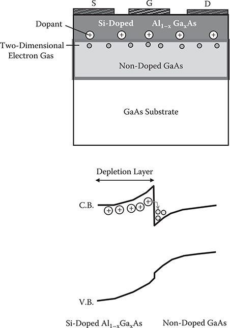
FIGURE 2.9 HEMT.
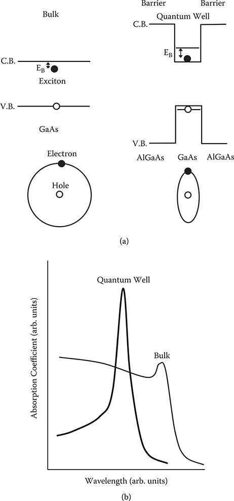
FIGURE 2.10 (a) Schematic illustrations of band diagrams and electron orbitals in bulk and quantum well structures. (b) Sharpening of exciton absorption bands by the quantum confinement in quantum wells.
The uncertainty principle tells us that, with an increase in τ, the uncertainty of energy decreases, that is, the width of exciton absorption bands becomes narrow. Thus, as shown in Figure 2.10(b), sharpening of exciton absorption bands is realized in quantum wells. The sharpening is favorable for light modulation and will be described later. It should be noted that a blue shift of the absorption band occurs in quantum wells. This is attributed to an increase in the energy gap due to the electron (hole) confinement effect, which is shown in Figure 2.10(a).
When electric fields are applied to the quantum well, a slope appears in the energy bands as shown in Figure 2.11(a). Then, energy levels for electrons decrease while those for holes increase, resulting in a red shift of the absorption band as shown in Figure 2.11(b). The absorption band shift enables light modulation. With the same amount of wavelength shift of the absorption bands, the sharper the absorption bands become, and the larger the modulation contrast becomes.
In addition, by applying electric fields to the quantum well, the electron wavefunction and the hole wavefunction are moved in opposite directions to reduce wavefunction overlap between the ground state and the excited state. This causes a decrease in transition probability for the electron excitation, inducing a decrease in absorption peak height.
2.3.4 RELATIONSHIPS TO OTHER GROWTH TECHNIQUES
MBE is also applied to fabrication of heterogeneous junctions with thin layers in laser diodes (LDs), superlattice devices, and quantum wires and dots with the assistance of surface treatment. One problem of MBE is lack of conformality. Ultrathin layers can be grown on flat surfaces, but cannot be grown on surfaces with rough structures, porous structures, or three-dimensional structures. Another problem is controllability. Even for flat surfaces, in order to control growth thicknesses with mono-atomic-layer accuracy, high-quality monitoring is required, such as electron diffraction measurements. One more problem is mass productivity. Film growth can be performed only on a limited number of substrates or on a limited area of substrates because MBE utilizes oriented molecular beams in vacuum. For mass production, metal-organic CVD (MOCVD) was developed. A more advanced growth technique is ALD, which has been received much attention recently. The details of ALD are covered in Section 2.4.
2.4 Atomic Layer Deposition (ALD)
ALD is an inorganic film growth method invented by Suntola [8]. In ALD, by introducing two kinds of molecules onto substrate surfaces alternately, ultrathin films are grown with mono-atomic layer steps.
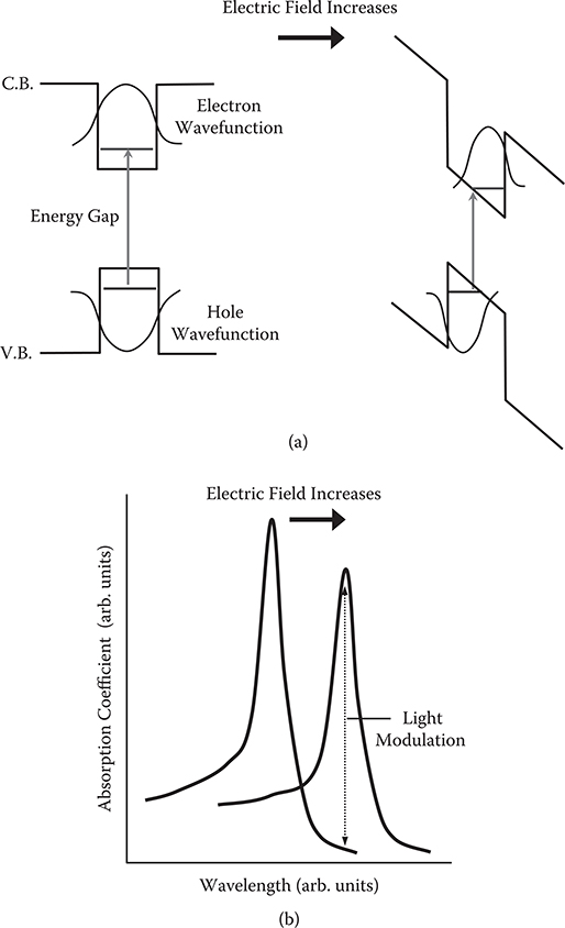
FIGURE 2.11 Effects of applied electric fields on (a) band diagrams of quantum well structures (b) absorption band shifts.
Figure 2.12 shows the ALD process for ZnS thin film growth. On a substrate surface, ZnCl2 is introduced to form a layer that covers the surface. (1) After removing ZnCl2, H2S is introduced on the surface. (2) ZnCl2 and H2S react to form an S layer on a Zn surface. (3) Once the surface is covered with S, H2S re-evaporates from the surface since no chemical reaction occurs between H2S and S. Thus, the film growth is terminated. This is called the self-limiting effect. (4) Next, after H2S removal, ZnCl2 is introduced again. (5) Due to the self-limiting effect, an exact mono layer of ZnCl2 is formed on the surface. (6) By providing ZnCl2 and H2S alternately, a ZnS film is formed layer by layer.
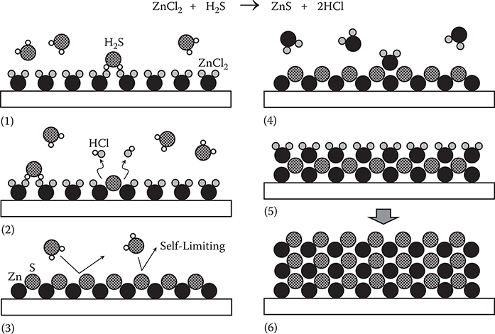
FIGURE 2.12 ALD process for ZnS thin film growth.
ALD was initially developed as atomic layer epitaxy (ALE) for inorganic thin-film AC electroluminescent (EL) devices. Recently ALE and ALD have received much attention for a wide range of applications.
The advantages and current applications of ALD are summarized in Table 2.2. The most outstanding feature of ALD is that it can deposit ultrathin conformal films on surfaces with arbitrary shapes, such as trenches, cylinders, paper, fibers, pours and rough structures, and so on. Typical materials deposited by ALD are ZnS, ZnO, SiO2, HfO2, ZrO2, Al2O3, TiO2, and various types of metals. ALD is applied to ultra-thin/high-k gate insulators of large-scale integrated circuits (LSIs) and capacitors with ultralarge capacitance. It is also applied to solar cells, fuel cells, catalysts, optical devices such as gratings, thin-film transistors, EL devices, and as a surface treatment for various materials including surfaces with three-dimensional structures, porous materials, paper, and fibers.
Figure 2.13 shows examples of the deposition of ultra-conformal films in trenches with high aspect ratios by ALD [9]. The upper picture represents a filling-hole process by ALD. The lower illustration represents ultrathin multilayer formation on a trench surface. This enables capacitors with large capacitance, because the effective area of the capacitors increases. The same structure can be applied to electrostatic or electrochemical batteries. Fuel cells with an ultrathin solid electrolyte, which decreases series electrical resistance, were also reported [10].
TABLE 2.2
Advantages and Current Applications of ALD
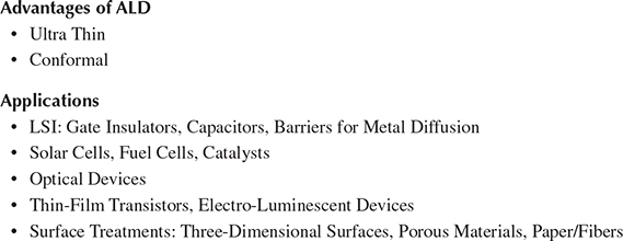
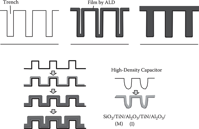
FIGURE 2.13 Examples of deposition of ultra-conformal films in trenches with a high aspect ratio by ALD.
Figure 2.14 shows examples of nano-scale structure fabrication using ALD [11]. On nano-scale cylindrical templates, thin films are deposited by ALD. By removing the templates, nanotubes and vertical walls are obtained. Figure 2.15 shows metal-oxide semiconductor field-effect transistor (MOSFET) with an ultrathin gate insulator layer deposited by ALD. When compared to the conventional deposition method, ALD reduces leakage currents drastically, indicating that conformality of the insulate layer is improved by ALD. ALD applications in other fields, such as hydrophobic surface treatment of cotton fibers and tissue papers, were demonstrated [12].
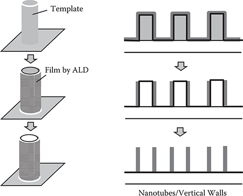
FIGURE 2.14 Examples of nano-scale structure fabrication using ALD.
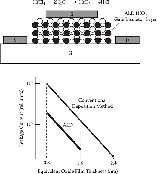
FIGURE 2.15 MOSFET with an ultrathin gate insulator layer deposited by ALD.
One drawback of ALD is low deposition rate, which is caused by gas switching duration. To resolve the problem, novel ALD equipment with improved deposition rates were proposed recently. Two examples are illustrated in Figure 2.16. One example uses rotating gas injectors, in which it takes only a few seconds for one evolution [9]. The other uses injector arrays [13]. Injectors for metal, oxidizer, and purge are arranged periodically. Substrates move through the injector arrays.
Expected future challenges of ALD are shown in Figures 2.17 and 2.18. By arranging more than three kinds of atoms by ALD, quantum wells and superlattices may easily be constructed, providing, for example, artificial nonlinear optical materials and electrochromic materials. Optical nonlinearity like the electro-optic (EO) effect of materials is determined by wavefunction shapes of electrons as described in Chapter 5. Thin film deposition with atomic layer steps enables us to optimize the wavefunction shapes by the arrangement of atoms. When electric fields are applied to the material, the wavefunction shape changes to induce a refractive index change. For electrochromic devices, the electron-donating layer, electron-accepting layer, and electron-blocking layer are stacked layer by layer. By electric fields, electrons are transferred from the electron-donating layer to the electron-accepting layer to induce polarization. Then, each layer changes to mixed valence states to induce coloration due to the intervalence transition, which is explained in Subsection 2.6.2.
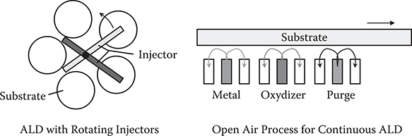
FIGURE 2.16 ALD equipment with high deposition rates.
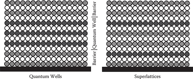
FIGURE 2.17 Proposed quantum wells and superlattices by ALD.
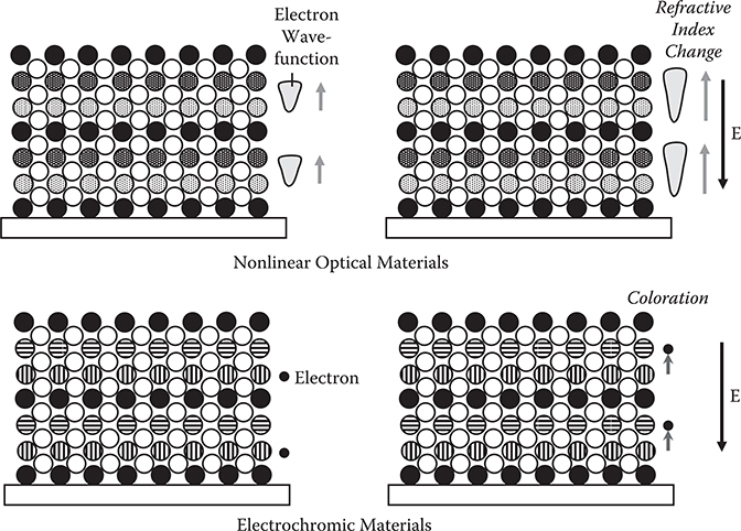
FIGURE 2.18 Proposed artificial nonlinear optical materials and electrochromic materials with quantum wells and superlattices by ALD.
2.5 Plasma Chemical Vapor Deposition (Plasma CVD)
For growth of amorphous materials such as a-Si:H, a-SiNx:H, and a-SiOx, plasma CVD is frequently used. Plasma CVD can perform precise composition modulation during film growth by controlling reactive gas composition, enabling fabrication of superlattices as MBE. In this section, as an example of material property control by atomic-level tailored structures, photocurrent enhancement induced by layer composition/thickness optimization in amorphous superlattices is described.
2.5.1 AMORPHOUS SUPERLATTICES
Amorphous superlattices [14] are grown by stacking ultrathin films with different composition sequentially. One of the interesting phenomena observed in amorphous superlattices is the transfer doping effect. The effect has been found in a-SiNx:H/a-Si:H superlattices [14, 15 and 16], and explained as electron transfer from states in the band gap of the a-SiNx:H layer or interface states to the a-Si:H layer. The electron transfer induces electron accumulation in the a-Si:H layer, giving rise to an increase in the in-plane conductivity by several orders of magnitude. Meanwhile, at an a-SiNx:H/a-Si:H interface, electron trapping by states in the band gap of the a-SiNx:H layer has also been observed. The electron trapping affects the threshold voltage of a-Si thin film transistors (TFTs) with a-SiNx:H gate insulators [17].
The transfer-doping and electron-trapping effects at the a-SiNx:H/a-Si:H interface depend strongly on the a-SiNx:H composition. This suggests that composition dependency of transfer-doping and electron-trapping effects is expected in a-SiNx:H/a-Si:H superlattices. Detailed investigation of these effects in amorphous superlattices is shown in Subsection 2.5.3 [18].
2.5.2 CHARACTERIZATION OF THE A-SINx:H/A-SI:H INTERFACE
Defects induced near the a-SiNx:H/a-Si:H interface may have an influence on the characteristics of amorphous superlattices consisting of a-SiNx:H/a-Si:H as well as the characteristics of a-Si TFTs with an a-SiNx:H gate insulator. Therefore, characterization of the near-interface properties is important to understanding the amorphous superlattices. Photoluminescence measurement is effective in detecting defects. By selecting suitable excitation energy, it is possible to obtain photoluminescence spectra of a particular region of a thin film.
In this subsection, investigation of the near-interface region in a-SiNx:H/a-Si:H layered structures by photoluminescence measurement is described to show how the near-interface properties of a-Si:H vary depending on the nitrogen content of a-SiNx:H [19]. The results are compared with the field effect mobility in a TFT, and are discussed in terms of the concentration of deep states induced in the a-Si:H layer near the interface.
2.5.2.1 Sample Preparation
Sample structures for photoluminescence measurements are schematically illustrated in Figure 2.19(a). A 300-nm-thick a-SiNx:H layer and a 100-nm-thick a-Si:H layer were successively deposited on a ground quartz substrate by plasma CVD. These layers were deposited in separated chambers to prevent nitrogen contamination of the a-Si:H layer. The a-SiNx:H composition was changed by NH3/SiH4 gas flow ratio.
TFTs of L/W = 20 µm/300 µm were fabricated by depositing a-SiNx:H and a-Si:H layers on a glass substrate as shown in Figure 2.19(b). a-SiNx:H and a-Si:H operate as a gate insulator and an active 1ayer, respectively. The source and drain electrodes were deposited with n+-a-Si:H/Ti/NiCr, and the gate electrode with NiCr.
2.5.2.2 Measurements
For photoluminescence measurements, a He-Cd laser (325 nm), pulsed nitrogen laser (337 nm), and He-Ne laser (633 nm) were used as the excitation light sources as shown in Figure 2.19(a). When He-Cd laser light is introduced to the sample from the a-SiNx:H side, a considerable fraction of the incident light passes through the a-SiNx:H layer and is absorbed in the a-Si:H layer near the interface with a penetration depth of about 10 nm. Consequently, we can obtain photoluminescence spectra of a-Si:H near the a-SiNx:H/a-Si:H interface. Here, a luminescence band that is due to the a-SiNx:H layer is also observed, but it appears on the high-energy side of the band arising from the a-Si:H, so these bands are separated sufficiently. When He-Cd laser light is introduced from the a-Si:H surface side, photoluminescence spectra of a-Si:H near the surface can be obtained. A pulsed nitrogen laser with a pulse width of ~2 ns was used to measure the time-resolved photoluminescence spectra of a-Si:H near the interface. He-Ne laser light, which is uniformly absorbed through a 100-nm-thick a-Si:H 1ayer, was used to obtain photoluminescence spectra of the whole a-Si:H 1ayer. The photoluminescence spectra of a-Si:H and a-SiNx:H were detected by a cooled Ge pin photodiode (response time: ~200 ns) and a photomultiplier, respectively. The cw photoluminescence spectra signals were amplified by a lock-in amplifier and those of the time-resolved photoluminescence spectra by a boxcar averager.
The optical gaps of the a-SiNx:H and a-Si:H layers were obtained from plots according to the relationship hvα = B(hv − Eg)2, where Eg, α, v, and h are, respectively, optical gap, absorption coefficient, frequency of light, and Plank’s constant, and B is a material-related constant. The field effect mobility in a TFT was estimated from the slope of ID vs. VD (=VG), where ID, VD, and VG are drain current, drain voltage, and gate voltage, respectively.
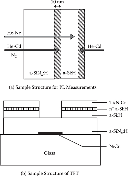
FIGURE 2.19 (a) A sample structure for photoluminescence measurements and a schematic illustration of the relationship between the observed region and the excitation light sources. (b) A sample structure of TFT.
2.5.2.3 Optical/Electrical Properties of a-SiNx:H Layers
Figure 2.20 shows various optical parameters of a-SiNx:H used in the present experiments as a function of nitrogen content x. The optical gap increases dramatically with increases in x when x > 0.85. The peak energy of the photoluminescence band (Epeak) also exhibits a high-energy shift. The values of B decrease when x increases from 0 to 0.85, and then, increase with x when x > 0.85. It is known that the structure of a-SiNx:H changes from tetrahedral to a Si3N4-like structure with increasing x.(20) Considering this, the results in Figure 2.20 suggest that the principal structural change occurs near the composition x = 0.85.
Resistivity of a-SiNx:H is in the order of 1015 Ωcm for x ≥ 0.93. For x = 0.85, although the resistivity decreases to 1013 Ωcm, the electron blocking property, necessary for TFT operation, is not lost.
2.5.2.4 Photoluminescence Spectra
Figure 2.21 shows the cw photoluminescence spectra of a-Si:H in an a-SiNx:H/aSi:H layered structure. Each curve corresponds to the result for the observed region in the a-Si:H. The spectra change from region to region. The photoluminescence band of a-Si:H near the interface appears in the low-energy side compared to that of the whole a-Si:H layer. The photoluminescence band of a-Si:H near the surface also exhibits a low-energy shift. These results suggest that the film property varies depending on the region of the a-Si:H layer. So, as described below, we can characterize the near-interface region of a-Si:H by the photoluminescence excited with a He-Cd laser.
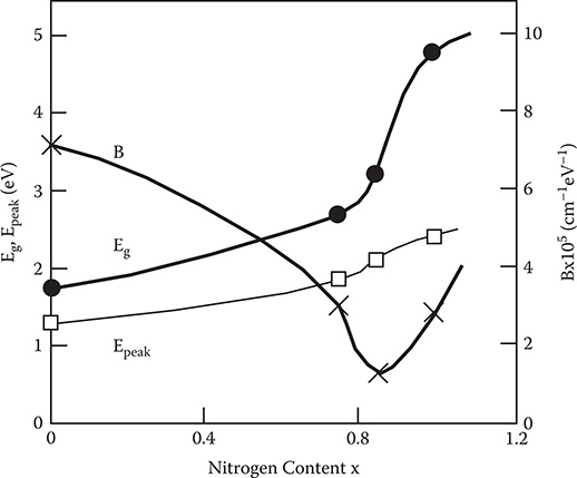
FIGURE 2.20 Optical parameters of a-SiNx:H used in the experiments. From T. Yoshimura, K. Hiranaka, T. Yamaguchi, and S. Yanagisawa, “Influence of a-SiNx:H composition on transfer-doping and electron trapping effects in a-SiNx:H/a-Si:H superlattices,” Philos. Mag. B 55, 409–416 (1987).
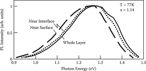
FIGURE 2.21 Cw photoluminescence spectra of a-Si:H in an a-SiNx:H/a-Si:H layered structure. From T. Yoshimura, K. Hiranaka, T. Yamaguchi, S. Yanagisawa, and K. Asama, “Characterization of a-SiNx:H/a-Si:H Interface by Photoluminescence Spectra,” Mat. Res. Soc. Symp. Proc. 70, 373–378 (1986).
Figure 2.22 shows the cw photoluminescence spectra of a-Si:H near the a-SiNx:H/ a-Si:H interface for various a-SiNx :H composition. Since the photoluminescence band is extremely broad, the peak position, EPL, is defined as follows.
where, EPL (−1/2) and EPL (+1/2) are the energy at the half maxima of the photoluminescence bands for the low-energy side and the high-energy side, respectively. As Figure 2.23 shows, EPL shifts to the low-energy side as the nitrogen content x of the a-SiNx:H layer increases.
To investigate the origin of the spectral shift observed in Figure 2.23, time-resolved photoluminescence spectra were measured with a pulsed nitrogen laser. Figure 2.24 shows the result for a sample with nitrogen content x = 1.24, which exhibits the largest low-energy shift of the photoluminescence band. After pulsed excitation, two broad bands are observed. The band on the high-energy side is denoted by the H-band and that on the low-energy side by the L-band. The H-band decays more rapidly than the L-band. The results shown in Figure 2.24 indicate that the cw photoluminescence band in Figure 2.22 contains two different broad bands. In Figure 2.25 the photoluminescence spectra of 2 µs after excitation are compared for x = 1.24, which shows the largest low-energy shift of the cw photoluminescence bands, and for x = 0.93, which shows the smallest low-energy shift in Figure 2.22. In x = 1.24, the L-band is more dominant than when x = 0.93. From this it is found that the 1ow-energy shift of the cw photoluminescence bands shown in Figure 2.23 can be attributed to an enhancement of the L-band.
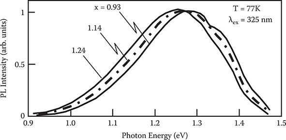
FIGURE 2.22 Cw photoluminescence spectra of a-Si:H near the a-SiNx:H/a-Si:H interface for x = 0.93, 1.14, and 1.24. From T. Yoshimura, K. Hiranaka, T. Yamaguchi, S. Yanagisawa, and K. Asama, “Characterization of a-SiNx:H/a-Si:H interface by photoluminescence spectra,” Mat. Res. Soc. Symp. Proc. 70, 373–378 (1986).
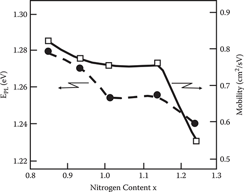
FIGURE 2.23 Dependence of EPL and field effect mobility in a-Si TFT on the nitrogen content of a-SiNx:H layer. From T. Yoshimura, K. Hiranaka, T. Yamaguchi, S. Yanagisawa, and K. Asama, “Characterization of a-SiNx:H/a-Si:H interface by photoluminescence spectra,” Mat. Res. Soc. Symp. Proc. 70, 373–378 (1986).
As illustrated in Figure 2.24, the H-band with a peak near 1.35 eV can be ascribed to transitions from band tail states since the photoluminescence peak arising from the inter-tai1 transition has been known to range between 1.3 and 1.4 eV at the delay of 0.5 − 5 µs [20]. The L-band is supposed to relate to some deep states. These results suggest that the low-energy shift of the cw photoluminescence band shown in Figure 2.23 is caused by an increase in the deep states in the a-Si:H layer. Namely, the more the band shifts to the low-energy side, the more deep states are induced. Therefore, it is concluded that the deep states in the a-Si:H layer increase with the nitrogen content x of the underlying a-SiNx:H layer.
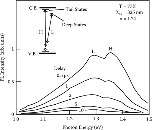
FIGURE 2.24 Time-resolved photoluminescence spectra of a-Si:H near the a-SiNx:H/a-Si:H interface. The insert is a schematic model of the deep states in the a-Si:H. From T. Yoshimura, K. Hiranaka, T. Yamaguchi, S. Yanagisawa, and K. Asama, “Characterization of a-SiNx:H/aSi:H interface by photoluminescence spectra,” Mat. Res. Soc. Symp. Proc. 70, 373–378 (1986).
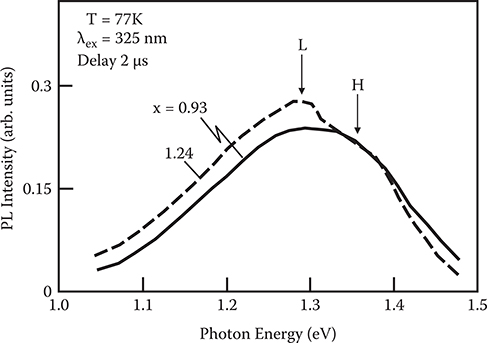
FIGURE 2.25 Photoluminescence spectra of a-Si:H near the a-SiNx:H/a-Si:H interface at 2 µs after pulsed excitation for x = 0.93 and 1.24. From T. Yoshimura, K. Hiranaka, T. Yamaguchi, S. Yanagisawa, and K. Asama, “Characterization of a-SiNx:H/a-Si:H interface by photoluminescence spectra,” Mat. Res. Soc. Symp. Proc. 70, 373–378 (1986).
In Figure 2.26, typical ID − VG characteristics are shown for an a-Si TFT with a gate insulator a-SiNx:H of x = 1.01. From Figure 2.23, it can be seen that the field effect mobility tends to decrease as the nitrogen content of the a-SiNx:H gate insulator increases, and the decrease in the field effect mobility correlates well with the low-energy shift of EPL. This correlation can be explained as follows. The field effect mobility in the TFT is reduced by the deep states in the a-Si:H layer near the interface corresponding to the low-energy shift of the photoluminescence band.
For the origin of the deep states, lattice strain induced in the a-Si:H layer may be considered as be1ow. Roxlo et al. identified lattice strain due to lattice mismatch [22]. Since it is known that the nearest neighbor interatomic distance of a-SiNx:H decreases from 0.24 to 0.17 nm as the nitrogen content increases from 0 to 4/3 [23], the difference in the nearest interatomic distance between a-SiNx:H and a-Si:H becomes large as x increases. This would cause large lattice strain and result in an increase in the deep states. This interpretation is consistent with the experimental results shown in Figure 2.23. In addition, as shown in Figure 2.20, the B value drastically increases with x for x > 0.9, suggesting that the lattice structure of a-SiNx:H is ordered to a Si3N4-1ike structure as x is increased. This would enhance the lattice mismatch between the a-SiNx:H layer and the tetrahedral a-Si:H 1ayer. The lattice strain would also be induced by stress effect. It was found that the stress of the a-SiNx:H layer monotonically changes from compressive to strong tensile stress as x increases from 0 to 1.24. This indicates that with increasing x, the stress difference between the a-SiNx:H layer and the a-Si:H layer becomes large. This would also result in an increase in the deep states due to the lattice strain.
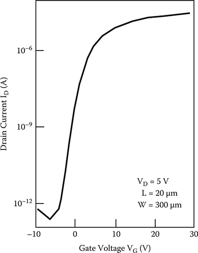
FIGURE 2.26 ID − VG characteristics of a-Si TFT. From T. Yoshimura, K. Hiranaka, T. Yamaguchi, S. Yanagisawa, and K. Asama, “Characterization of a-SiNx:H/a-Si:H interface by photoluminescence spectra,” Mat. Res. Soc. Symp. Proc. 70, 373–378 (1986).
It should be noted that with decreasing x, although mobility of a-Si TFTs increases, energy gaps of a-SiNx:H decrease as shown in Figure 2.27, which causes threshold voltage shifts of the TFTs due to electron injection from a-Si:H 1ayer into the a-SiNx:H layer. So, an energy gap of a-SiNx:H should be sufficiently larger than that of a-Si:H in TFTs.
2.5.3 TRANSFER-DOPING AND ELECTRON-TRAPPING EFFECTS IN A-SINx:H/A-SI:H SUPERLATTICES
2.5.3.1 Fabrication and Measurement Procedures
The a-SiNx:H/a-Si:H superlattice [18], whose structure is schematically illustrated in Figure 2.28, was formed by changing the composition of the reactive gases periodically in plasma CVD on glass or quartz substrates held at 230°C. All the samples have 12 a-Si:H layers and 13 a-SiHx:H layers. For the a-Si: H layers, 20% SiH4 diluted with H2 was used, and the flow rate, r.f. power, and pressure were 50 s.c.c.m., 1.5 W, and 20 Pa, respectively. The deposition rate was 3 nm/min. In the present experiments, the a-Si:H layer thickness, LS, was fixed to 10 nm. For the deposition of the a-SiNx:H layers, pure NH3 was added. The flow rate of 20% SiH4 diluted with H2 was kept constant at 50 sccm. To obtain a-SiNx:H with various compositions, the flow rate of the pure NH3 was varied from 25 to 150 sccm. The a-SiNx:H composition was estimated by Auger electron spectroscopy to be x = 0.75, 0.85, 1.0, and 1.15 for NH3 flow rates of 25, 50, 100, and 150 sccm, respectively. The plasma was interrupted for 1.5 min while the gases were changed.
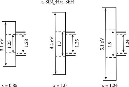
FIGURE 2.27 Band models of a-SiNx:H/a-Si:H layered structures.
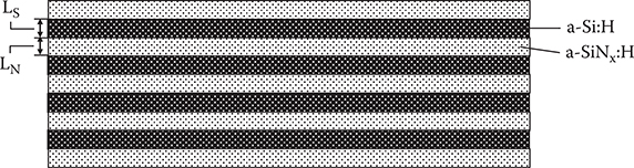
FIGURE 2.28 A structure of a-SiNx:H/a-Si:H superlattice.
We measured the in-plane conductivity by using slit-type electrodes with a 1-mm gap under 100-V bias. To form the electrodes, the superlattice film was scratched with a diamond scribe forming grooves 1 mm apart and Ag-paste colloidal solution was poured into the grooves and dried. This procedure should result in contact being made to all the layers. The samples were illuminated by a yellow LED (583 nm, 1 W/ m2) to measure the photocurrent. Before the dark current was measured, the samples were kept in the dark for 20 min. The activation energy of the dark current was obtained from Arrhenius plots in the temperature range of 30 to 100oC.
2.5.3.2 Transfer Doping
Figure 2.29(a) shows the influence of the nitrogen content x of a-SiNx:H on the dark conductivity, photoconductivity, and the activation energy of the dark current, EA, in the superlattices. It can be seen that in the range 0 < x < 0.85, the dark conductivity increases by three orders of magnitude with increasing x and reaches its maximum of 5 × 10⁻⁶ Ω−1cm−1 at x = 0.85. For x > 0.85, the dark conductivity decreases rapidly with increasing x. The photoconductivity exhibits a similar behavior. The activation energy of the dark conductivity has a minimum of 0.67 eV at x = 0.85, corresponding to the peak position of the dark conductivity and the photoconductivity. These results show that the transfer-doping effect is most effective at the nitrogen content x = 0.85.
The photocurrent enhancement in the amorphous superlattices is favorable from a viewpoint of applications to photovoltaic devices described in Chapter 9. Since in the superlattice large currents are generated in in-plane directions, planar-type photovoltaic devices with Schottky barriers might be available.
Figure 2.29(b) shows the influence of the a-SiNx:H thickness, LN, on the dark conductivity, photoconductivity, and the activation energy of the dark current for x = 0.85. The dark conductivity increases with increasing a-SiNx:H thickness and, at the same time, the activation energy decreases. This clearly indicates that, as shown in Figure 2.30, the transfer doping is mainly caused by electron transfer from the inner part of the a-SiNx:H layers to the a-Si:H layers rather than just from the interface states.
The reason why the transfer-doping effect becomes large at x = 0.85 can be considered from the optical properties of a-SiNx:H shown in Figure 2.20. In the range 0 < x < 0.85 it is supposed that a-SiNx:H has a tetrahedral structure and hence the concentration of donor-like states, arising from nitrogen atoms, increases with increasing x. For x > 0.85, on the other hand, the structure of a-SiNx:H tends toward that of Si3N4 in which nitrogen does not act as a donor. This leads to a decrease in the transfer-doping effect.
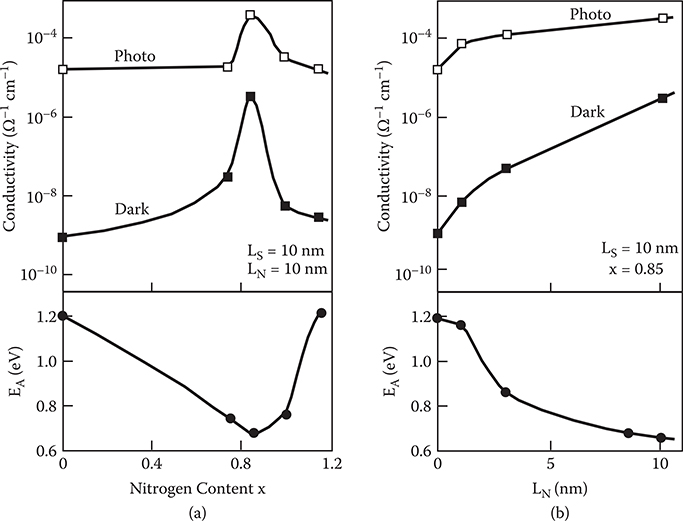
FIGURE 2.29 The dark conductivity, photoconductivity, and the activation energy of the dark current in the superlattices as a function of (a) the nitrogen content of a-SiNx:H and (b) the a-SiNx:H thickness. From T. Yoshimura, K. Hiranaka, T. Yamaguchi, and S. Yanagisawa, “Influence of a-SiNx:H composition on transfer-doping and electron trapping effects in a-SiNx:H/a-Si:H superlattices,” Philos. Mag. B 55, 409–416 (1987).
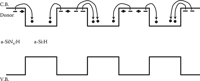
FIGURE 2.30 Schematic model for the transfer doping in a-SiNx:H/a-Si:H superlattices.
2.5.3.3 Electron Trapping
Figures 2.31(a) and (b) show decay curves of the photocurrent for various a-SiNx:H thicknesses, and thickness dependence of the half-decay time, τ1/2. The horizontal axis of (a) corresponds to time after the illumination is interrupted. As the a-SiNx:H layer thickness increases from 1 to 10 nm, the photocurrent decay becomes slow. This indicates that electron trapping by the a-SiNx:H layers occurs in the superlattice and extends to the inner part of the a-SiNx:H layers. The tendency for τ1/2 to saturate around LN ~ 10 nm indicates that the interaction depth for the electron-trapping phenomena is ~10 nm in the a-SiNx:H layer.
Figure 2.32 shows the photocurrent decay in the superlattice with LS = LN = 10 nm for various x at various measurement temperatures. A fast initial decay is observed in all the samples, followed by a slow decay component. The decay speed of the slow component depends on the a-SiNx:H composition. The slow component is greatly affected by temperature, while the fast component exhibits little temperature dependence. This indicates that the slow component is attributed to deep electron-trapping states in the a-SiNx:H layers and the process of the electron release from the deep states limits the decay time. Figure 2.33 shows the temperature dependence of the photocurrent decay time τ of the slow component for various x. Here, τ is the time for the slow component to decay to l/e of the initial value. For x = 0.75, τ increases with increasing T, whereas for x = 1.0, τ decreases with increasing T. For x = 0.85, τ increases with T if 1000/T < 3.2, and then decreases when 1000/T > 3.2. Thus electron trapping by the a-SiNx:H layers varies strongly with the a-SiNx:H composition.
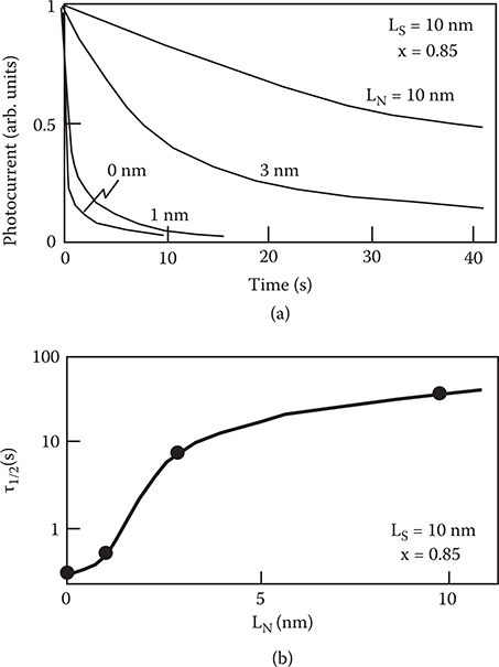
FIGURE 2.31 (a) Photocurrent decay curves for various a-SiNx:H thicknesses, and (b) thickness dependence of the half-decay time of the photocurrent decay curves, in a-SiNx:H/a-Si:H superlattices. From T. Yoshimura, K. Hiranaka, T. Yamaguchi, and S. Yanagisawa, “Influence of a-SiNx:H composition on transfer-doping and electron trapping effects in a-SiNx:H/a-Si:H superlattices,” Philos. Mag. B 55, 409–416 (1987).
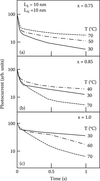
FIGURE 2.32 Photocurrent decay in a-SiNx:H/a-Si:H superlattices at various measurement temperatures for (a) x = 0.75, (b) x = 0.85, and (c) x = 1.0. From T. Yoshimura, K. Hiranaka, T. Yamaguchi, and S. Yanagisawa, “Influence of a-SiNx:H composition on transfer-doping and electron trapping effects in a-SiNx:H/a-Si:H superlattices,” Philos. Mag. B 55, 409–416 (1987).
As reported by Rose [24], τ versus T characteristics are determined by the relationship between the position of the Fermi level and the distribution of the electron-trapping states. When the Fermi level is located in the middle of a continuous distribution of electron-trapping states, τ increases with T. Conversely, when the states are located above the Fermi level, τ decreases with T. According to this, qualitative models for the electron-trapping states are schematically illustrated as in Figure 2.34. For x = 0.75, the Fermi level is in the middle of the electron-trapping states. For x = 1.0, the Fermi level is below the electron-trapping states. For x = 0.85, the Fermi level should be near the bottom of the electron-trapping states, since τ decreases with T in the range of 1000/T > 3.2.
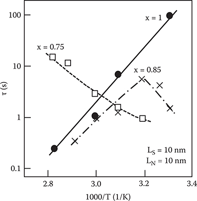
FIGURE 2.33 Temperature dependence of the photocurrent decay time of the slow component. From T. Yoshimura, K. Hiranaka, T. Yamaguchi, and S. Yanagisawa, “Influence of a-SiNx:H composition on transfer-doping and electron trapping effects in a-SiNx:H/a-Si:H superlattices,” Philos. Mag. B 55, 409–416 (1987).
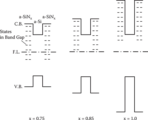
FIGURE 2.34 Schematic model for the electron-trapping-state distribution in the a-SiNx:H layer. From T. Yoshimura, K. Hiranaka, T. Yamaguchi, and S. Yanagisawa, “Influence of a-SiNx:H composition on transfer-doping and electron trapping effects in a-SiNx:H/a-Si:H superlattices,” Philos. Mag. B 55, 409–416 (1987).
2.6 Sputtering
Sputtering is one of the popular thin-film deposition methods. It enables us to control crystallinity and composition, that is, atomic arrangements in thin films, by adjusting sputtering power, gas composition and pressure, substrate temperature, and source material composition. This section describes an example of material property control by film structures in an atomic level, and enhancement of coloration efficiency in WOx electrochromic thin films by sputtering [25, 26].
2.6.1 ELECTROCHROMISM IN WOx THIN FILMS
WOx thin films exhibit electrochromism [27]. The coloration is attributed to color centers generated by electrons injected in the films. Since the absorption spectra of the color centers cover the visible and near infrared regions, WOx thin films are useful for displays and heat-cut windows.
Figure 2.35 shows the coloring/bleaching mechanism in electrochromic devices (ECDs). ECD consists of an electrochromic layer of WO3 and electrolyte that are sandwiched by an indium tin oxide (ITO) electrode and a counter electrode. By applying negative voltage to the ITO electrode, electrons are injected into the WO3 thin film, and at the same time, protons are injected to the film from the electrolyte to cancel the negative charge of the injected electrons. Due to the neutralization, many electrons can be injected into the WO3 thin film, say, several tenths of the number of W atoms in the film. The injected electrons are trapped at W6+ sites to form color centers. The trapped electrons hop to the neighboring W6+ sites by absorbing light. The light absorption contributes to the coloration of WO3. By making the external circuits open, the injected charge is kept in the film, giving rise to memory function as well as battery function. By shorting the ITO and counter electrodes, the electrons and protons are ejected from the WO3 thin film to bleach the film.
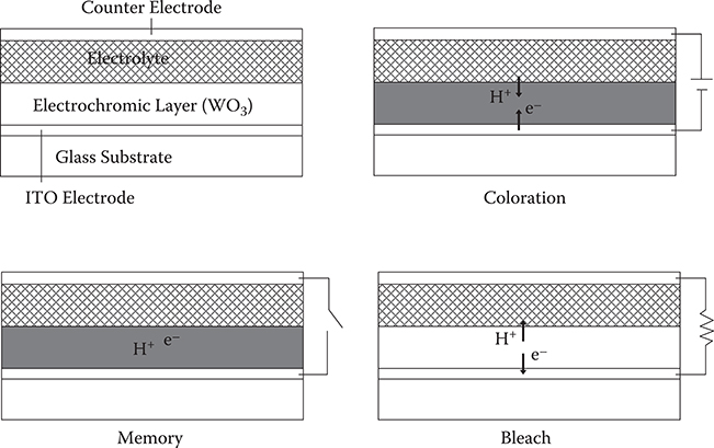
FIGURE 2.35 Coloring/bleaching mechanism in electrochromic devices (ECDs).
Since WO3 is an n-type semiconductor, it is expected to be applied to photovoltaic devices having battery function, which is described in Chapter 9, Section 9.4.
2.6.2 ENHANCEMENT OF COLORATION EFFICIENCY IN WOx WITH CONTROLLED FILM STRUCTURES
The coloration property of WO3 is affected by the film structures, that is, atomic arrangements in the film. We fabricated two kinds of ECDs with a WO3 thin film deposited from WO3 powder and a “WO2” thin film from WO2 powder using vacuum evaporation [26]. Figure 2.36 shows the absorption spectra of the color canters in WO3 and “WO2” thin films for the same injected charge (~3 mC/cm2). The “WO2” thin film has much larger absorption than does the WO3 thin film.
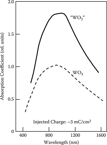
FIGURE 2.36 Absorption spectra of the color centers in WO3 and “WO2” thin films for the same injected charge. From T. Yoshimura, M. Watanabe, Y. Koike, K. Kiyota, and M. Tanaka, “Enhancement in oscillator strength of color centers in electrochromic thin films deposited from WO2,” J. Appl. Phys. 53, 7314–7320 (1982).
In order to reveal the reason for the difference in the absorption property, precise investigation was carried out using rf reactive magnetron sputtering [25]. Figure 2.37 shows the coloration efficiency spectra of WOx thin films deposited at an oxygen gas pressure of 3 Pa at various rf powers. The efficiency is drastically enhanced as rf power increases. At rf power of 1000 W, the peak height is seven times greater than that of the conventional WOx thin film prepared by vacuum evaporation. In Figure 2.37, it is noted that, with an increase in the efficiency, the peak position of the efficiency spectra shifts to the low-energy side.
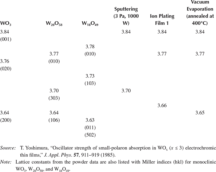
Table 2.3 lists the lattice constants obtained by x-ray diffraction measurements on the film prepared by rf reactive magnetron sputtering, reactive ion plating, and vacuum evaporation. In the left-hand columns of the table, the powder data for monoclinic WO3, W20O58, and W18O49 are shown for reference.
Figure 2.38 shows typical x-ray photoelectron spectroscopy (XPS) spectra of W4f and O1s levels in WOx thin films deposited by rf reactive magnetron sputtering. The intensity of the XPS spectrum for O1s level decreases with an increase in rf power, while that for the W4f level shows a slight difference among the three films. Table 2.4 lists the counting ratio of photoelectrons from the O1s level to those from the W4f level for the WOx thin films. The counting ratio was calculated by integrating the line profiles of the XPS spectra.
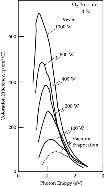
FIGURE 2.37 Coloration efficiency spectra of WOx thin films deposited by rf reactive magnetron sputtering for various rf powers. From T. Yoshimura, “Oscillator strength of small-polaron absorption in WOx (x≤3) electrochromic thin films,” J. Appl. Phys. 57, 911–919 (1985).
TABLE 2.3
Lattice Constants Obtained from X-Ray Diffraction Patterns for Various WOx Thin Films
Although the counting ratio of O1s/W4f itself does not give the O/W ratio in the film directly, we can obtain qualitative information about the O/W ratio by comparing the counting ratio of O1s/W4f for the various WOx thin films. It can be seen from Table 2.4 that oxygen content in the film decreases with increasing rf power, which is consistent with the change in film structure induced by increasing rf power, that is, development of a W20O58 structure in WOx thin film. Comparing the results shown in Figure 2.37 with the counting ratio of O1s/W4f and the x-ray diffraction patterns described above, we can find the clear correlation between the enhancement of coloration efficiency and a lack of oxygen in the WOx thin film, which induces the W20O58-like structure.
In Figure 2.39, a model for the light absorption in WO3, called small-polaron absorption [27], is schematically illustrated as well as the lattice structure of WO3. The crystal structure of WO3 is a corner-shared WO6 octahedral. Each W site is surrounded by six O sites. When an injected electron is trapped at the WA site, the electron distorts the surrounding lattice, forming a small polaron. When the electron is transferred to the neighboring WB site by absorbing light, the distortion is also transferred to the WB site. This means that the small polaron hops from the WA site to the WB site. So, the light absorption caused by the trapped electron in WO3 is called small-polaron absorption.
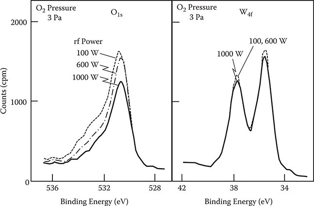
FIGURE 2.38 Typical XPS spectra of the W4f and O1s levels in WOx thin films deposited by rf reactive magnetron sputtering. From T. Yoshimura, “Oscillator strength of small-polaron absorption in WOx (x≤3) electrochromic thin films,” J. Appl. Phys. 57, 911–919 (1985).
TABLE 2.4
Counting Ratio of Photoelectrons from O1s Level to Those from the W4f Level for WOx Thin Films
| Oxygen Pressure (Pa) |
|
3 |
|
| rf Power (W) | 100 |
600 |
1000 |
| O1s/W4f Ratio | 0.95 |
0.8 |
0.7 |
Source: T. Yoshimura, “Oscillator strength of small-polaron absorption in WOx (x ≤ 3) electrochromic thin films,” J. Appl. Phys. 57, 911–919 (1985).
Faughnan et al. determined that the oscillator strength of the absorption band in the evaporated WOx thin film is f0 = 0.1 [28]. Then, oscillator strength of the small-polaron absorption is estimated for various WOx thin films using the following expression:
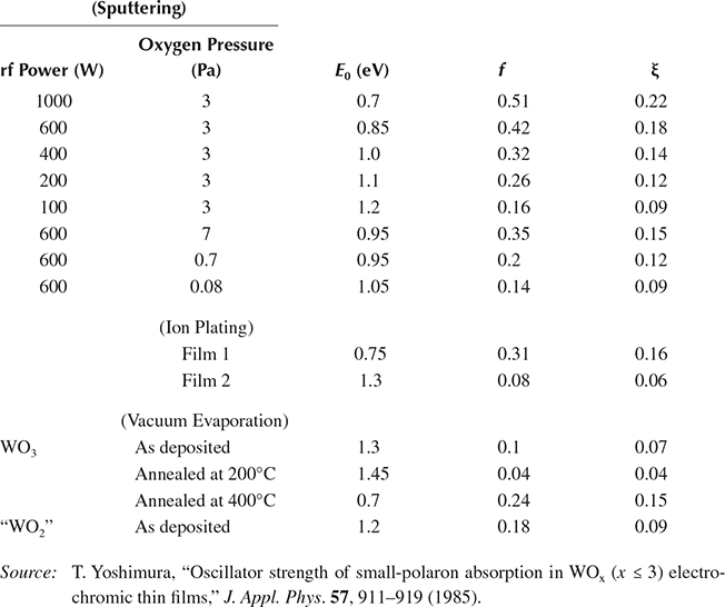
Here, I and Io are respectively the integrated intensity of the coloration efficiency spectra of WOx thin films and that of a WOx thin film prepared by vacuum evaporation. Table 2.5 lists the oscillator strength f and the peak position E0 of absorption band for various WOx thin films. Oscillator strength varies widely depending on the procedure used for the film preparation. An extremely large oscillator strength is obtained for the film deposited by rf reactive magnetron sputtering at 1000 W. The value is five times larger than that of a conventional evaporated WOx thin film, and one order of magnitude larger than that of the evaporated film annealed at 200oC in air.
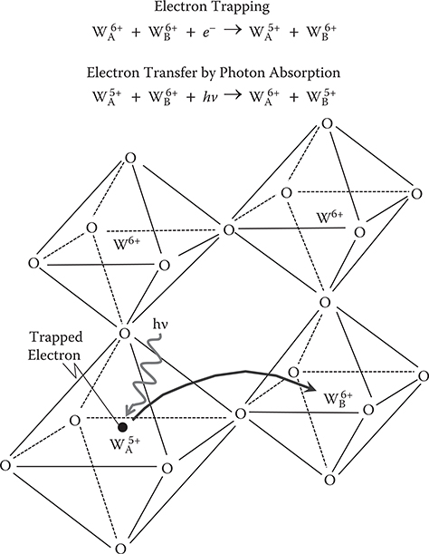
FIGURE 2.39 Schematic illustration of a lattice structure, and a model for the small-polaron absorption in WO3. From T. Yoshimura, “Oscillator strength of small-polaron absorption in WOx (x≤3) electrochromic thin films,” J. Appl. Phys. 57, 911–919 (1985).
The mechanism of the oscillator strength enhancement can be discussed from the viewpoint of the degree of polaron extension. Faugnan et al. reported that f, E0, in eV, and the dipole strength D in nm are related as follows [28].
Considering that each W5+ site is surrounded by six neighboring W6+ sites, D is given by
TABLE 2.5
Properties of Small-Polaron Absorption for Various WOx Thin Films
where r is nearest W–W distance in nm, and ξ is the delocalization parameter of the polaron wavefunction. ξ has the following physical meaning: when an electron is trapped at a W site, the wavefunction of the trapped electron is not completely localized at the site, but a fraction of the wavefunction ξ penetrates to the neighboring W site. Substituting Equation (2.2) into Equation (2.1), f is expressed in terms of E0 and ξ as follows:
In this equation, it must be noted that E0 is also a function of ξ as will be qualitatively explained by the configuration coordinate diagram in Figure 2.40. ξ can be determined by substituting E0, f, and r into Equation (2.3). The nearest W–W distance in the crystalline WO3, 0.54 nm, is used for r as a zeroth approximation. The obtained values of ξ are listed in Table 2.5.
It should be noted in Table 2.5 that f increases from 0.04 to 0.51 as ξ increases from 0.04 to 0.22. This relationship between f and ξ can be explained as follows. As can be seen from Figure 2.39, the oscillator strength of the absorption band is expected to increase with an increase in the transition probability for the electron to hop from the WA site to the WB site. If the trapped electron is completely localized, that is, ξ = 0, transition probability is reduced to zero since the initial state wavefunction (trapped state at the WA site) does not overlap with the final state (trapped state at the WB site). With an increase in penetration of wavefunction to the neighboring WB site, that is, an increase in ξ, the overlap of the wavefunction between the initial and the final states increases, causing the transition probability to become larger.
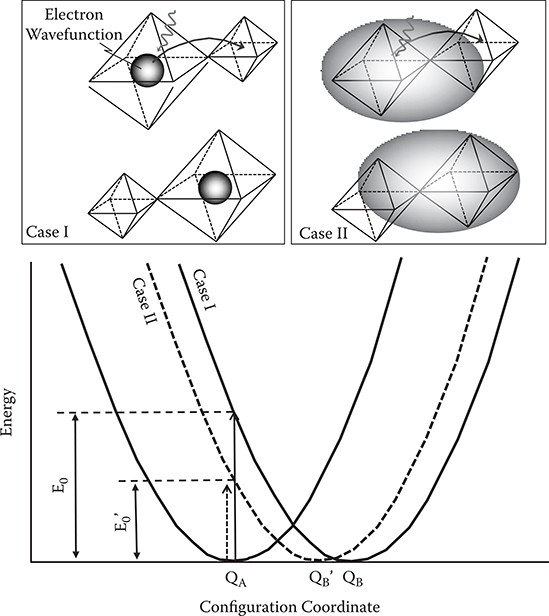
FIGURE 2.40 Configuration coordinate diagrams for small-polaron absorption. From T. Yoshimura, “Oscillator strength of small-polaron absorption in WOx (x ≤ 3) electrochromic thin films,” J. Appl. Phys. 57, 911–919 (1985).
The previously descrbed behavior of the oscillator strength is explained by a configuration coordinate diagram for small-polaron absorption, proposed by Faughnan et al., [28]. In Figure 2.40, QA or QB is the equilibrium position of the lattice surrounding the electron, which is trapped at the WA site or the WB site, respectively. When an electron trapped at the WA site is excited by absorbing a photon with energy E0, it transfers from the initial state to the final state (trapped at the WB site). After the transition of the electron, a relaxation of the surrounding lattice occurs along the curve with a minimum point at QB. So, ΔQ = QB – QA represents the change of lattice distortion, accompanied by the electron hopping from the WA site to the WB site.
Since ΔQ = QB – QA corresponds to the change of lattice distortion induced by the electron hopping, ΔQ depends on the degree of localization of the trapped electron. When the trapped electron is highly localized (Case I in Figure 2.40), the lattice distortion is large because, at first, lattice distortion is well localized around the WA site, then, it shifts around the WB site following the transfer of the electron from WA to WB. With delocalization of the trapped electron (Case II in Figure 2.40), the lattice distortion becomes small, indicating that ΔQ decreases. Since ξ represents the penetrating fraction of the trapped electron into the neighboring site, the degree of delocalization of the trapped electron increases with an increase in ξ . Therefore, it is suggested that ΔQ will decrease with an increase in ξ, implying that the energy curve for the WB site in the configuration coordinate diagram shifts from the solid curve to the dotted curve with increasing ξ. In this case, then, it is expected that the peak position of the absorption band shifts to the low-energy side with an increase in ξ.
Figure 2.41 shows the relationship between experimentally obtained E0 and ξ. It is found that E0 tends to decrease with increasing ξ as expected from the previously mentioned configuration coordinate model. Thus, it is confirmed that the enhancement of the oscillator strength of small-polaron absorption arises from a development of delocalization of the polaron wavefunction.
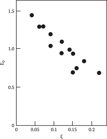
FIGURE 2.41 Relationship between experimentally obtained E0 and ξ. From T. Yoshimura, “Oscillator strength of small-polaron absorption in WOx (x ≤ 3) electrochromic thin films,” J. Appl. Phys. 57, 911–919 (1985).
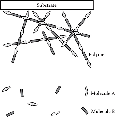
FIGURE 2.42 Mechanism of the vacuum deposition polymerization.
As described, by controlling sputtering conditions, the atomic arrangements in the films are controlled, which enables control of optical properties of the film, such as oscillator strength, namely, coloration efficiency.
2.7 Vacuum Deposition Polymerization
Vacuum deposition polymerization, shown in Figure 2.42, is a method for polymer film deposition in vacuum using vacuum evaporation [29, 30, 31 and 32]. Two kinds of reactive molecules A and B are evaporated in a vacuum chamber. The molecules are combined to deposit polymer films on the substrate surface. Vacuum deposition polymerization is regarded as CVD for polymer film fabrication.
Various applications of vacuum deposition polymerization have been reported, such as polyimide films for nonlinear optical materials, organic EL devices, insulators in multilayer circuit substrates and LSIs, surface coating, and so on.
Weaver and Bradley demonstrated that the chemical vapor deposition polymerization is an effective method to fabricate conjugated polymer films of polyazomethine (poly-AM) in the organic EL [33]. The result confirms that vacuum deposition polymerization is useful to grow functional polymer films, and at the same time, confirms the prospect of applications of poly-AM to thin-film organic photonic/electronic devices.
References
1. E. Buks, R. Schuster, M. Heiblum, D. Mahalu, and V. Umansky, “Dephasing in electron interference by a ‘which-path’ detector,” Nature 391, 871–874 (1998).
2. D. M. Eigler and E. K. Schweizer, “Positioning single atoms with a scanning tunneling microscope,” Nature 344, 524–526 (1990).
3. M. F. Crommie, C. P. Lutz, and D. M. Eigler, “Confinement of electrons to quantum corrals on a metal surface,” Science 262, 218–220 (1993).
4. H. C. Manoharan, C. P. Lutz, and D. M. Eigler, “Quantum mirages formed by coherent projection of electronic structures,” Nature 403, 512–515 (2000).
5. L. Esaki and R. Tsu, “Superlattice and negative differential conductivity in semiconductors,” IBM Journal of Research and Development 14, 61–65 (1970).
6. T. Mimura, S. Hiyamizu, T. Fujii, and K. Nanbu, “A new field-effect transistor with selectively doped GaAs/n-AlxGa1-xAs heterojunctions,” Jpn. J. Appl. Phys. 19, L225–L227 (1980).
7. D. S. Chemla, D. A. B. Miller, and P. W. Smith, “Nonlinear optical properties of GaAs/GaAlAs multiple quantum well material: Phenomena and applications,” Opt. Eng. 24, 556–564 (1985).
8. T. Suntola, “Atomic layer epitaxy,” Material Science Reports 4 (7), 1989, Elsevier Science Publishers.
9. F. Roozeboom, W. Dekker, K. B. Jinesh, J. H. Klootwijk, M. A. Verheijen, H.D. Kim, and D. Blin, “Ultrahigh-density trench decoupling capacitors comprising multiple MIM layer stacks grown by atomic layer deposition,” AVS, 8th International Conference on Atomic Layer Deposition, MonA1-1, Bruges, Belgium (2008).
10. J. H. Shim, J. S. Park, J. An, T. M. Gur, and F. B. Prinz, “Atomic layer deposition of proton conducting Y:BaZrO3,” AVS, 9th International Conference on Atomic Layer Deposition, Monterey, California, 76 (2009).
11. H. Shin and C. Bae, “Nanoscale tubular structures and ampoules of oxides,” AVS, 8th International Conference on Atomic Layer Deposition, TueM2-1, Bruges, Belgium (2008).
12. G. N. Parsons, Q. Peng, J. C. Spagnola, G. Scarel, G. K. Hyde, B. Gong, C. Devine, K. Lee, J. Jur, K. Roberts, and J. S. Na, “Modification of fibers and nonwoven fiber mats using atomic layer deposition,” AVS, 9th International Conference on Atomic Layer Deposition, Monterey, California, 29 (2009).
13. D. H. Levy, D. C. Freeman, S. F. Nelson, and P. J. Cowdery-Corvan, “A high-speed continuous process for ALD depositions,” AVS, 8th International Conference on Atomic Layer Deposition, WedA2b-3, Bruges, Belgium (2008).
14. C. B. Roxlo, B. Abeles, and T. Tiedje, “Amorphous semiconductor superlattices,” Phys, Rev. Lett. 51, 2003–2006 (1983).
15. T. Tiedje and B. Abeles, “Charge transfer doping in amorphous semiconductor superlattice,” Appl. Phys. Lett. 45, 179–181 (1984).
16. J. Kakalios, H. Fritzsche, N. Ibaraki, and S. R. Ovshinsky, “Properties of amorphous semiconducting multilayer films” J. Non-Crystalline Solids 66, 339–344 (1984).
17. M. J. Powell, “Charge trapping instabilities in amorphous silicon-silicon nitride thin-film transistors,” Appl. Phys. Lett. 43, 597–599 (1983).
18. T. Yoshimura, K. Hiranaka, T. Yamaguchi, and S. Yanagisawa, “Influence of a-SiNx:H composition on transfer-doping and electron trapping effects in a-SiNx:H/a-Si:H super-lattices,” Philos. Mag. B 55, 409–416 (1987).
19. T. Yoshimura, K. Hiranaka, T. Yamaguchi, S. Yanagisawa, and K. Asama, “Characterization of a-SiNx:H/a-Si:H interface by photoluminescence spectra,” in Materials issues in amorphous-semiconductor technology, edited by D. Adler, Y. Hamakawa, and A. Madan (Mater. Res. Soc. Symp. Proc. 70, 373–378, (1986).
20. T. V. Herak, R. D. Meleod, K. C. Kao, H. C. Card, H. Watanabe, K. Katoh, M. Yasui, and Y. Shibata, “Undoped amorphous SiNx:H alloy semiconductors: Dependence of electronic properties on composition,” J. Non-Crystalline Solids 69, 39–48 (1984).
21. C. Tsang and R. A. Street, “Recombination in plasma-deposited amorphous Si:H luminescence decay,” Phys. Rev. B 19, 3027–3040 (1979).
22. C. B. Roxlo, B. Abeles, and T. Tiedje, “Evidence for lattice-mismatch-induced defects in amorphous semiconductor hetero-junctions,” Phys. Rev. Lett. 52, 1994–1997 (1984).
23. K. Tanaka, Fundamentals of amorphous semiconductors, (Ohmusha, Tokyo, 1982) [in Japanese].
24. A. Rose, “Outline of some photoconductive processes,” RCA Rev. 12, 362–414 (1951).
25. T. Yoshimura, “Oscillator strength of small-polaron absorption in WOx (x ≤ 3) electro-chromic thin films,” J. Appl. Phys. 57, 911–919 (1985).
26. T. Yoshimura, M. Watanabe, Y. Koike, K. Kiyota, and M. Tanaka, “Enhancement in oscillator strength of color centers in electrochromic thin films deposited from WO2,” J. Appl. Phys. 53, 7314–7320 (1982).
27. S. K. Deb, “Optical and photoelectric properties and colour centres in thin films of tungsten oxide,” Pholos. Mag. 27, 801–822 (1973).
28. B. W. Faughnan, R. S. Crandall, and D. Heyman, “Electrochromism in WO3 amorphous films,” RCA Rev. 36, 177–197 (1975).
29. M. Iijima, Y. Takahashi, K. Inagawa, and A. Itoh, J. Vac. Soc. Jpn. 28, 437 (1985) [in Japanese].
30. Y. Takahashi, M. Iijima, K. Iinagawa, and A. Itoh, “Synthesis of aromatic polyimide film by vacuum deposition polymerization,” J. Vac. Sci. Technol. A 5, 2253–2256 (1987).
31. M. Iijima, Y. Takahashi, and E. Fukuda, “Vacuum deposition polymerization,” Nikkei New Materials, December 11, 93–100 (1989) [in Japanese].
32. A. Kubono, N. Okui, K. Tanaka, S. Umemoto, and T. Sakai, “Highly oriented polyamide thin films prepared by vapor deposition polymerization,” Thin Solid Films 199, 385–393 (1991).
33. M. S. Weaver and D. D. C. Bradley, “Organic electroluminescence devices fabricated with chemical vapour deposited polyazomethine films,” Synthetic Metals 83, 61–66 (1996).