
8 Applications to Optical Interconnects and Optical Switching Systems
Chapters 1 through 7 covered artificial materials with atomic/molecular-level tailored structures including polymer wires and molecular wires, and fabrication processes for the artificial materials including molecular layer deposition (MLD). Related thin-film organic photonic/electronic materials and devices, as well as integration processes were also described.
In the present chapter, possible applications of these materials and processes to OE systems such as optical interconnects and optical switching systems are presented, and the impact of the polymer multiple quantum dots (MQDs) built by MLD are discussed.
8.1 3-D Optoelectronic (OE) Platform Based On Scalable Film Optical Link Module (S-FOLM)
The three-dimensional (3-D) optoelectronic (OE) platform is a concept involves thin-film photonic devices embedded in films that are connected by optical waveguides three-dimensionally to provide various kinds of functions including optical wiring, optical switching, and so on.
The 3-D OE platform is based on scalable film optical link modules (S-FOLM) [1, 2, 3, 4, 5 and 6]. Figure 8.1 shows the concept of S-FOLM. First, a set of thin-film-device-embedded OE films are prepared. The thin-film devices include optical waveguides, vertical cavity surface-emitting lasers (VCSELs), photodetectors (PDs), light modulators, optical switches, wavelength filters, photovoltaic devices, driver/amplifier integrated circuits (ICs), large-scale integrated circuits (LSIs), lenses, mirrors, and so on. By combining the OE films with stacked configurations, various kinds of OE systems are constructed.
By stacking a VCSEL/PD-embedded OE film on an LSI, an OE LSI will be available. When an OE film containing a VCSEL/PD/optical waveguide and an OE film containing IC are stacked, an optical interconnect board is created. If LSI-embedded OE films are added in the stack, a 3-D OE LSI is created. If optical-switch-embedded OE films are used in the stack, a three-dimensional micro-optical switching system (3D-MOSS) will be available [7,8]. When photovoltaic devices are embedded in OE films, solar energy conversion systems will be provided [9, 10, 11, 12 and 13]. Such scalability enables S-FOLM to be used for the 3-D OE platform, which contributes to system cost reduction.
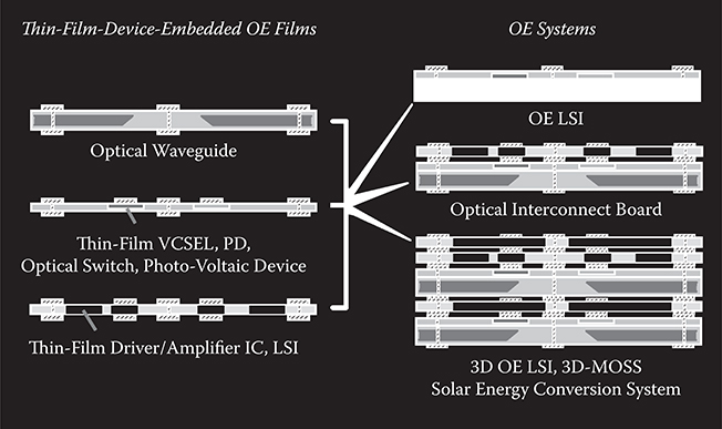
FIGURE 8.1 The S-FOLM concept. From T. Yoshimura, J. Roman, Y. Takahashi, M. Lee, B. Chou, S. Beilin, W. Wang, and M. Inao, “Optoelectronic scalable substrates based on film/Z-connection and its application to film optical link module (FOLM),” Proc. SPIE 3952, 202–213 (2000).
8.2 Optical Interconnects Within Boxes
Within boxes of computers, increases in clock frequency and wiring density cause problems such as RC delay, signal attenuation, power dissipation, and cross-talk. One of the solutions for these problems is the 3-D architecture, which can reduce wiring distances. Another solution is the optical interconnect, which can reduce RC delay, electromagnetic induction and interference, and frequency-dependent signal loss. Due to principled advantages of optical interconnects over electrical interconnects [14], it is expected that optics will be implemented within boxes [15, 16, 17, 18, 19, 20, 21 and 22].
Optics were first implemented into long-haul communication systems. It has recently been implemented in shorter-distance systems, such as local area network (LAN) and box-to-box data transmission. For within-box data transmission, the connection channel count is several hundreds to thousands. It is larger than that in conventional OE modules for box-to-box interconnects by one to two orders of magnitude. This means that electrical-to-optical (E-O) and optical-to-electrical (O-E) conversion devices of several hundreds to thousands should be distributed on a board. To achieve such high density, the size and cost of the conversion device should be reduced by one to two orders of magnitude.
We have proposed a low-cost solution for these problems using the 3-D OE platform, where the 3-D architectures and optical interconnects are implemented [1–6].
8.2.1 Multilayer OE Boards And 3-D Stacked OE Multi-Chip Modules
Figure 8.2 shows a multilayer OE board and a 3-D stacked OE multi-chip-module (MCM) based on the 3-D OE platform. In the multilayer OE board [1, 2, 3 and 4], a plurality of optical waveguide films with 45° reflectors are stacked. Thin-film active devices such as light modulators and PDs are embedded for E-O and O-E conversions. In the example shown in Figure 8.2, E-O and O-E conversions are performed in the second layer from the top, where thin-film active devices are embedded. The third and fourth layers are used for multilayer optical signal routing, which avoids wiring interference in high-density interconnect systems.
The first layer is an interface film, where thin-film ICs are embedded. On the interface film, LSIs are mounted. The thin-film ICs in the interface films may perform the functions of MUX/DMUX, error correction, and drivers/amplifiers, providing standardized interface capability.
When we use OE amplifier/driver-less substrate (OE-ADLES) (described in Section 8.2.2), where E-O and O-E conversions are respectively carried out by light modulators that are directly driven by LSI output and by PDs that directly generate LSI input, the interface film is not necessary. OE-ADLES is expected to have low power dissipation and high data rate capabilities [23, 24 and 25].
In 3-D stacked OE MCM [1–8], light modulator/PD-embedded waveguide films are stacked together with films containing thin-film LSIs. The structure can be regarded as 3-D stacked OE LSI when the stacked thin-film LSIs are divided chips corresponding to blocks of an LSI chip. This structure is the goal of the 3-D OE platform for computers because it realizes 3-D wiring and optical wiring simultaneously. In the 3-D stacked OE MCM, heat generation is a serious problem. So implementation of OE-ADLES that uses high power external light sources might be mandatory for power dissipation reduction within the 3-D OE platform. By setting light sources with a plurarity of wavelengths, wavelength division multiplexing (WDM) can be performed in the interconnect systems.
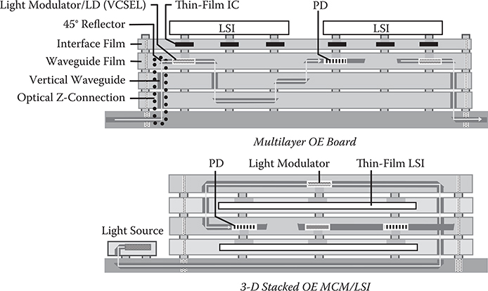
FIGURE 8.2 Schematic illustrations of a multilayer OE board and a 3-D stacked OE MCM/LSI. From T. Yoshimura, T. Inoguchi, T. Yamamoto, S. Moriya, Y. Teramoto, Y. Arai, T. Namiki, and K. Asama, “Self-organized lightwave network based on waveguide films for three-dimensional optical wiring within boxes,” J. Lightwave Technol. 22, 2091–2100 (2004).
Optical Z-connections in the 3-D OE platform are used to achieve optical links between the stacked waveguide films, constructing 3-D optical wiring. The optical Z-connections consist of two 45° reflectors built in the waveguide films. For long-distance connections, vertical waveguides are inserted between the 45° reflectors.
The optical interconnects based on the 3-D OE platform consisting of S-FOLM have the following advantages:
Excess module spaces for E-O and O-E conversions are not necessary, resulting in size reduction.
Long electrical lines for connection between LSI pads and E-O and O-E conversion sites are replaced with short vertical electrical lines, resulting in latency and bit error rate reduction.
Material consumption for the devices can be saved by PL-Pack with SORT, resulting in cost reduction.
Alignment between optical waveguides and thin-film devices can be performed by photolithography, resulting in low assembly cost.
Relative positions between optical waveguides and thin-film device flakes • are insensitive to temperature, resulting in thermal stability.
Flexible interface specification is possible by inserting interface films, permitting computer engineers to use conventional design tools without knowledge of optics.
Multilayer structures are easily constructed by film stacking.
Thus, it is concluded that the key issue for optical interconnects within boxes, that is, drastic size and cost reduction, can be accomplished by S-FOLM implementation.
The main core technologies for the multilayer OE board and the 3-D stacked OE MCM are summarized in Figure 8.3, including high-speed, small-sized light modulators and optical switches described in Chapter 6, OE films of optical waveguides with vertical reflectors and 3-D optical wiring as described in Section 7.6, SOLNET as described in Section 7.4, and resource-saving heterogeneous integration by PL-Pack with SORT as described in Section 7.5. The polymer MQD fabricated by MLD contributes to improving the performance of the light modulators and optical switches.
8.2.2 OE Amplifier/Driver-Less Substrate (OE-ADLES)
To reduce power dissipation and increase the data rate, we proposed OE-ADLES [23–25]. Figure 8.4 shows OE-ADLES for the OE MCM. E-O and O-E conversions are respectively carried out by light modulators and PDs, which are completely embedded in OE films. LSI I/O pads are connected to electrodes of the light modulators and PDs. Strong light beams are introduced from outside into the OE MCM via an OE printed circuit board (PCB). The external light beams are directly modulated by LSI output through the light modulators without drivers. The generated optical signals are transmitted through optical waveguides to the PDs, where the optical signals are converted back to electrical signals for LSI input without amplifiers. OE-ADLES is expected to have low power dissipation and high data rate capabilities for the following reasons:
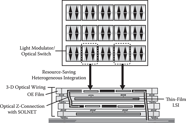
FIGURE 8.3 Main core technologies for the multilayer OE board and the 3-D stacked OE MCM.
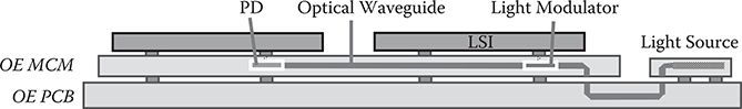
FIGURE 8.4 OE-ADLES for OE MCM. From T. Yoshimura, Y. Suzuki, N. Shimoda, T. Kofudo, K. Okada, Y. Arai, and K. Asama, “Three-dimensional chip-scale optical interconnects and switches with self-organized wiring based on device-embedded waveguide films and molecular nanotechnologies,” Proc. SPIE 6126, 612609-1-15 (2006).
Light sources are placed outside, reducing power dissipation within the interconnect systems.
Light modulators, which are voltage-driven devices, are used for transmitters, reducing driving power and rising/falling time for optical signal generation.
Strong light is available from external sources (high-power LD, mode-locked LD), achieving fast response of PDs.
8.2.3 IMPACT OF POLYMER MQDS ON OE-ADLES
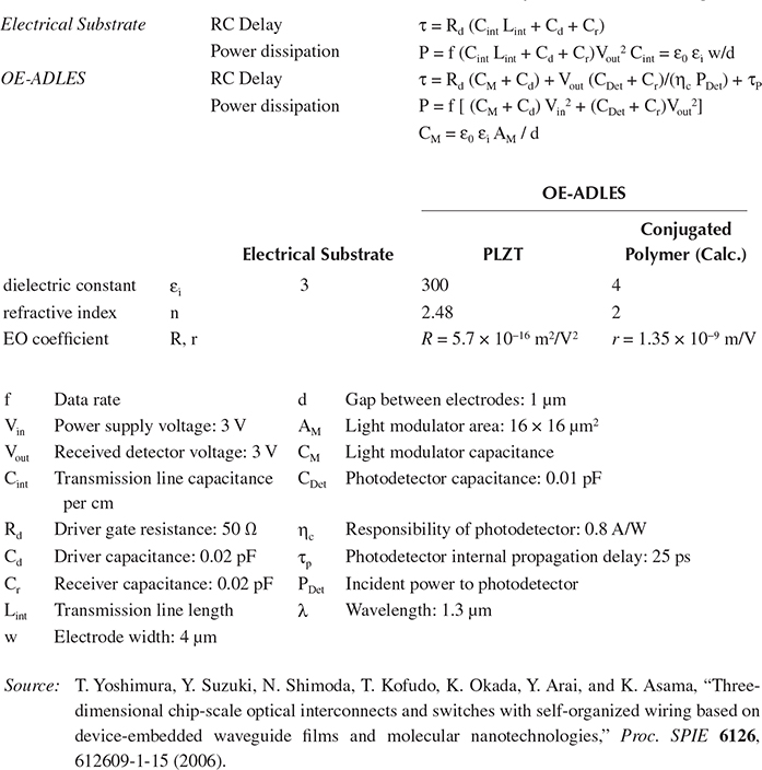
In order to estimate RC delay and power dissipation in OE-ADLES, the models shown in Figure 8.5 are considered [24,25]. For electrical substrates, data transmissions are treated as a process for charging up a buffer driver, a transmission line, and a receiver through a gate resistance of the buffer driver. For OE-ADLES, on the other hand, data transmissions are treated as a process for charging up a buffer driver and a light modulator through the gate resistance of the buffer driver, and a process for charging up a PD and a receiver by photocurrents generated in the PD. In Table 8.1, the formula for the RC delay and power dissipation are summarized as well as parameters for the calculations. Attenuation along the transmission lines is neglected. External power dissipation at light sources is not included. The waveguide prism deflector (WPD) optical switch described in Sections 6.1.2 and 6.1.3 is assumed as the light modulator for the transmitter.
In Figure 8.6, the delay and power dissipation of an electrical substrate and OE-ADLES are compared. Lead lanthanum zirconate titanate (PLZT) and the polymer MQD described in Sections 5.5 and 5.7 are assumed as EO materials for the WPD optical switch. For delay, OE-ADLES with the polymer MQD has an advantage over the electrical substrate in line length ranges longer than 1.2 cm for light power of 3 mW. With increasing light power introduced from external light sources, the response time becomes shorter, moving the break-even point toward shorter line length ranges of mm. For power dissipation, drastic reduction can be seen in OE-ADLES with the polymer MQD. The break-even point is located at line length of sub mm ranges. In OE-ADLES with PLZT, comparing with OE-ADLES with the polymer MQD, the break-even point is located at longer line length ranges for both delay and power dissipation.
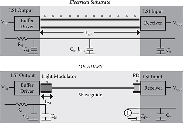
FIGURE 8.5 Models for estimation of RC delay and power dissipation in electrical interconnects and optical interconnects (OE-ADLES). From T. Yoshimura, Y. Suzuki, N. Shimoda, T. Kofudo, K. Okada, Y. Arai, and K. Asama, “Three-dimensional chip-scale optical interconnects and switches with self-organized wiring based on device-embedded waveguide films and molecular nanotechnologies,” Proc. SPIE 6126, 612609-1-15 (2006).
TABLE 8.1
Formula and parameters for calculations of rc Delay and power Dissipation
The superiority of optics is attributed to the capacitance reduction, that is, in the electrical substrate a large capacitance of the electrical transmission line exists, while in OE-ADLES, only small capacitances exist in the light modulators and PDs. As mentioned above, the polymer MQD exhibits faster responses and much lower power consumption compared with PLZT. The superiority of the polymer MQD comes from its small dielectric constant.
The key issue in OE-ADLES is availability of EO materials with a large EO coefficient and a small dielectric constant like the polymer MQD fabricated by the molecular layer deposition (MLD). Size reduction of the light modulators and PDs is another important issue. When they are miniaturized by one order of magnitude for each dimension, that is, the device thickness is reduced by one order of magnitude and the device area by two orders of magnitude, their capacitances as well as the internal propagation delay in PDs will be reduced by one order of magnitude in principle. This will move the break-even points to sub mm ranges.
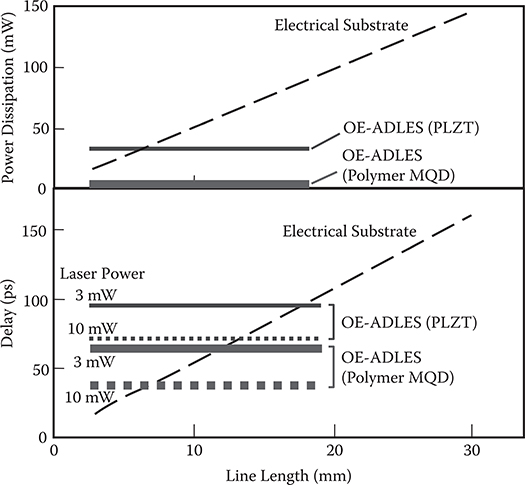
FIGURE 8.6 Comparisons of RC delay and power dissipation between electrical interconnects and optical interconnects (OE-ADSLES). From T. Yoshimura, Y. Suzuki, N. Shimoda, T. Kofudo, K. Okada, Y. Arai, and K. Asama, “Three-dimensional chip-scale optical interconnects and switches with self-organized wiring based on device-embedded waveguide films and molecular nanotechnologies,” Proc. SPIE 6126, 612609-1-15 (2006).
8.3 3-D Micro Optical Switching System (3D-MOSS)
The rapid increase in data rate and volume in networking and processing systems is promoting progress of massive optical switching [26]. This trend results in a key issue—miniaturization of high-speed massive optical switching systems. The miniaturization is useful for high-speed packet switching in optical communication systems and board-level reconfigurable optical interconnects.
In order to provide a solution for the issue, we proposed the three-dimensional micro optical switching system (3D-MOSS) based on S-FOLM, where OE films with embedded optical switches are stacked. 3D-MOSS will overcome speed limits of ~ms in micro-electromechanical systems (MEMS) and thermo-optics, to provide high-speed massive switching with large-scale integration of optical switches consisting of EO waveguides.
In the present section, 3D-MOSS structure is designed and the possible size and performance are theoretically predicted [7,27, 28 and 29] by the beam propagation method (BPM) and the finite difference time domain (FDTD) method. The impact of polymer MQD fabricated by MLD is also discussed.
8.3.1 The 3D-MOSS Concept
An example of 3D-MOSS configuration is shown in Figure 8.7(a) for a case involving a 32 × 32 Banyan network. It consists of five optical switch arrays, in which sixteen 2 × 2 optical switches are arranged in a 3-D optical network. The optical switch consists of EO waveguides that exhibit high-speed switching characteristics. The optical network is divided into four blocks—BL 1, 2, 3, and 4, which are stacked to make a four-layer structure. Between optical switch arrays, a connection area exists. Adjacent optical switch arrays i and i + 1 are connected by optical wiring in connection area i. Connection areas consisting of in-plane optical connections with in-plane waveguides and corner-turning micro reflectors are identified as “in-plane connection areas,” and those consisting of vertical optical connections with optical Z-connections, which are built from pairs of 45° reflectors and vertical waveguides for interplane links, are identified as “vertical connection areas.” In the model shown in Figure 8.7(a), connection areas 3, and 5 are in-plane connection areas, and connection areas 1 and 2 are vertical connection areas.
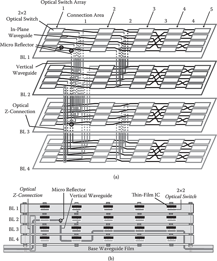
FIGURE 8.7 (a) An example of 3D-MOSS configuration for 32 × 32 switching. (b) A possible 3D-MOSS structure consisting of four layers. From T. Yoshimura, M. Ojima, Y. Arai, and K. Asama, “Three-dimensional self-organized micro optoelectronic systems for board-level reconfigurable optical interconnects: performance modeling and simulation,” IEEE J. Select. Topics in Quantum Electron. 9, 492–511 (2003).
The degree of three-dimensional characteristics of the networks is represented by D3D, which indicates the number of vertical connection areas in a 3D-MOSS. For example, in a conventional planar structure, D3D = 0. For 3D-MOSS with two layers, in which optical wiring in connection area 1 is carried out by vertical optical connections, D3D = 1. With increasing layer counts, D3D increases. In the 3D-MOSS shown in Figure 8.7(a), D3D = 2.
A possible 3D-MOSS structure is schematically illustrated in Figure 8.7(b). On a base waveguide film, OE films, in which optical switches (and driver ICs if necessary) are embedded together with optical waveguides, are stacked. The optical waveguides in the base waveguide film is connected to optical waveguides in the OE films by optical Z-connections similar to inter-OE-film connections. For example, an input light signal introduced into the 3D-MOSS from the base waveguide film is coupled to BL 2 through an optical Z-connection and is switched in the layer. The signal is coupled to BL 4 and is again switched, followed by transition to BL 3, and finally is output into the base waveguide film. 3D-MOSS has a potential for high-speed massive optical switching capability since it uses optical switches with EO waveguides.
A structural example of board-level reconfigurable optical interconnects with 3D-MOSS is shown in Figure 8.8. Thin-film VCSELs and PDs are embedded in an optical interconnect board by PL-Pack with SORT. LSIs are mounted on the board. For simplicity, interface films that should be inserted between the board and the LSIs are not drawn. When OE-ADLES is adopted, LSIs can be mounted on the board without the interface films. Instead of LSIs, 3D OE LSIs can also be used. For route switching between LSIs, 3D-MOSSs are mounted on the board. Figure 8.9 shows a possible example of 3-D reconfigurable optical interconnects built from multilayer OE boards, 3-D stacked OE MCM, and 3D-MOSSs.
8.3.2 IMPLEMENTATION OF SOLNET IN 3D-MOSSs
In optical packet switching systems, as well as in board-level reconfigurable optical interconnects, the channel count is quite large, resulting in a large number of optical coupling points. This forces us to align a lot of photonic devices precisely with enormous effort. Furthermore, in 3D-MOSS, vertical waveguides are necessary for interlayer connections. In order to achieve drastic cost reduction of the OE system, some technology to construct a 3-D optical network with a self-organized manner is required. One possible candidate is the self-organized 3-D optical circuits with SOLNET described in Section 7.4.
Figure 8.10 shows a concept for SOLNET implementation in 3-D optical circuits in S-FOLM. First, OE devices are arranged in a designed configuration in optical waveguide films to make OE films. The OE films are stacked to construct a 3-D structure. Next, by introducing some excitation to the 3-D structure from outside, self-aligned 3-D optical circuits of SOLNET are automatically constructed, including coupling optical paths between devices and optical Z-connections.
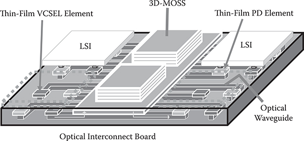
FIGURE 8.8 Structural example of board-level reconfigurable optical interconnects with 3D-MOSS. From T. Yoshimura, M. Ojima, Y. Arai, and K. Asama, “Three-dimensional self-organized micro optoelectronic systems for board-level reconfigurable optical interconnects: performance modeling and simulation,” IEEE J. Select. Topics in Quantum Electron. 9, 492–511 (2003).
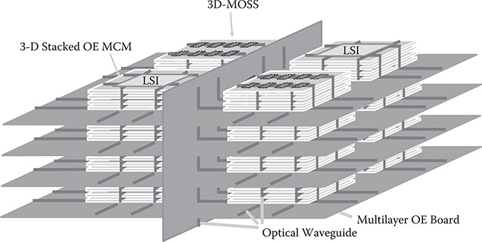
FIGURE 8.9 An example of 3-D reconfigurable optical interconnects built from multilayer OE boards, 3-D stacked OE MCMs, and 3D-MOSSs. From T. Yoshimura, Y. Suzuki, N. Shimoda, T. Kofudo, K. Okada, Y. Arai, and K. Asama, “Three-dimensional chip-scale optical interconnects and switches with self-organized wiring based on device-embedded waveguide films and molecular nanotechnologies,” Proc. SPIE 6126, 612609-1-15 (2006).
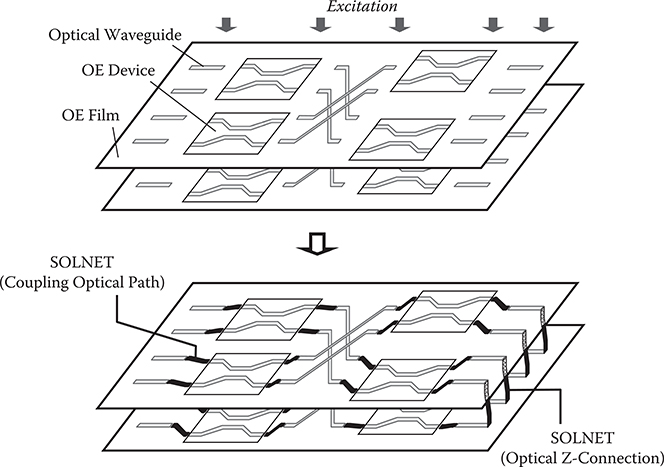
FIGURE 8.10 Concept of SOLNET implementation in 3-D optical circuits in S-FOLM. From T. Yoshimura, M. Ojima, Y. Arai, and K. Asama, “Three-dimensional self-organized micro optoelectronic systems for board-level reconfigurable optical interconnects: performance modeling and simulation,” IEEE J. Select. Topics in Quantum Electron. 9, 492–511 (2003).
In self-organized 3-D optical circuits, even if some misalignment of the optical waveguides and the stacked films exist, self-organized optical couplings can be achieved, which will reduce fabrication cost, especially the cost for assembly and optical Z-connection formation.
For SOLNET implementation in S-FOLM, write beam insertion is a serious concern. Because 3D-MOSS has a large number of connection parts and many of them are terminated by two optical switches, it is impossible to introduce write beams from outside. The problem can be resolved, as shown in Figure 8.11, by R-SOLNET and phosphor SOLNET, as described in Section 7.4.1. First, OE films are made by transferring optical switches onto final substrates using SORT. Before the transfer, wavelength filters, which can selectively reflect write beams of wavelengths typically between 0.35 μm and 0.7 μm and pass signal beams of 0.5–1.5 μm, are deposited just on core surfaces at the edge of optical switches using atomic layer deposition (ALD) and MLD with the assistance of photolithography.
Next, as Figure 8.11 shows, a preform is constructed by stacking the OE films. For write beam generation, phosphor is partially doped in optical waveguides. Photoinduced refractive index (PRI) materials are inserted in parts where optical wiring is necessary. Then, by illuminating the phosphor with UV light from outside the 3D-MOSS, write beams generated in the phosphor are introduced into the PRI materials through optical waveguides to make SOLNET. For vertical waveguide construction, the write beams are introduced into the PRI materials from upper and lower optical waveguides through 45° reflectors to form SOLNET. For connections between an in-plane waveguide and a waveguide within an optical switch, a write beam introduced into the PRI material from the in-plane waveguide is reflected by a wavelength filter on the waveguide core edge of the optical switch. The two write beams are attracted each other to construct a SOLNET. UV light from outside corresponds to the excitation shown in Figure 8.10. It should be noted that the same method is effective for VCSEL-waveguide and PD-waveguide couplings in optical interconnect boards by depositing the wavelength filters on the active regions of VCSELs and PDs.
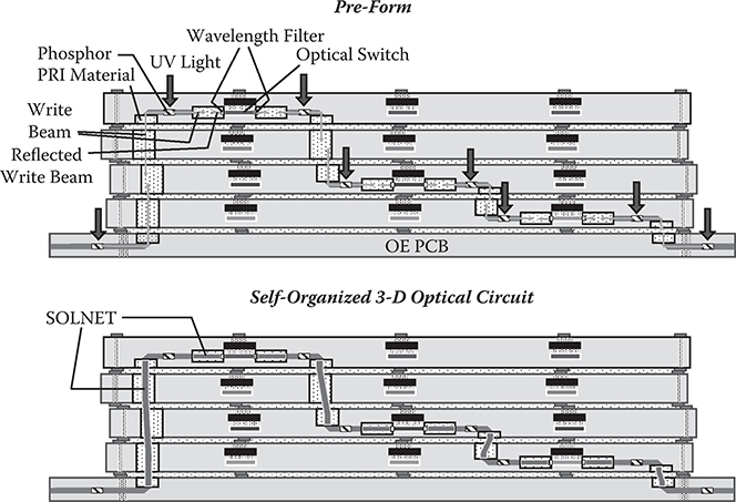
FIGURE 8.11 Fabrication process of self-organized 3-D optical circuits. From T. Yoshimura, M. Ojima, Y. Arai, and K. Asama, “Three-dimensional self-organized micro optoelectronic systems for board-level reconfigurable optical interconnects: performance modeling and simulation,” IEEE J. Select. Topics in Quantum Electron. 9, 492–511 (2003).
8.3.3 STRUCTURAL MODEL OF 3D-MOSS
In Table 8.2, parameters for the 1024 × 1024 3D-MOSS model are summarized. The 3-D optical circuit backbone consists of optical waveguides with a core cross-section of 4 × 4 µm2, core refractive index nCore of 1.52, and clad refractive index nClad of 1.50.
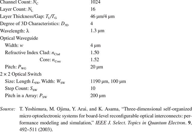
Figure 8.12 shows top-view illustrations of Banyan network models for a conventional planar structure and a 3D-MOSS structure. Channel count is NC, meaning NC × NC switching is considered. In the present model, NC is 1024. The network consists of 2 × 2 optical switch arrays, which are connected by optical waveguides in connection areas. The optical switch is the WPD optical switch shown in Figure 6.19. Although the PLZT thickness is 400 nm in Figure 6.19, in the present calculation the PLZT thickness is assumed to be 4 µm in order to match the PLZT thickness to core thickness of the 3-D optical circuit backbone. In this case, switching voltage is 12 V. One array contains NC/2 2 × 2 optical switches with length LSW of 1190 µm and width WSW of 100 µm. The length of the array equals the individual switch length LSW. The optical switch array count is SSW, which is 10 in the present model.
TABLE 8.2
parameters for the 1024 × 1024 3D-moSS model
In 3D-MOSS, the network is divided into NL blocks, which are stacked to make an NL-layer 3-D structure. The general expression for 3-D characteristics of networks, D3D, is given as follows.
Optical wiring is carried out by vertical optical connections in connection areas 1 to D3D, and in-plane optical connections in connection areas D3D + 1 to SSW − 1.
It is found from Figure 8.12 that the area of the network is drastically reduced in 3D-MOSS, when compared with the conventional planar structure. The sizes inserted in Figure 8.12, as well as in Figures 8.13 through 8.15, are calculated using the general Equations (8.2)–(8.6) described later.
Figure 8.13 shows a side-view illustration of 3D-MOSS. Since (8.1) gives D3D = 4 for the present model with NL = 16, vertical optical connections are in connection areas 1–4, and in-plane optical connections in connection areas 5–9. The region that includes connection areas 5–9 corresponds to the 64 × 64 Banyan network with a conventional planar structure shown in Figure 8.14. TL and TG are the layer thickness and gap thickness, respectively. In the present model, TL is 46 µm and TG is 4 µm. Thickness per one layer is 50 µm.
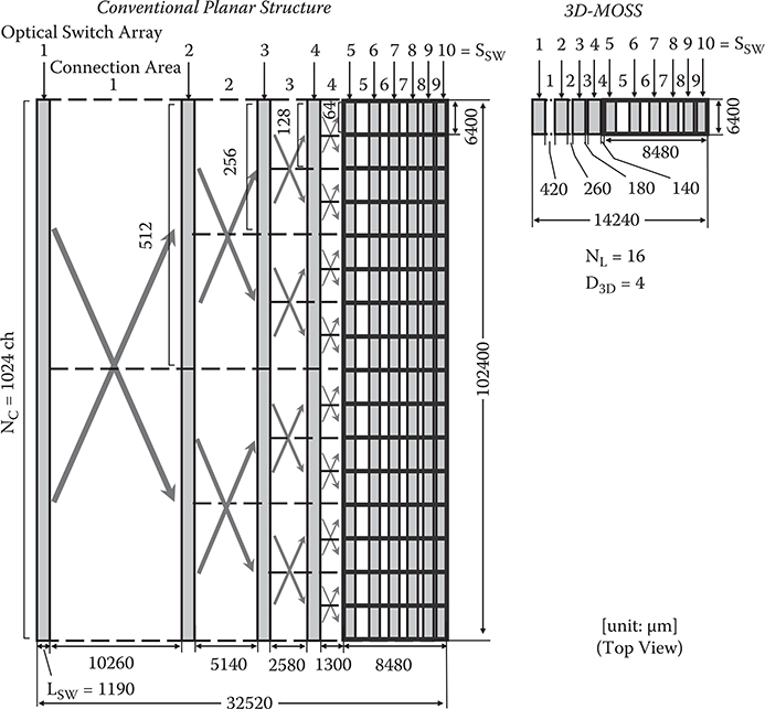
FIGURE 8.12 Top-view illustrations of Banyan network models for a conventional planar structure and a 3D-MOSS structure. From T. Yoshimura, M. Ojima, Y. Arai, and K. Asama, “Three-dimensional self-organized micro optoelectronic systems for board-level reconfigurable optical interconnects: performance modeling and simulation,” IEEE J. Select. Topics in Quantum Electron. 9, 492–511 (2003).
As an example of in-plane connection area, detail of connection area 5 is shown in Figure 8.15(a). Connections between optical switch arrays are constructed by crank-shaped waveguides consisting of a pair of corner-turning micro reflectors. PSW and PWG are the pitch of the optical switches and the pitch of the optical waveguides, respectively. Interswitch connection line count is expressed by Nc / 25 for connection area 5. Then, by adding PWG for buffer spaces, the length of connection area 5 is given by (Nc / 25 + 1) PWG. The width is given by ((Nc / 2) / 2D3D)PSW. Thus, the expressions for connection area length and width of in-plane connection area i can be generalized as follows.
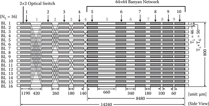
FIGURE 8.13 Side view illustration of Banyan network model for a 3D-MOSS structure with layer count NL = 16. From T. Yoshimura, M. Ojima, Y. Arai, and K. Asama, “Three-dimensional self-organized micro optoelectronic systems for board-level reconfigurable optical interconnects: performance modeling and simulation,” IEEE J. Select. Topics in Quantum Electron. 9, 492–511 (2003).
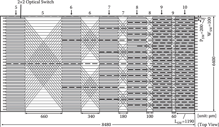
FIGURE 8.14 Top view illustration of 64 × 64 Banyan network with in-pane optical connections. From T. Yoshimura, M. Ojima, Y. Arai, and K. Asama, “Three-dimensional self-organized micro optoelectronic systems for board-level reconfigurable optical interconnects: performance modeling and simulation,” IEEE J. Select. Topics in Quantum Electron. 9, 492–511 (2003).
In the present model, PSW = 200 µm and PWG = 20 µm. PWG of 20 µm is wide enough for parallel wiring with a length of 1 cm to keep cross-talk below −30 dB for the assumed 4-µm-wide waveguides and 1.3-µm wavelength. By substituting the parameters into Equations (8.2) and (8.3), the size of connection area 5 can be calculated to be 660-µm long and 6400-µm wide. Similarly, the sizes for i = 6~9 can be calculated as shown in Figures 8.13 and 8.14.
As an example of a vertical connection area, a detailed side view of connection area 1 and a top view of a part of the connection area in BL 12 are shown in Figure 8.15(b). The interswitch connection line count in a cross-section is expressed as NL / 21−1 for connection area 1. Then, adding buffer spaces of 3PWG for corner-turning micro reflectors at the front and tail ends of the connection area, the length of connection area 1 is calculated to be (NL / 21−1 + 5)PWG. The width is the same as in the in-plane optical connection case. The height is NL(TL + GL). Thus, the expressions for connection area length L (V), width W (V), and height H (V) of vertical connection area i can be generalized as follows.
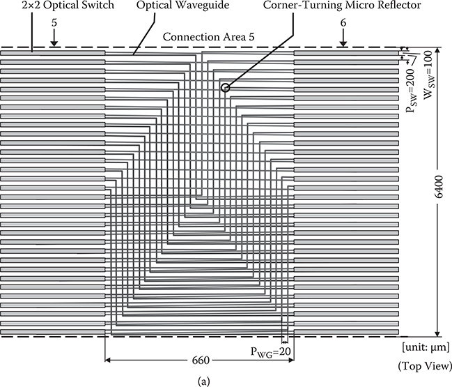
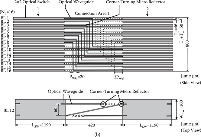
FIGURE 8.15 Details of (a) top view of connection area 5 and (b) side view of connection area 1 and top view of a part of the connection area in BL 12. From T. Yoshimura, M. Ojima, Y. Arai, and K. Asama, “Three-dimensional self-organized micro optoelectronic systems for board-level reconfigurable optical interconnects: performance modeling and simulation,” IEEE J. Select. Topics in Quantum Electron. 9, 492–511 (2003).
Parameter substitution into Equations (8.4), (8.5), and (8.6) gives the size of connection area 1 of 420 µm in length, 6400 µm in width, and 800 µm in height. Similarly, the sizes for i = 2~4 can be calculated as shown in Figures 8.12 and 8.13.
8.3.4 Optical Z-Connections and Optical Switches
8.3.4.1 Optical Z-Connections
Figure 8.16 shows an optical Z-connection model. Waveguides that are 4 µm wide are in the upper and lower layers. The gap between the waveguides of the adjacent layers is 16 µm. The waveguides are connected by two 45° reflectors and a vertical waveguide that is 4 µm wide. The reflectors can be metal mirrors, dielectric multilayer wavelength filters, gratings, or photonic crystals. In the present work, metal mirrors with a refractive index of 0.4 for the real part and −5 for the imaginary part are assumed. Analysis is performed by the BPM/FDTD method coupled simulation. It can be seen in Figure 8.16 that the propagating light beam smoothly propagates from the upper layer to the lower layer through optical Z-connection with little mode disturbance with respect to intensity. Calculated loss of the optical Z-connection (γz) is 0.97 dB. The loss is basically induced at the mirror reflection parts.
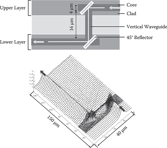
FIGURE 8.16 Optical Z-connection model with 4-µm-wide waveguides. From T. Yoshimura, M. Ojima, Y. Arai, and K. Asama, “Three-dimensional self-organized micro optoelectronic systems for board-level reconfigurable optical interconnects: performance modeling and simulation,” IEEE J. Select. Topics in Quantum Electron. 9, 492–511 (2003).
8.3.4.2 Optical Switches
Optical switches for 3D-MOSS should be small and exhibit high speed and low cross-talk characteristics. At the same time, the switches should be stable against thermal and dimensional fluctuations since a large number of optical switches are involved in 3D-MOSS, say, 5120 2 × 2 switches in 1024 × 1024 Banyan network. This implies that flux-controlled switches are preferable to phase-controlled switches, giving us digital optical switches, internal total reflection switches, variable well optical ICs (VWOICs), and WPD optical switches as candidates. In the present simulation, we selected the WPD optical switches consisting of PLZT as mentioned in Section 8.3.3.
8.3.5 PREDICTED PERFORMANCE OF 3D-MOSS
Figure 8.17 shows a schematic illustration of a 3-D MOSS calculation model, where only a part of the model is drawn for simplicity. OE films are placed with a pitch of TL + TG. In OE films, 2 × 2 WPD optical switches of length LSW and width WSW are arranged with a pitch of PSW. Intralayer wiring is carried out by in-plane waveguides with a pitch of PWG while interlayer wiring is by optical Z-connections. Major losses caused in 3D-MOSS are indicated by γ in the figure. γP is propagation loss of optical waveguides, γCR is loss induced at a right-angle waveguide–waveguide cross point, γZ is loss of an optical Z-connection, γCT is loss of a pair of corner turnings with two mirrors, γG is loss at a layer gap, γSW is loss within a 2 × 2 optical switch, and γW−S is waveguide-switch coupling loss.
Predicted system performance of 1024 × 1024 3D-MOSS is summarized in Table 8.3 as well as those of conventional planar structures for comparison. The process to derive performance is described below.
8.3.5.1 Size and insertion loss
For 3D-MOSS with SSW and D3D, connection areas 1 to D3D have vertical optical connections while connection areas D3D + 1 to SSW − 1 have in-plane optical connections. The connection area length for the in-plane connection areas and the vertical connection areas are respectively expressed by Equations (8.2) and (8.4), and the width by Equations (8.3) and (8.5). Therefore, total 3D-MOSS length L3D-MOSS, width
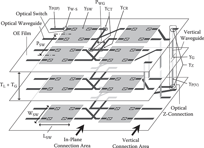
FIGURE 8.17 A schematic illustration of a 3-D MOSS model for insertion loss calculations. From T. Yoshimura, Y. Arai, H. Kurokawa, and K. Asama, “Predicted insertion loss reduction achieved by implementing three-dimensional microoptical network in chip-scale optical interconnects,” IEEE Photon. Technol. Lett. 16, 647–649 (2004).
TABLE 8.3
Summary of predicted System performance of 1024 × 1024 3D-moSS with D3D = 4
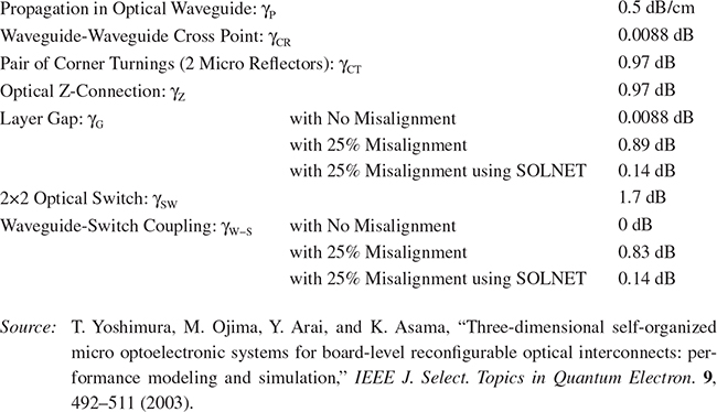
Major losses in 3D-MOSS are listed in Table 8.4. Propagation loss γP of optical waveguides is assumed to be 0.5 dB/cm, which is typical in fluorinated polyimide. Loss induced at a right-angle waveguide–waveguide cross point γCR is estimated by the beam propagation method (BPM) simulation to be 0.0088 dB. Loss of an optical Z-connection γZ of 0.97 dB was calculated in Section 8.3.4. Since a pair of corner turnings with two mirrors has the same structure as the optical Z-connection, the loss γCT can also be 0.97 dB. A cross point of a vertical waveguide and a layer gap of 4 µm can be regarded as a kind of right-angle waveguide–waveguide cross point. So, loss at a layer gap γG is estimated to be 0.0088 dB. BPM calculation reveals that γG with 25% misalignment is 0.89 dB, and γG with 25% misalignment is 0.14 dB when SOLNET is used for the coupling. Loss within a 2 × 2 optical switch γSW was estimated to be 1.7 dB in Section 6.1.3. Waveguide-switch coupling loss γW−S is basically 0 dB for no misalignment. For the case with 25% misalignment, the BPM calculation reveals that γW−S is 0.83 dB. For SOLNET coupling with 25% misalignment, similar to the case of γG, γW−S is 0.14 dB. In the present simulation, boundary reflection losses are neglected, assuming an antireflective (AR) coating on the edge surfaces of individual parts.
TABLE 8.4
Major Losses in 3D-MOSS
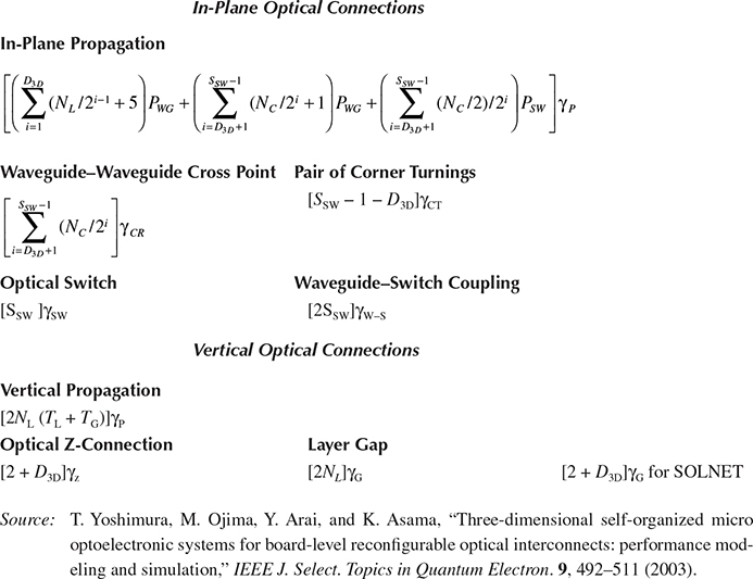
General expressions for eight kinds of losses in 3D-MOSS are derived in terms of the major losses listed in Table 8.4. The results are summarized in Table 8.5. In-plane optical connections include in-plane propagation, waveguide–waveguide cross points, pairs of corner turnings, optical switches, and waveguide–switch couplings. Vertical optical connections include vertical propagation, optical Z-connections, and layer gaps.
For total loss due to in-plane propagation, the first and the second terms are caused by the horizontal line length given by the second and the third terms of Equation (8.7). The third term is caused from line length perpendicular to the horizontal direction. Since lines in vertical connection areas have no contribution to the line length perpendicular to the horizontal direction basically, the summation is carried out only for the in-plane connection areas. For total loss due to waveguide–waveguide cross points, as shown in Figure 8.15(a), an optical waveguide has a cross-point count of NC/2i in in-plane connection area i. In vertical connection areas, no waveguide cross points exist. Thus, the summation for the total loss calculation is carried out for the in-plane connection areas. Total loss due to corner turnings is determined by the number of pair of corner turnings that equals the in-plane connection area count since optical signals experience one pair of corner turnings in one in-plane connection area. Total loss within optical switches and total loss at waveguide–switch coupling points are respectively induced by SSW optical switches and 2 SSW waveguide–switch coupling points. For vertical propagation, as can be seen from Figure 8.13 and Figure 8.15(b), the total loss is determined by the optical path length that corresponds to two times the 3D-MOSS thickness. Since optical signals experience one optical Z-connection in one vertical connection area as shown in Figure 8.15(b), total loss caused by optical Z-connections, with adding two optical Z-connections for input and output, is calculated to be [2 + D3D]γZ. Total loss due to layer gaps is determined by two times the layer gap count contained in a 3D-MOSS. When a SOLNET is implemented in vertical optical connections, total loss due to layer gaps is replaced with a product of total Z-connection count times γG for the SOLNET.
TABLE 8.5
General Expressions for Losses in 3D-MOSS
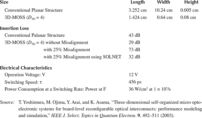
By substituting the parameters in Table 8.2 into Equations (8.7), (8.8), and (8.9), length, width, and height of 3D-MOSS can be respectively calculated to be 1.424 cm, 0.64 cm, and 0.08 cm as shown in Table 8.3. For conventional planar structures, the length is 3.252 cm, the width is 10.24 cm, and the height is 0.005 cm. Therefore, it is found that drastic occupation area reduction of 3/100 is achieved in 3D-MOSS with D3D = 4. Insertion losses of 3D-MOSS, shown in Table 8.3, can be obtained by summation of the eight losses listed in Table 8.5. While insertion loss of the conventional planar structure is 43 dB, that of the 3D-MOSS is 29 dB, indicating that a 14-dB loss reduction is achieved in 3D-MOSS. In Figure 8.18, occupation areas and insertion losses of 3D-MOSS are shown as a function of D3D [30]. D3D = 0 implies conventional structure, and D3D = 9 implies that all the connection areas consist of vertical optical connections. It is found that the occupation area decreases drastically with D3D. Insertion loss, on the other hand, has a peak in the region of D3D = 4~6. For small D3D, the main contribution to the loss is waveguide–waveguide cross points while layer gaps for large D3D. The results indicate that size and loss of 3D-MOSS can be optimized by selecting D3D.
The misalignment issue is a serious concern in 3D-MOSS. As shown in Table 8.4, misalignment between adjacent layers causes a layer gap loss γG of 0.89 dB. At a waveguide–switch coupling, which is equivalent to a coupling between 4-µm-wide waveguides, 25% misalignment induces a loss γW−S of 0.83 dB. By substituting these loss values into the summation of the eight losses shown in Table 8.5, insertion loss of 3D-MOSS with 25% misalignment is estimated to be 73 dB as shown in Table 8.3. In this case, in order to transmit optical signals with reasonable power, three times optical amplification might be required in 3D-MOSS as a result of inserting amplifier layers. As can be seen in Figure 8.18, SOLNET implementation is effective to reduce the insertion loss. By using γG and γW−S of 0.14 dB listed in Table 8.4 for 25% misalignment using SOLNET, the insertion loss of the SOLNET-implemented 3D-MOSS is calculated to be 32 dB, which is close to the loss in 3D-MOSS without misalignment.
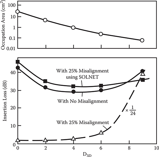
FIGURE 8.18 D3D dependence of occupation areas and insertion losses of 3D-MOSS. From T. Yoshimura, Y. Arai, H. Kurokawa, and K. Asama, “Predicted insertion loss reduction achieved by implementing three-dimensional microoptical network in chip-scale optical interconnects,” IEEE Photon. Technol. Lett. 16, 647–649 (2004).
It was reported that high-accuracy bonding equipment enables layer stacking with positional accuracy of 1 µm for 1-cm2 chips [31]. Therefore, for 3D-MOSS of 1.424 cm × 0.64 cm, it is consistent to assume maximum positional misalignment of ~1 µm, which corresponds to 25% misalignment for optical circuit backbones consisting of optical waveguides with 4 × 4-µm2 core cross-sections. The insertion loss of 32 dB for 1024 × 1024 SOLNET-implemented 3D-MOSS is still high, which requires an optical amplifier layer insertion or 10 mW-order input light signals. For further simplification of the system, each loss listed in Table 8.4 should be decreased by optimizing individual structures and materials.
8.3.5.2 electrical characteristics
Switching speed and power consumption can be estimated based on the charge-discharge model for the prism-shaped capacitor in the waveguide prism deflector. The WPD optical switch model used in the present calculation is the same as the model shown in Figure 6.19 except that the PLZT thickness is increased from 400 nm to 4 µm and the applied voltage is increased from 1.2 V to 12V. Therefore, the capacitance C, switching speed τ, and power consumption Power that are given by Equations (6.9), (6.8), and (6.10) for one prism-shaped capacitor are respectively calculated to be 0.57 pF, 57 ps for driver on-resistivity RON = 100 Ω, and 41 mW at F = 5 × 10⁸ 1/s.
When the number of the waveguide prism deflectors in a WPD optical switch is NPrism, switching speed τ for RON is given by
For power consumption, total WPD optical switch count in a 3D-MOSS is (NC / 2)SSW, giving NPrism (NC / 2)SSW for the total count of the prism-shaped capacitors contained in a 3D-MOSS. Then, total capacitance arising from the deflectors is given by C NPrism (NC / 2)SSW. As a result, power consumption at a switching rate of F in a 3D-MOSS is expressed as follows:
By substituting C = 0.57 pF, V = 12 V, NPrism = 8, Nc = 1024, and SSW = 10 into Equations (8.10) and (8.11), τ = 456 ps for RON = 100 Ω, and Power = 33 W for F = 1 × 10⁷ 1/s are obtained. The power consumption of 33 W corresponds to a power density of 36 W/cm2 since the area of the 3D-MOSS model is 1.42 × 0.64 cm2. This value is comparable to acceptable heat generation of 30 W/cm2 reported by K. Takahashi [31] for stacked LSI of 1-cm2 area. These results are included in Table 8.3.
8.3.6 Impact of Nano-Scale Waveguides and Polymer MQDs On 3D-MOSS Performance
When high-index contrast (HIC) nano-scale waveguides having 400 × 400 nm2 core cross-sections are used for the 3-D optical circuit backbone in the 3D-MOSS, the PLZT thickness, that is, the electrode gap in the WPD optical switches, can be reduced to 400 nm. In this case, switching voltage is reduced to 1.2 V to achieve low-voltage switching, which is favorable for low-power and high-speed operation. The HIC-waveguide-based optical circuits can be fabricated by PRI sol-gel materials as described in Section 7.3.
Figure 8.19 shows switching rate dependence of power density generated in 3D-MOSS for various EO materials of a WPD optical switch. Power density increases with switching rate. Possible switching rate is determined by a balance of heat generation and releasing rates in 3D-MOSS. For a given heat releasing rate, the lower the heat generation rate becomes, the higher the available switching rate becomes as far as switching speed of WPD optical switch τ is sufficiently fast. The power density versus switching rate relationship varies depending on EO materials. In PLZT, the switching rate is limited below 1 × 10⁷ 1/s when the limit of the heat releasing capability is 30 W/cm2. In the styrylpyridinium cyanine dye (SPCD) organic crystal, which has an EO coefficient of 430 pm/V, an expected dielectric constant of ~4ε0 and a refractive index of 1.55 as mentioned in Section 7.1.2, the line moves to the right-hand side, indicating that higher switching rates are expected than in PLZT.
Drastic switching rate improvement is expected in polymer MQDs [32, 33 and 34], which has a potential EO coefficient of ~1000 pm/V, dielectric constant of ~4ε0, and refractive index of ~2, resulting in a possible switching rate around 1010 1/s.
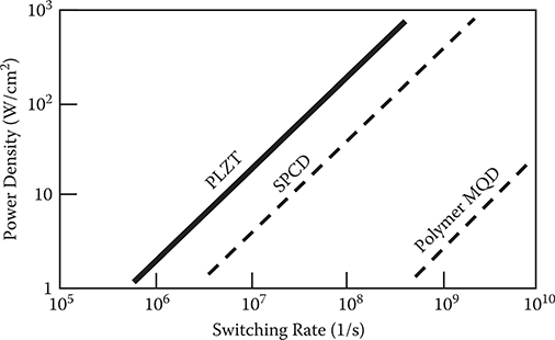
FIGURE 8.19 Switching rate dependence of power density generated in 3D-MOSS for various EO materials of a WPD optical switch. From T. Yoshimura, M. Ojima, Y. Arai, and K. Asama, “Three-dimensional self-organized micro optoelectronic systems for board-level reconfigurable optical interconnects: performance modeling and simulation,” IEEE J. Select. Topics in Quantum Electron. 9, 492–511 (2003).
These results of performance simulation indicate that 1024 × 1024 3D-MOSS is viable for massive optical packet switching systems and board-level reconfigurable optical interconnects from the perspective of size, insertion loss, switching speed, and thermal management. It is also suggested that the polymer MQD fabricated by MLD as well as the nano-scale waveguides will have a significant impact on high-speed massive optical switching systems.
References
1. T. Yoshimura, J. Roman, Y. Takahashi, M. Lee, B. Chou, S. Beilin, W. Wang, and M. Inao, “Optoelectronic scalable substrates based on film/Z-connection and its application to film optical link module (FOLM),” Proc. SPIE 3952, from Photonics West 2000, San Jose, California, 202–213 (2000).
2. T. Yoshimura, J. Roman, Y. Takahashi, M. Lee, B. Chou, S. I. Beilin, W. V. Wang, and M. Inao, “Proposal of optoelectronic substrate with Film/Z-connection based on OE-film,” Proc. 3rd IEMT/IMC Symposium, 140–145 (1999).
3. T. Yoshimura, Y. Takahashi, M. Inao, M. Lee, W. Chou, S. Beilin, W.C. Wang, J. Roman, and T. Massingill, Three-dimensional opto-electronic modules with electrical and optical interconnections and methods for making, U.S. Patent 6,690,845 (2004).
4. T. Yoshimura, Y. Takahashi, M. Inao, M. Lee, W. Chou, S. Beilin, W.C. Wang, J. Roman, and T. Massingill, Multi-layer opto-electronic substrates with electrical and optical interconnections and methods for making, U.S. Patent 6,845,184 (2005).
5. T. Yoshimura, J. Roman, Y. Takahashi, W. V. Wang, M. Inao, T. Ishitsuka, K. Tsukamoto, K. Motoyoshi, and W. Sotoyama, “Self-organizing waveguide coupling method “SOLNET” and its application to film optical circuit substrates,” Proc. 50th Electronic Components & Technology Conference (ECTC), Las Vegas, Nevada, 962–969 (2000).
6. T. Yoshimura, T. Inoguchi, T. Yamamoto, S. Moriya, Y. Teramoto, Y. Arai, T. Namiki, and K. Asama, “Self-organized lightwave network based on waveguide films for three-dimensional optical wiring within boxes,” J. Lightwave Technol. 22, 2091–2100 (2004).
7. T. Yoshimura, M. Ojima, Y. Arai, and K. Asama, “Three-dimensional self-organized micro optoelectronic systems for board-level reconfigurable optical interconnects: performance modeling and simulation,” IEEE J. Select. Topics in Quantum Electron. 9, 492–511 (2003).
8. T. Yoshimura and Y. Arai, 3D optoelectronic micro system, U.S. Patent 2006/0261432 (2006).
9. T. Yoshimura, “Proposed applications of 3-D optical interconnect technologies to integrated chemical systems,” 2007 Digest of the LEOS Summer Topical Meetings [Bio-Inspired Sensors and Application/Imprinting on Photonic Integrated Circuits], Portland, Oregon, 129–130 (2007).
10. T. Yoshimura, K. Ogushi, Y. Kitabayashi, K. Naito, Y. Miyamoto, and M. Miyazaki, “Optical waveguide films with two-layer skirt-type core end facets for beam leakage reduction at 45° mirrors,” Proc. SPIE 6899, from Photonics West 2008, San Jose, California, 689913- 1-11 (2008).
11. T. Yoshimura, Integrated photonic/electronic/chemical systems, solar energy conversion systems, light collectors, and optical waveguides, Japanese Patent Tokukai 2009-4717 (2009) [in Japanese].
12. T. Yoshimura and K. Asama, Integrated chemical systems and integrated light energy conversion systems, Japanese Patent Tokukai 2007-107085 (2007) [in Japanese].
13. T. Yoshimura, Molecular nano systems: Applications to optoelectronic computers and solar energy conversion, Corona Publishing Co., Ltd., Tokyo (2007) [in Japanese].
14. D. A. B. Miller, “How large a system can we build without optics?” Workshop Notes, 8th Annual Workshop on Interconnections Within High Speed Digital Systems, Santa Fe, New Mexico, Lecture 1.2 (1997).
15. N. M. Jokerst, M. A. Brooke, S. Cho, S. ilkinson, M. Vrazel, S. Fike, J. Tabler, Y. J. Joo, S. Seo, D. S. Wils, and A. Brown, “The heterogeneous integration of optical interconnections into integrated microsystems,” IEEE J. Select. Topics in Quantum Electron. 9, 350–360 (2003).
16. C. Choi, L. Lin, Y. Liu, J. Choi, L. Wang, D. Haas, J. Magera, and R. T. Chen, “Flexible optical waveguide film fabrications and optoelectronic devices integration for fully embedded board-level optical interconnects,” J. Lightwave Technol. 22, 2168–2176 (2004).
17. H. Takahara, “Optoelectronic multichip module packaging technologies and optical input/output interface chip-level packages for the next generation of hardware systems,” IEEE J. Select. Topics in Quantum Electron. 9, 443–451 (2003).
18. T. Mikawa, M. Kinoshita, K. Hiruma, T. Ishitsuka, M. Okabe, S. Hiramatsu, H. Furuyama, T. Matsui, K. Kumai, O. Ibaragi, and M. Bonkohara, “Implementation of active interposer for high-speed and low-cost chip level optical interconnects,” IEEE J. Select. Topics in Quantum Electron. 9, 452–459 (2003).
19. B. S. Rho, S. Kang, H. S. Cho, H.H. Park, S.W. Ha, and B.H. Rhee, “PCB-Compatible optical interconnection using 45°-ended connection rods and via-holed waveguides,” J. Lightwave Technol. 22, 2128–2134 (2004).
20. C. Berger, B. Offrein, and M. Schmatz, “Challenges for the introduction of board-level optical interconnect technology into product development roadmaps,” Proc. SPIE 6124, 61240J-1-12 (2006).
21. E.H. Lee, S. G. Lee, B. H. O, S. G. Park, and K. H. Kim, “Fabrication of a hybrid electrical-optical printed circuit board (EO-PCB) by lamination of an optical printed circuit board (O-PCB) and an electrical printed circuit board (E-PCB),” Proc. SPIE 6126, 61260L-1-10 (2006).
22. A. Glebov, M. G. Lee, D. Kudzuma, J. Roman, M. Peters, L. Huang, and S. Zhou, “Integrated waveguide microoptic elements for 3D routing in board-level optical interconnects,” Proc. SPIE 6126, 61260L-1-10 (2006).
23. T. Yoshimura, J. Roman, Y. Takahashi, S. Beilin, W. Wang, and M. Inao, 4th International Conference on Organic Nonlinear Optics (ICONO’4), Extended Abstracts, Chitose, Japan, 278 (1998).
24. T. Yoshimura, J. Roman, Y. Takahashi, S. I. Beilin, W. V. Wang, and M. Inao, “Optoelectronic amplifier/driver-less substrate <OE-ADLES> for polymer-waveguide-based board-level interconnection: calculation of delay and power dissipation,” Nonlinear Optics 22, 453–456 (1999).
25. T. Yoshimura, Y. Suzuki, N. Shimoda, T. Kofudo, K. Okada, Y. Arai, and K. Asama, “Three-dimensional chip-scale optical interconnects and switches with self-organized wiring based on device-embedded waveguide films and molecular nanotechnologies,” Proc. SPIE 6126, from Photonics West 2006, San Jose, California, 612609- 1-15 (2006).
26. M. W. Haney and M. P. Christensen, “Sliding banyan network,” J. Lightwave Technol. 14, 703–710 (1996).
27. T. Yoshimura, A. Hori, Y. Yoshida, Y. Arai, H. Kurokawa, T. Namiki, and K. Asama, “Coupling efficiencies in reflective self-organized lightwave network (R-SOLNET) simulated by the beam propagation method,” IEEE Photon. Technol. Lett. 17, 1653–1655 (2005).
28. T. Yoshimura, S. Tsukada, S. Kawakami, M. Ninomiya, Y. Arai, H. Kurokawa, and K. Asama, “Three-dimensional micro-optical switching system architecture using slab-waveguide-based micro-optical switches,” Opt. Eng. 42, 439–446 (2003).
29. T. Yoshimura, S. Tsukada, S. Kawakami, Y. Arai, H. Kurokawa, and K. Asama,, “3D micro optical switching system (3D-MOSS) architecture,” Proc. SPIE 4653, from Photonics West 2002, San Jose, California, 62–70 (2002).
30. T. Yoshimura, Y. Arai, H. Kurokawa, and K. Asama, “Predicted insertion loss reduction achieved by implementing three-dimensional microoptical network in chip-scale optical interconnects,” IEEE Photon. Technol. Lett. 16, 647–649 (2004).
31. K. Takahashi, “Research and development on ultra-high-density 3-dimensional LSI-chip-stack packaging technologies,” The 3rd Annual Meeting on Electronics System Integration Technologies Digest, edited and published by the Electronic System Integration Technology Research Department, Association of Super-Advanced Electronics Technologies (ASET), 43–94 (2002).
32. T. Yoshimura, “Enhancing second-order nonlinear optical properties by controlling the wave function in one-dimensional conjugated molecules,” Phys. Rev. B40, 6292–6298 (1989).
33. T. Yoshimura, “Theoretically predicted influence of donors and acceptors on quadratic hyperpolarizabilities in conjugated long-chain molecules,” Appl. Phys. Lett. 55, 534–536 (1989).
34. T. Yoshimura, “Design of organic nonlinear optical materials for electro-optic and all-optical devices by computer simulation,” FUJITSU Sc. Tech. J. 27, 115–131 (1991).