
Three-Dimensional ICs with Inductive Links*
Abstract
An alternative approach to through silicon vias (TSVs) for intertier communication is contactless interconnects. State-of-the-art techniques to enable contactless communication through inductive links are described in this chapter. A comparison between TSV and inductive links in terms of performance and area constraints is provided. The effect of data multiplexing on the bandwidth of inductive links is described. Design issues for the on-chip inductors are discussed. Models of crosstalk noise from the inductive links to adjacent interconnects are presented. Furthermore, measures to avoid interference for specific types of interconnects are provided. A multiobjective algorithm for the design of inductive links to support intertier communication is also described.
Keywords
AC coupling; inductive links; contactless intertier communication; crosstalk noise; on-chip inductors
Wireless intertier communication enables new opportunities in three-dimensional (3-D) integrated circuits. Contactless interfaces based on inductive or capacitive coupling have been proposed as substitutes for through silicon vias (TSVs) and microbumps, as discussed in Chapter 3, Manufacturing Technologies for Three-Dimensional Integrated Circuits. Using a wireless intertier communication scheme, the development of multifunctional, heterogeneous 3-D systems is enhanced. Disparate technologies can be seamlessly combined within the same package without requiring elaborate level shifting circuitry and electrostatic discharge protection required by galvanic interconnects.
Moreover, wireless interchip communication employs passive elements within each tier of a 3-D stack, which in turn can be manufactured using conventional two-dimensional (2-D) processes. Consequently, there is no need for additional masks that increase fabrication costs as compared with TSV manufacturing where additional processing steps, such as TSV etching and copper filling, are required [256]. As a result, wireless schemes provide inexpensive communication and possibly exhibit higher yield as compared to wired schemes. The basic features of wireless intertier communication schemes are presented in Section 6.1. The design of the on-chip inductors for intertier communication is discussed in Section 6.2, while the supporting circuitry for signal transmission and recovery are presented in Section 6.3. Challenges related to the design of the inductive links are considered in Section 6.4. Issues related to wireless power transfer across the tiers of a 3-D integrated system are briefly reviewed in Section 6.5. A short summary is provided in Section 6.6.
6.1 Wireless On-Chip Communication Interfaces
Wireless intertier communication, also termed AC coupling, is based on either capacitive or inductive links. Capacitive coupling uses the electric field formed between the two electrodes of a capacitor to communicate, where each electrode lies on a separate tier within a 3-D system. Alternatively, inductive links manipulate the magnetic flux between concentrically placed inductors on different tiers. Due to the superior performance of inductive links as compared to capacitive communication, only inductive coupling is discussed in this chapter. The advantages and limitations of wireless communication along with an overview of the inductive coupling operation are described in the following subsection.
6.1.1 Inductive Links
The most versatile of the wireless on-chip communication schemes are inductively driven interfaces. Inductive links modulate the magnetic flux formed between concentrically placed inductors in different tiers within a 3-D system. Current mode signaling is used; therefore, greater communication distances can be achieved than with capacitive coupling, which is comparable to the length of a TSV (i.e., several tens of micrometers) [257]. Moreover, with inductive coupling, 3-D systems are no longer limited to face-to-face integration. Face-up, face-down, and back-to-back bonding is also supported due to low eddy current losses within the silicon substrate [258].
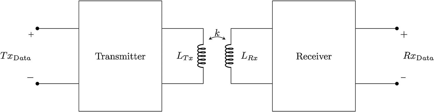
A transmitter and receiver circuit along with the on-chip inductors form a communication link, as depicted in Fig. 6.1. The transmitter, usually an H-bridge circuit, drives the inductor supplying a transmission current ![]() , while the receiver senses, amplifies, and rectifies the induced voltage
, while the receiver senses, amplifies, and rectifies the induced voltage ![]() into a digital pulse. A first order model of an inductive link is depicted in Fig. 6.2, illustrating the coupled on-chip inductors
into a digital pulse. A first order model of an inductive link is depicted in Fig. 6.2, illustrating the coupled on-chip inductors ![]() and
and ![]() . The parasitic resistance and capacitance of the on-chip spiral inductors are also depicted in this figure [259].
. The parasitic resistance and capacitance of the on-chip spiral inductors are also depicted in this figure [259].
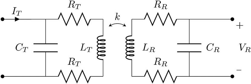
The inductively coupled link ideally behaves as a first order differentiator [260] ![]() , where
, where ![]() is the mutual inductance coupling between the transmitter and receiver inductors. However, due to the parasitic resistance and capacitance of the inductors, the link behaves as a band pass filter, with a peak at the resonance frequency
is the mutual inductance coupling between the transmitter and receiver inductors. However, due to the parasitic resistance and capacitance of the inductors, the link behaves as a band pass filter, with a peak at the resonance frequency ![]() , as determined by the self-inductance and parasitic capacitance of the inductors [261],
, as determined by the self-inductance and parasitic capacitance of the inductors [261],
(6.1)
The operation of the inductive link can be further explained by considering the link transfer function,
(6.2)
where the term 1/![]() (for
(for ![]() ) behaves as a second order low pass filter and constrains the bandwidth due to the losses of each inductor.
) behaves as a second order low pass filter and constrains the bandwidth due to the losses of each inductor.
Due to the short communication distance between the two inductors, pulse modulation is chosen as the communication scheme over carrier modulation. Pulse modulation is a simpler, low power communication scheme as opposed to carrier modulation, where complex analog and RF circuits are required. In the case of inductive links, the current ![]() of the transmitter produced by the digital pulse
of the transmitter produced by the digital pulse ![]() is modeled as a Gaussian pulse [261], as illustrated in Fig. 6.3A,
is modeled as a Gaussian pulse [261], as illustrated in Fig. 6.3A,
(6.3)
where ![]() and
and ![]() are, respectively, the magnitude and width of the pulse. Assuming an ideal inductive link, the voltage induced on the receiver
are, respectively, the magnitude and width of the pulse. Assuming an ideal inductive link, the voltage induced on the receiver ![]() , is the derivative of the transmitted pulse,
, is the derivative of the transmitted pulse,
(6.4)
as depicted in Fig. 6.3B. This voltage is described by a Gaussian double pulse given by [262a]
(6.5)

with an amplitude,
(6.5a)
The width ![]() of the current pulse is one of the primary parameters characterizing an inductive link. The sensitivity margin of the receiver is directly related to the width of the pulse, which is equal to
of the current pulse is one of the primary parameters characterizing an inductive link. The sensitivity margin of the receiver is directly related to the width of the pulse, which is equal to ![]() . Consequently, the pulse width also determines the operational bandwidth of the link. From the function describing the dependence on frequency of the induced voltage
. Consequently, the pulse width also determines the operational bandwidth of the link. From the function describing the dependence on frequency of the induced voltage ![]() , a peak frequency
, a peak frequency ![]() is observed. To avoid aliasing (or intersymbol interference), the operating frequency of the link should be greater than
is observed. To avoid aliasing (or intersymbol interference), the operating frequency of the link should be greater than ![]() . Therefore,
. Therefore,
(6.6)
provides a lower bound on the operating frequency of the communication scheme [261,262].
6.2 On-Chip Inductors for Intertier Links
The objective of an inductive link is to provide a high mutual inductance ![]() while maintaining the self-resonance frequency above the aliasing boundary,
while maintaining the self-resonance frequency above the aliasing boundary, ![]() . The design of the coil should therefore satisfy these two guidelines. The objective of a high mutual inductance or, in other words, intertier coupling, is explored in Section 6.2.1. Coil optimization with respect to link bandwidth specifications is discussed in Section 6.2.2.
. The design of the coil should therefore satisfy these two guidelines. The objective of a high mutual inductance or, in other words, intertier coupling, is explored in Section 6.2.1. Coil optimization with respect to link bandwidth specifications is discussed in Section 6.2.2.
6.2.1 Intertier Coupling Efficiency
Intertier coupling efficiency is intrinsically associated with the speed, power, and area of the inductive link. The overall quality of the link therefore greatly depends upon the coupling efficiency. A first order analysis of the coupling efficiency of inductive links is presented in this subsection.
Assuming an inductor with an outer diameter ![]() and a separation distance
and a separation distance ![]() , the coupling efficiency between the inductors is inversely proportional to X/
, the coupling efficiency between the inductors is inversely proportional to X/![]() [261]. Since the communication distance is usually limited by technology, the outer diameter of the coil is the primary parameter for adjusting the coupling efficiency. For a specific communication distance
[261]. Since the communication distance is usually limited by technology, the outer diameter of the coil is the primary parameter for adjusting the coupling efficiency. For a specific communication distance ![]() the coupling efficiency for decreasing the outer diameter of the coil is illustrated in Fig. 6.4.
the coupling efficiency for decreasing the outer diameter of the coil is illustrated in Fig. 6.4.

According to Fig. 6.4 the coupling efficiency can be divided into four discrete regions, the cubic, square, linear, and saturation regions. The difference among the regions depends upon the ratio X/![]() . For
. For ![]() ,
, ![]() is less than 0.1 and the coupling efficiency lies within the cubic region, which implies that the coupling efficiency is a cubic function of
is less than 0.1 and the coupling efficiency lies within the cubic region, which implies that the coupling efficiency is a cubic function of ![]() . In this region, the magnetic flux between the two inductors is severely attenuated. Communication can be achieved by utilizing multiple amplification stages at the receiver tier. Roughly the minimum
. In this region, the magnetic flux between the two inductors is severely attenuated. Communication can be achieved by utilizing multiple amplification stages at the receiver tier. Roughly the minimum ![]() for supporting low power intertier communication is
for supporting low power intertier communication is ![]() and is achieved at
and is achieved at ![]() , where the square region is approached.
, where the square region is approached.
The square region lies between ![]() to
to ![]() , or
, or ![]() . Synchronous receivers, in general, are used for communication when operating within the square region [261]. Synchronous circuits are preferred as these circuits exhibit lower bit error rates for low coupling as compared to asynchronous transceivers. Increasing the outer diameter allows the inductive link to enter the linear region, where asynchronous sensing schemes can be utilized. For diameter
. Synchronous receivers, in general, are used for communication when operating within the square region [261]. Synchronous circuits are preferred as these circuits exhibit lower bit error rates for low coupling as compared to asynchronous transceivers. Increasing the outer diameter allows the inductive link to enter the linear region, where asynchronous sensing schemes can be utilized. For diameter ![]() greater than
greater than ![]() the coupling efficiency saturates. The greater intertier coupling in the saturation region is usually exploited in wireless power transfer schemes, where increased efficiency is crucial. For data transmission schemes, the suggested coupling efficiency is
the coupling efficiency saturates. The greater intertier coupling in the saturation region is usually exploited in wireless power transfer schemes, where increased efficiency is crucial. For data transmission schemes, the suggested coupling efficiency is ![]() , or
, or ![]() . In Section 6.3, both synchronous and asynchronous inductive link receivers are considered where communication occurs within the different coupling regions.
. In Section 6.3, both synchronous and asynchronous inductive link receivers are considered where communication occurs within the different coupling regions.
6.2.2 Geometry and Electrical Characteristics of Inductor
The bandwidth of the link can be enhanced by proper design of the inductive link to achieve a specific coupling coefficient ![]() . Optimization of the coil is achieved by altering the geometry of the inductor. The electrical characteristics of the inductive link are also determined by the geometry of the inductor.
. Optimization of the coil is achieved by altering the geometry of the inductor. The electrical characteristics of the inductive link are also determined by the geometry of the inductor.
The geometry of the on-chip spiral inductor depends upon four parameters, the outer diameter ![]() , the number of turns
, the number of turns ![]() , the line width
, the line width ![]() , and the line spacing
, and the line spacing ![]() , as illustrated in Fig. 6.5. As mentioned in the previous subsection, the minimum outer diameter is limited by the communication distance to achieve a target coupling efficiency
, as illustrated in Fig. 6.5. As mentioned in the previous subsection, the minimum outer diameter is limited by the communication distance to achieve a target coupling efficiency ![]() . Consequently, the number of turns is chosen to manipulate the characteristics of the inductive link [259–262]. The line width and spacing are constrained by the fabrication process. Minimum line dimensions are usually employed, although a rule of thumb for the line width is 1% to 2% of
. Consequently, the number of turns is chosen to manipulate the characteristics of the inductive link [259–262]. The line width and spacing are constrained by the fabrication process. Minimum line dimensions are usually employed, although a rule of thumb for the line width is 1% to 2% of ![]() to reduce the parasitic resistance of the thin wires [261].
to reduce the parasitic resistance of the thin wires [261].

To quantify the effects of the inductor windings on the link characteristics, the complex relationship between the inductor geometry and the corresponding electrical parameters is explored here. The self-inductance of the spiral inductor structure is quadratically related to the number of turns,
(6.7)
Alternatively, the parasitic capacitance is linearly proportional to the number of turns
(6.8)
As a result, the self-resonance frequency is a function of ![]() ,
,
(6.9)
Consequently, changing the number of turns ![]() can adjust the link performance to satisfy the specifications of the communication scheme [261]. Based on the discussion in Section 6.2.1 and this subsection, the different aspects of the design process of the inductor are combined into a design flow that produces inductive links that satisfy specific performance, area, and power constraints.
can adjust the link performance to satisfy the specifications of the communication scheme [261]. Based on the discussion in Section 6.2.1 and this subsection, the different aspects of the design process of the inductor are combined into a design flow that produces inductive links that satisfy specific performance, area, and power constraints.
6.2.3 Design Flow for Inductive Link Coils
The design process of an inductive link scheme can require numerous iterations and be a time consuming process. A flow for designing the coils for an inductive link is illustrated in Fig. 6.6 and includes possible design iterations to satisfy power, performance, and/or area constraints.

To communicate across a distance ![]() the outer diameter
the outer diameter ![]() is chosen to satisfy a minimum coupling coefficient
is chosen to satisfy a minimum coupling coefficient ![]() . The outer diameter of the inductor is increased until the coupling coefficient
. The outer diameter of the inductor is increased until the coupling coefficient ![]() satisfies the minimum coupling constraint
satisfies the minimum coupling constraint ![]() . If this constraint is satisfied, the link bandwidth is improved by adjusting the inductor geometry; specifically, the number of spiral turns and trace width.
. If this constraint is satisfied, the link bandwidth is improved by adjusting the inductor geometry; specifically, the number of spiral turns and trace width.
The bandwidth of the inductive link is dependent on the communication scheme. Consequently, the bandwidth should satisfy the performance constraint of the link. Based on the coupling coefficient ![]() , minimum performance requirements, and area requirements, a synchronous or asynchronous scheme is chosen for the intertier signaling.
, minimum performance requirements, and area requirements, a synchronous or asynchronous scheme is chosen for the intertier signaling.
The transceiver circuit requires a specific output data rate, which is associated with the power consumption of the link. The link bandwidth can be refined to improve the link characteristics. The power consumption is the final design criterion to be assessed. Refinements to the design of the transceiver and the outer diameter of the inductor improve the power utilization of the link.
6.3 Transmitter and Receiver Circuits
Once the design of the coil is determined, the transmitter and receiver circuits that underpin the intertier communication are considered. Depending upon the coupling efficiency between the coils, a synchronous or asynchronous transceiver scheme can be utilized. The design of the synchronous inductive links is discussed in Section 6.3.1, while asynchronous sensing circuits are described in Section 6.3.2. High performance communication schemes with burst data transmission are reviewed in Section 6.3.3.
6.3.1 Design of Synchronous Inductive Link Transceivers
For low to moderate coupling efficiencies (![]() ), synchronous transceiver schemes are preferable. Synchronous receivers exhibit the advantage of noise immunity when sampling is off. As a result, noise is only induced when the received data are sampled. Consequently, the signal-to-noise ratio is improved and reliable communication is ensured.
), synchronous transceiver schemes are preferable. Synchronous receivers exhibit the advantage of noise immunity when sampling is off. As a result, noise is only induced when the received data are sampled. Consequently, the signal-to-noise ratio is improved and reliable communication is ensured.
A synchronous transceiver is schematically illustrated in Fig. 6.7 [261,262]. The transmitter is composed of an H-bridge circuit driving an inductor, augmented by a digital circuit for timing and signal shaping control. Alternatively, the receiver circuit comprises a sense amplifier for signal sensing and an SR latch to capture the received signal.
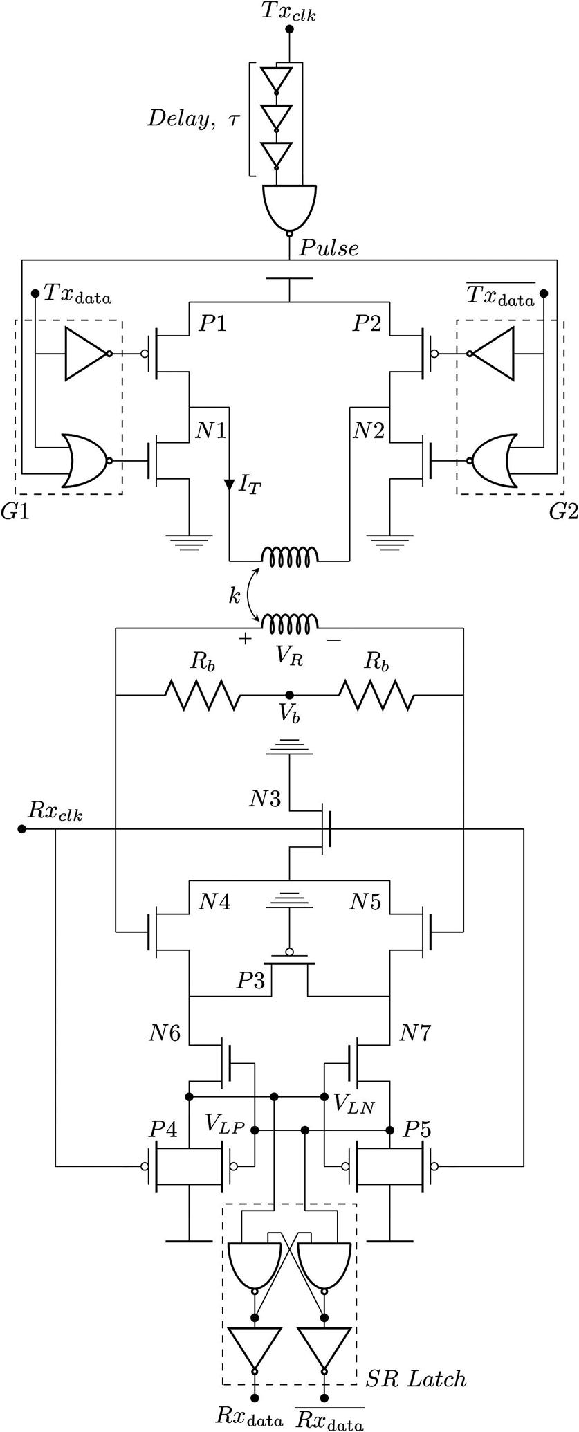
For the transmitter of the synchronous inductive link, a delay generator is used along with a clock signal to shape the pulse width, denoted by ![]() . The pulse width is the primary factor affecting the sensitivity of the receiver. For a pulse with width
. The pulse width is the primary factor affecting the sensitivity of the receiver. For a pulse with width ![]() , a positive edge in the transmitted data is sensed by transistors
, a positive edge in the transmitted data is sensed by transistors ![]() and
and ![]() (see Fig. 6.7), driven, respectively, by the inverter of block
(see Fig. 6.7), driven, respectively, by the inverter of block ![]() and the
and the ![]() gate of block
gate of block ![]() , producing a positive pulse. The amplitude of the generated pulse depends upon the size of the NMOS transistor
, producing a positive pulse. The amplitude of the generated pulse depends upon the size of the NMOS transistor ![]() . Likewise, a negative pulse is generated for a falling edge through transistors
. Likewise, a negative pulse is generated for a falling edge through transistors ![]() and
and ![]() .
.
Magnetic flux carries the generated pulses from the transmitter to the inductor at the receiver. The current generated at the receiver inductor is biased and amplified through the biasing resistance ![]() , with a resistance in the
, with a resistance in the ![]() range. The differential output of the resistance is passed to the sense amplifier through a differential amplifier stage. Two distinct operating stages of the sense amplifier exist, the precharge and evaluation stages. The amplifier alternates between those two stages depending upon the clock signal
range. The differential output of the resistance is passed to the sense amplifier through a differential amplifier stage. Two distinct operating stages of the sense amplifier exist, the precharge and evaluation stages. The amplifier alternates between those two stages depending upon the clock signal ![]() .
.
If the clock signal ![]() is low, the receiver circuit operates in the precharge phase, where transistors
is low, the receiver circuit operates in the precharge phase, where transistors ![]() and
and ![]() are switched on. The SR latch stores the data. Alternatively, if
are switched on. The SR latch stores the data. Alternatively, if ![]() is high, the PMOS transistors are off. Depending upon the polarity of
is high, the PMOS transistors are off. Depending upon the polarity of ![]() and
and ![]() , respectively, the voltage at either node
, respectively, the voltage at either node ![]() or node
or node ![]() is pulled to logic high, driving the other input to a logic low. Thus, the polarity of the transmitted data
is pulled to logic high, driving the other input to a logic low. Thus, the polarity of the transmitted data ![]() is replicated. In the following precharge phase, the SR latch maintains the polarity of the pulse and generates the digital signal
is replicated. In the following precharge phase, the SR latch maintains the polarity of the pulse and generates the digital signal ![]() .
.
6.3.2 Asynchronous Data Transmission and Recovery
When operating in the linear region, asynchronous data transceivers for communication are typically used. The size of the transceiver circuit is much smaller since the timing control blocks are less complex. The effect is increased communication speed of the inductive link since the data rate of the channel is not limited by the timing circuit. Alternatively, the interface bottleneck is either the switching frequency of the transistors or the bandwidth supported by the pair of inductors (whichever is lower).
The asynchronous transceiver, shown in Fig. 6.8 [264], features an H-bridge circuit driving the inductor, similar to the equivalent synchronous circuit. Nevertheless, the timing circuit is removed, reducing overall area and yielding higher performance in terms of both communication speed and power. The timing circuit is also removed from the receiver circuit, where a hysteresis comparator is used rather than a sense amplifier.
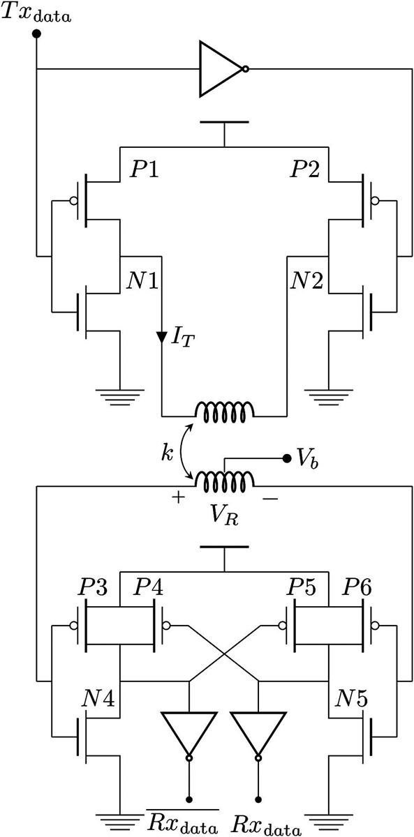
In the receiving tier, a hysteresis comparator senses the induced data. The hysteresis comparator includes a gain stage (devices ![]() and
and ![]() ) and a latch circuit (see Fig. 6.8). The induced voltage
) and a latch circuit (see Fig. 6.8). The induced voltage ![]() is biased at voltage
is biased at voltage ![]() and is inputted differentially to the hysteresis comparator. Depending upon the polarity of the induced signal, the hysteresis comparator is driven to either an on or off state, reproducing the transmitted data signal without requiring a clock signal. The sensitivity of the receiver circuit depends upon the change in hysteresis voltage
and is inputted differentially to the hysteresis comparator. Depending upon the polarity of the induced signal, the hysteresis comparator is driven to either an on or off state, reproducing the transmitted data signal without requiring a clock signal. The sensitivity of the receiver circuit depends upon the change in hysteresis voltage ![]() of the comparator. The change in the hysteresis voltage has the opposite polarity as compared to the output signal
of the comparator. The change in the hysteresis voltage has the opposite polarity as compared to the output signal ![]() , and is modulated by a latch circuit. For a positively induced pulse, the signal
, and is modulated by a latch circuit. For a positively induced pulse, the signal ![]() transitions high and the latch circuit reduces the voltage threshold of the comparator by the change in the hysteresis voltage,
transitions high and the latch circuit reduces the voltage threshold of the comparator by the change in the hysteresis voltage, ![]() , where
, where ![]() is the threshold voltage of the comparator and
is the threshold voltage of the comparator and ![]() , the threshold voltage of the gain devices. The threshold voltage of the comparator facilitates the transition for the following negative pulse. The output signal is therefore held high until a negative edge is received. Similarly, an equivalent procedure is followed for a negative pulse.
, the threshold voltage of the gain devices. The threshold voltage of the comparator facilitates the transition for the following negative pulse. The output signal is therefore held high until a negative edge is received. Similarly, an equivalent procedure is followed for a negative pulse.
As mentioned previously, an asynchronous communication scheme requires increased coupling efficiency to cope with signal reliability. Increased coupling efficiency can be achieved with larger inductors, which, however, lead to increased area for the inductive link. To mitigate the greater area, multiplexing techniques are applied, such as burst data transmission [264].
6.3.3 Burst Data Transmission
Due to the size of the inductors in the inductive link, only a few links can fit within a circuit without requiring excessive area. Increasing the number of on-chip inductors can lead to area consuming or, in many cases, overly congested circuits, since the inductors are placed within the global interconnect layers. An efficient method is needed to exploit the available bandwidth of the inductive link without further increasing area. Consequently, data multiplexing schemes, such as the approach illustrated in Fig. 6.9, are utilized to reduce the number of inductive links.

Data multiplexing provides several advantages when applied to inductive links. The number of individual inductive links decreases, reducing proportionally the area requirements. Moreover, fewer transmitter circuits dissipate less power. Depending upon the circuit, an inductive link transmitter can demand high power. An array of transmitters can consume significant power as compared to a single inductive link transmitter combined with a multiplexing scheme. Thus, less power is consumed if burst transmission is employed.
The performance of the burst transmission scheme depends upon the clock frequency of the multiplexer and demultiplexer as the clock signal is the primary bandwidth bottleneck of the circuit. To achieve a high frequency, a low power clock generator, such as a ring oscillator circuit with a counter, is often preferred to control the length of the transmission. An inductive link with burst transmission for mobile devices is described in [264], where a 400 MHz clock is assumed for the processor. As a result, a ![]() clock is generated by a local ring oscillator for multiplexing and demultiplexing eight signals. To avoid the use of a second ring oscillator on the receiving tier, the clock signal is transmitted over an inductive link.
clock is generated by a local ring oscillator for multiplexing and demultiplexing eight signals. To avoid the use of a second ring oscillator on the receiving tier, the clock signal is transmitted over an inductive link.
6.4 Challenges for Wireless On-Chip Communication
Wireless intertier communication provides plenty of advantages for 3-D integration, particularly for heterogeneous circuits. Nevertheless, challenges arise that can hinder the use of wireless interfaces for on-chip communication. Wireless systems are based on passive inductors and capacitors, which consume significant area as compared to active devices. Area optimization is therefore an important issue in the design of inductive links. Moreover, wireless interfaces suffer from coupling noise that should be considered during the design process. Coupling noise is crosstalk between inductive links due to the close proximity or noise induced by the inductive link on other vital and noise sensitive on-chip components, such as the power delivery network. Moreover, the lack of a wired interconnect interface introduces challenges to delivering power to all of the tiers except for the tier connected to the package substrate. A performance and area analysis of the inductive links is described in Section 6.4.1. Crosstalk issues between inductive links are explored in Section 6.4.2, while crosstalk noise effects caused by the inductive link on the power delivery system are discussed in Section 6.4.3.
6.4.1 Performance and Area Analysis
Recent works on TSV signaling and bandwidth optimization indicate that TSVs can achieve high data rates [265,266]. Inductive links are also capable of achieving performance levels comparable to TSVs [257]. The area requirements between the two communication schemes, nevertheless, are considerably different. TSVs occupy both silicon and wiring area, while inductive links primarily require interconnect resources. To model this situation, a performance-to-area metric is introduced to provide a fair comparison [257],
(6.10)
where ![]() is the communication bandwidth achieved by each interface and
is the communication bandwidth achieved by each interface and ![]() is the area.
is the area.
To evaluate performance, an ![]() model of the TSV is utilized which includes parasitic capacitive coupling with the substrate and other neighboring TSVs. Different state-of-the-art TSV pitches are considered to model the effect of coupling on TSV performance. Moreover, the redistribution layer of the TSV is also considered in the model, since this layer adds parasitic resistance and capacitance and dominates the delay of the intertier interfaces. These models are frequency dependent, since communication in a high performance system is assumed. The behavior of the model changes significantly at high frequencies.
model of the TSV is utilized which includes parasitic capacitive coupling with the substrate and other neighboring TSVs. Different state-of-the-art TSV pitches are considered to model the effect of coupling on TSV performance. Moreover, the redistribution layer of the TSV is also considered in the model, since this layer adds parasitic resistance and capacitance and dominates the delay of the intertier interfaces. These models are frequency dependent, since communication in a high performance system is assumed. The behavior of the model changes significantly at high frequencies.
An asynchronous inductive link transceiver is evaluated based on a state-of-the-art on-chip inductor [264]. The performance of the inductive link is evaluated with SPICE, achieving a maximum data rate of 20 Gbps. The inductors considered in this analysis are chosen to ensure that the communication distance supported by the inductive link is comparable to the length of the TSVs. Both inductive links and TSVs are placed in an ![]() array to form a high performance communication interface.
array to form a high performance communication interface.
The bandwidth-area efficiency for each interface is listed in Table 6.1. To determine the interconnect efficiency, a six metal layer interconnect technology is assumed. The silicon area efficiency ![]() , interconnect area efficiency
, interconnect area efficiency ![]() , and total efficiency
, and total efficiency ![]() are reported for each type of interface
are reported for each type of interface ![]() (i.e., TSV or IL). As the TSV pitch increases, the overall efficiency drops by
(i.e., TSV or IL). As the TSV pitch increases, the overall efficiency drops by ![]() . The TSV link efficiency, however, remains almost five times greater than the efficiency of an inductive link. The efficiency of the interconnect layers follows the overall efficiency, with the TSV interface presenting a significantly higher performance-to-area ratio.
. The TSV link efficiency, however, remains almost five times greater than the efficiency of an inductive link. The efficiency of the interconnect layers follows the overall efficiency, with the TSV interface presenting a significantly higher performance-to-area ratio.
Table 6.1
Performance-to-Area Efficiency for Single Interface Links
| Type of Interface | |||
| TSV, 20 μm | 71.2 | 11.8 | 71.2 |
| TSV, 30 μm | 21.7 | 3.6 | 21.7 |
| TSV, 40 μm | 13.8 | 2.3 | 13.8 |
| IL, 84 μm | 2.7×10³ | 1.4 | 2.8 |

The silicon area efficiency, however, leads to a different result. Since the transceiver used by the inductive link is a small circuit, the silicon area efficiency of the inductive link is an order of magnitude greater than the efficiency of a TSV. The silicon area underneath the on-chip inductor can be used to either reduce the area overhead of the interface, or improve the performance-to-area efficiency of the inductive interface.
A multiplexing scheme can improve the performance of the inductive interface by reducing the number of on-chip inductors. The same multiplexing scheme is compared with the TSV interface. For simplicity, a 1 Gbps data rate is assumed for a communication channel. Multiplexing decreases the area of a TSV link, although multiplexing limits the data rate due to the latency imposed by the multiplexing–demultiplexing circuitry. Depending upon the diameter of the TSV and the size of the multiplexer, the area efficiency of the TSV interface departs from the aforementioned bounds. For an inductive link, however, considerable silicon area is available. This area can be reserved for multiplexing without incurring any additional area as compared to a TSV link. A tradeoff between the multiplexing ratio and the performance-to-area efficiency of the interfaces exists to determine the highest area efficiency to achieve a specific performance.
A multiplexing ratio of up to 12:1 is used by the multiplexer described in [267]. The interface efficiency is depicted in Fig. 6.10 for each scheme. For the TSV interface, two trends can be observed. For a TSV pitch smaller than ![]() , the interface performs better without multiplexing. As the multiplexing ratio increases, the efficiency drops. However, for a TSV with a pitch greater than
, the interface performs better without multiplexing. As the multiplexing ratio increases, the efficiency drops. However, for a TSV with a pitch greater than ![]() , multiplexing increases system efficiency. As shown in Fig. 6.10,
, multiplexing increases system efficiency. As shown in Fig. 6.10, ![]() asymptotically approaches 1.5 Mbps/μm2.
asymptotically approaches 1.5 Mbps/μm2.
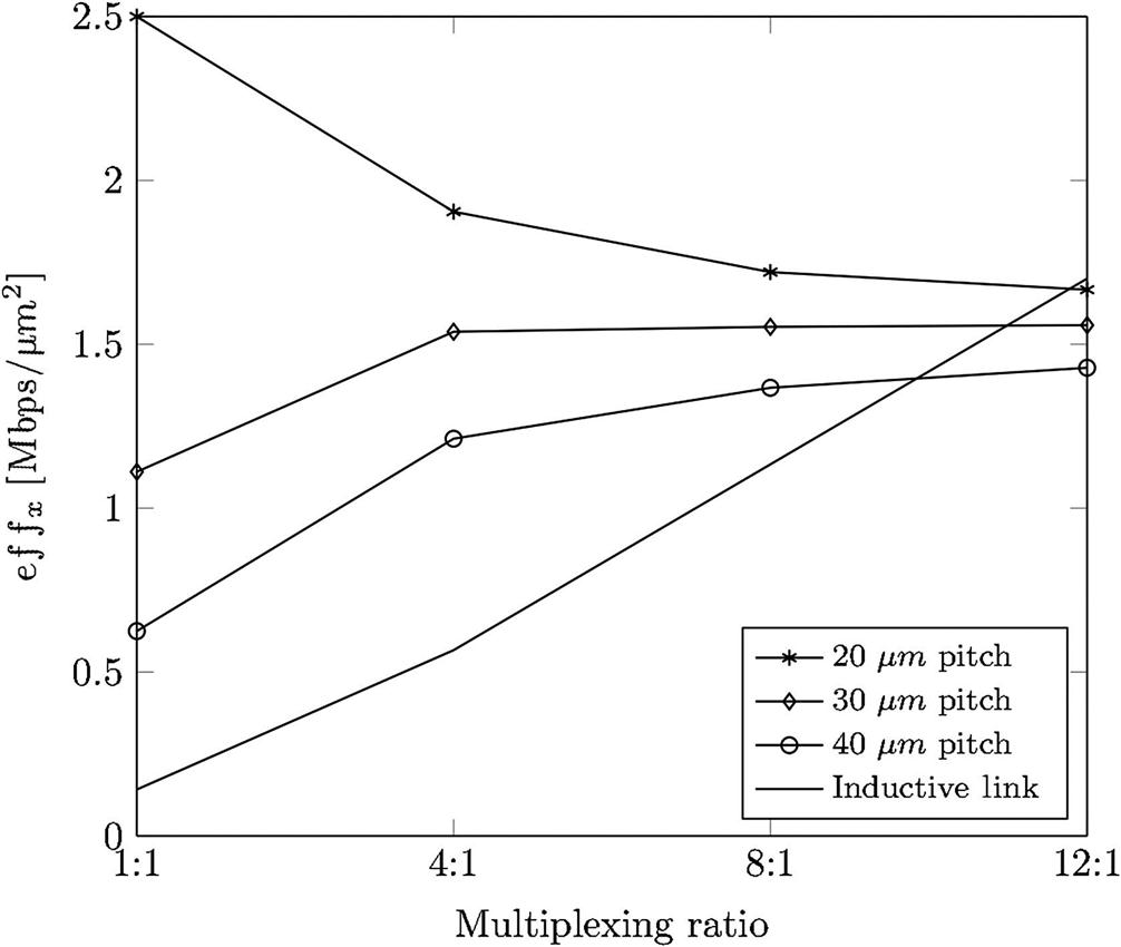
This behavior occurs since the multiplexing circuits require greater area as compared to the TSVs. For a data rate of 1 Gbps and no multiplexing, the size of the interface circuit is similar to the area occupied by the TSVs. A decreasing TSV diameter leads to a quadratic increase in the area efficiency of the interface. However, if signal multiplexing is included, this behavior changes. As the multiplexing ratio increases, the efficiency of the interface saturates to a level depending upon the ratio of the pitch of the TSV to the area of the multiplexer.
The performance-to-area density for each communication scheme exhibits comparable performance, while the area significantly differs. Combined with a high density multiplexing scheme, an inductive link can exhibit comparable or even improved performance density as compared to a state-of-the-art TSV interface. Nevertheless, TSVs with a sub-20 μm pitch provide the best efficiency without signal multiplexing.
6.4.2 Crosstalk Between Inductive Links
Inductive links control magnetic flux and employ pulse modulation for near communication between different tiers within a 3-D system. Unavoidably, crosstalk noise exists between different inductive links when placed in high density arrays in high performance interconnect interfaces. A method based on time division multiplexing can be used to mitigate crosstalk between inductive links, as discussed in this subsection.
Electromagnetic coupling between inductive links occurs due to the high density required for increased performance and area efficiency. A straightforward method to reduce interlink noise is to increase the distance between neighboring inductors. For a space of ![]() , where
, where ![]() is the outer diameter of the inductor, the induced noise is negligible and the nearby channels do not affect the inductive link [268]. However, doubling the distance between links effectively quadruples the area required by the communication interface. An area efficient solution is, therefore, needed to improve the performance of a link while reducing crosstalk noise.
is the outer diameter of the inductor, the induced noise is negligible and the nearby channels do not affect the inductive link [268]. However, doubling the distance between links effectively quadruples the area required by the communication interface. An area efficient solution is, therefore, needed to improve the performance of a link while reducing crosstalk noise.
An effective way to reduce crosstalk between inductive links is to avoid simultaneous operation of adjacent links. An example of this approach is time division interleaving, as described in [268] for an 1 Tbps inductive coupling transceiver. A four-phase clock is generated by a phase interpolator, dividing the operation of a block of transceivers into several time slots. To achieve a data rate of 1 Gbps/link, a 1 GHz clock is applied and each inductive link occupies an operating time slot of 250 ps per clock cycle. 1,024 transceivers operate in parallel to achieve the 1 Tbps performance objective.
These results indicate that without the time interleaving technique, the crosstalk noise induced in adjacent links is similar to the voltage amplitude of the received signal (50 mV). The bit error rate of the channel in this case is significantly higher. However, for a two-phase interleaving scheme, the induced crosstalk noise is reduced to half (25 mV), improving the performance of the communication channel. A four-phase time division solution further improves performance, where an amplitude of 10 mV is observed for the crosstalk noise.
6.4.3 Crosstalk Noise on Adjacent On-Chip Components
A byproduct of contactless on-chip communication is interference with other components within a system due to the wireless nature of the scheme. For example, adjacent interconnect layers, analog circuits, or sensitive digital circuits may be affected by electromagnetic waves emitted from an inductive link. Alternatively, interconnects could also affect the behavior of the inductor. Interactions between the inductor and interconnect layers, as well as noise induced by the inductive link and mitigation techniques to dampen this noise, are described in this subsection. The crosstalk produced by a single inductor link is discussed in Section 6.4.3.1. The more complex case of crosstalk due to an array of inductive links is described in Section 6.4.3.3. The resulting noise due to the crosstalk on diverse power distribution topologies is evaluated in Section 6.4.3.4.
6.4.3.1 Crosstalk effects due to an inductive link
The effect on the performance of an inductive link due to the interconnect wires in the vicinity of the spiral inductors is explored in [269]. Different types of power lines have been evaluated to model the effect of inductive links. Experimental results demonstrate that interconnects that form a closed loop are susceptible to eddy currents, reducing the performance of inductive links. Denser interconnect topologies, such as a mesh grid, exhibit higher transimpedance losses within an inductor, requiring greater transmission power to achieve the same performance.
Conversely, the effect of an inductive link on sensitive digital circuits has also been considered. An SRAM module is assumed with a sensing voltage of 50 mV. Placing an inductive link in the vicinity of an SRAM module induces a coupling noise pulse of 1 mV. The effect of the inductive link is therefore negligible as compared to the sensing voltage of the SRAM, and no read errors are induced due to the inductive link. Consequently, inductive links can be used in combination with SRAM in high density applications, such as a memory interface for a processor.
Since the on-chip inductors are placed on the topmost interconnect layers, crosstalk can, however, occur between the inductive link and a nearby power delivery network [270]. The induced noise from the inductive link adds to the other noise components of the power delivery network such as ![]() drops due to the wire resistance and simultaneous switching noise (SSN)
drops due to the wire resistance and simultaneous switching noise (SSN) ![]() caused by device switching.
caused by device switching.
Each closed path formed within a power delivery network is susceptible to eddy currents and, consequently, voltage fluctuations induced by the inductor. Closed paths are formed between two or more power or ground wires. The amplitude of the induced voltage on the power delivery network depends upon the geometric and electrical characteristics of the return path, altering the coupling between the inductor and the power delivery network. Furthermore, the induced voltage depends upon the magnetic flux density that changes according to the spatial position of the power delivery network with respect to the inductor.
Standard design methods and CAD tools for power distribution networks consider ![]() drop and
drop and ![]() noise [271]. Traditional design processes for power delivery networks, however, do not consider the additional noise originating from the interchip inductors in contactless 3-D systems. To address the combined effects of noise for power delivery networks, including SSN and resistive
noise [271]. Traditional design processes for power delivery networks, however, do not consider the additional noise originating from the interchip inductors in contactless 3-D systems. To address the combined effects of noise for power delivery networks, including SSN and resistive ![]() drops, the spatial alignment of the power and ground (P/G) loops with respect to the inductive link should be considered during the design process. Crosstalk coupling between the inductors and the P/G wires can lead to high levels of power noise. Measures are necessary to remedy this situation.
drops, the spatial alignment of the power and ground (P/G) loops with respect to the inductive link should be considered during the design process. Crosstalk coupling between the inductors and the P/G wires can lead to high levels of power noise. Measures are necessary to remedy this situation.
6.4.3.2 Case study
A structure consisting of an inductive link and a return path through a power delivery network has been evaluated with Ansys high frequency structural simulator (HFSS) to quantify the noise induced by an inductive link [272]. The simulated structure is illustrated in Fig. 6.11. A flip chip face-to-back integration approach is assumed. The length of the interconnect is denoted as ![]() . Distance
. Distance ![]() denotes the spatial separation between the geometric center of the inductor
denotes the spatial separation between the geometric center of the inductor ![]() and the geometric center of the return path through the interconnect loop. A power loop is assumed; however, the same investigation also applies to the ground loop.
and the geometric center of the return path through the interconnect loop. A power loop is assumed; however, the same investigation also applies to the ground loop.
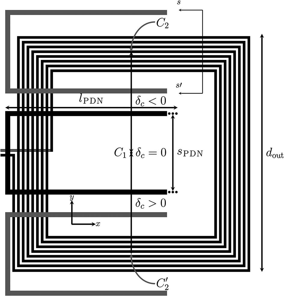
The noise amplitude varies considerably with the relative location of the interconnect with respect to the center of the inductors due to the different level of magnetic flux flowing through the power loop. To model this behavior, parameter ![]() is used to notate the relative location between the power loop and the inductors, where
is used to notate the relative location between the power loop and the inductors, where ![]() is swept within the range
is swept within the range ![]() . Three positions with respect to the inductor,
. Three positions with respect to the inductor, ![]() ,
, ![]() , and
, and ![]() , are shown in Fig. 6.11, where, respectively,
, are shown in Fig. 6.11, where, respectively, ![]() ,
, ![]() , and
, and ![]() . For
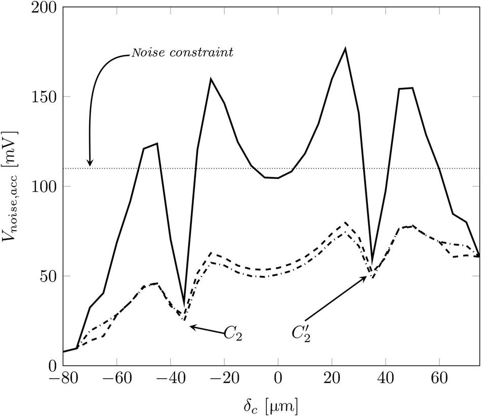
. For ![]() , the amplitude of the noise is negligible, as shown in Fig. 6.12 by the crosshatched area. A maximum induced noise
, the amplitude of the noise is negligible, as shown in Fig. 6.12 by the crosshatched area. A maximum induced noise ![]() of 39.5 mV is observed, where the power loop is close to the windings of the inductor. Alternatively, a considerable dip in the induced noise is observed for
of 39.5 mV is observed, where the power loop is close to the windings of the inductor. Alternatively, a considerable dip in the induced noise is observed for ![]() , decreasing to
, decreasing to ![]() of 4.6 mV.
of 4.6 mV.

This outcome is due to the opposite direction of the magnetic flux between the two wires of the power loop, where the power loop is placed at either ![]() or
or ![]() , as shown in Fig. 6.11. This behavior indicates that there is no need to place the power loop far from the inductive link to avoid crosstalk. Instead, due to the opposite direction of coupling between the wires of the loop and the turns of the inductor, the crosstalk is low without greatly altering the power delivery network.
, as shown in Fig. 6.11. This behavior indicates that there is no need to place the power loop far from the inductive link to avoid crosstalk. Instead, due to the opposite direction of coupling between the wires of the loop and the turns of the inductor, the crosstalk is low without greatly altering the power delivery network.
6.4.3.3 Crosstalk noise effects caused by inductive link arrays
Inductive links are typically placed in a high density array to increase the communication performance of the interface. To estimate the noise in this case, an array of ![]() inductive links is assumed with a spacing of 30 μm between each link to reduce crosstalk during simultaneous transmission. Each inductive link consists of transceiver and multiplexing circuits, consuming a current of I=7.1 mA, modeled as uniformly distributed current sources across each inductor. The array is supplied by a power grid that utilizes the global and intermediate metal layers of a 65 nm process node. The grid produces an
inductive links is assumed with a spacing of 30 μm between each link to reduce crosstalk during simultaneous transmission. Each inductive link consists of transceiver and multiplexing circuits, consuming a current of I=7.1 mA, modeled as uniformly distributed current sources across each inductor. The array is supplied by a power grid that utilizes the global and intermediate metal layers of a 65 nm process node. The grid produces an ![]() drop of 13.8 mV, which satisfies typical power supply noise constraints (<5% to 10% of Vdd). The power loops on the topmost global layer are illustrated in Fig. 6.13 as solid lines. The power loops span the entire array connecting to C4 bumps placed symmetrically at the periphery of the array. A spacing of
drop of 13.8 mV, which satisfies typical power supply noise constraints (<5% to 10% of Vdd). The power loops on the topmost global layer are illustrated in Fig. 6.13 as solid lines. The power loops span the entire array connecting to C4 bumps placed symmetrically at the periphery of the array. A spacing of ![]() and a diameter of
and a diameter of ![]() are assumed for the bumps, satisfying the minimum area requirements for C4 pads [273]. The surrounding C4 bumps are assumed to supply the total current drawn by the array of inductors at a nominal
are assumed for the bumps, satisfying the minimum area requirements for C4 pads [273]. The surrounding C4 bumps are assumed to supply the total current drawn by the array of inductors at a nominal ![]() of 1.1 V. The bumps are connected to the power and ground lines through, respectively, the resistances
of 1.1 V. The bumps are connected to the power and ground lines through, respectively, the resistances ![]() and
and ![]() .
.

The accumulated noise from a row within the inductive link array is illustrated in Fig. 6.14. The dashed line denotes the noise of an inductor at the edge of the array while the dash dotted line is the noise of an inductor at the middle of the line. The ![]() drop is superimposed on both curves. The solid line is the total noise for a row within the inductor array, based on
drop is superimposed on both curves. The solid line is the total noise for a row within the inductor array, based on
(6.11)
where ![]() is the noise generated from the inductors placed at the edge of the loop.
is the noise generated from the inductors placed at the edge of the loop. ![]() is the noise produced by the remaining
is the noise produced by the remaining ![]() inductors coupled to the power delivery network loop, where
inductors coupled to the power delivery network loop, where ![]() for the example illustrated in Fig. 6.13. Spatial alignment of the power grid over certain positions, such as
for the example illustrated in Fig. 6.13. Spatial alignment of the power grid over certain positions, such as ![]() and
and ![]() depicted in Fig. 6.11, results in minimum noise caused by the inductor. The corresponding positions to produce minimum noise for the structure shown in Fig. 6.13 are also shown in Fig. 6.14 for different
depicted in Fig. 6.11, results in minimum noise caused by the inductor. The corresponding positions to produce minimum noise for the structure shown in Fig. 6.13 are also shown in Fig. 6.14 for different ![]() .
.
Considering the first row of the inductive links, as shown in Fig. 6.13, the power loop is placed at position ![]() , yielding a total noise
, yielding a total noise ![]() of 35.4 mV. Moreover, the ground loop can be placed at
of 35.4 mV. Moreover, the ground loop can be placed at ![]() , where the accumulated noise
, where the accumulated noise ![]() is 59.1 mV. The noise is slightly higher as compared to the power loop due to the increased
is 59.1 mV. The noise is slightly higher as compared to the power loop due to the increased ![]() drop. The overall power noise is less than 8.2%. The initial placement of the power grid exhibits low
drop. The overall power noise is less than 8.2%. The initial placement of the power grid exhibits low ![]() drop. The induced noise can however violate the allowed power noise constraint, reaching
drop. The induced noise can however violate the allowed power noise constraint, reaching ![]() of 320 mV if the worst case position for both the power and ground loops is assumed. Proper placement of the power grid is therefore required to satisfy a low noise constraint despite interference from the inductive links.
of 320 mV if the worst case position for both the power and ground loops is assumed. Proper placement of the power grid is therefore required to satisfy a low noise constraint despite interference from the inductive links.
6.4.3.4 Noise sensitivity of power network topologies
A similar analysis can be applied to determine the sensitivity to noise for other power delivery topologies, which depends upon the geometric characteristics of these networks. The sensitivity to induced noise is described in [274] for different power delivery network topologies, assuming an interdigitated power delivery network with either a paired type-I or a paired type-II topology [185,275,276]. Several power delivery network topologies are depicted in Fig. 6.15.
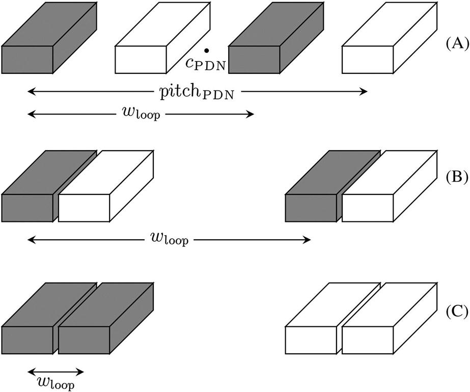
The center and pitch of an elemental power delivery network segment, denoted, respectively, as ![]() and
and ![]() , are also shown in Fig. 6.15. As the width of the loop
, are also shown in Fig. 6.15. As the width of the loop ![]() between the power or ground wires is different for each topology,
between the power or ground wires is different for each topology, ![]() is used for all of the topologies to provide a fair comparison. The center of the power delivery network segment
is used for all of the topologies to provide a fair comparison. The center of the power delivery network segment ![]() describes the relative spatial position of the power delivery network with respect to an inductive link. The same inductive link structure is considered, as shown in Fig. 6.13, to evaluate the accumulated noise produced by an inductive link.
describes the relative spatial position of the power delivery network with respect to an inductive link. The same inductive link structure is considered, as shown in Fig. 6.13, to evaluate the accumulated noise produced by an inductive link.
An analysis of a ![]() array of inductive links is reported in [274]. Several cases are listed in Table 6.2 for each power delivery network topology for pairs of
array of inductive links is reported in [274]. Several cases are listed in Table 6.2 for each power delivery network topology for pairs of ![]() that satisfy a 10% noise constraint. The induced noise
that satisfy a 10% noise constraint. The induced noise ![]() described by (6–11) is also provided, which considers the induced noise on both the power and ground loops.
described by (6–11) is also provided, which considers the induced noise on both the power and ground loops.
Table 6.2
Accumulated Noise for Different Power Delivery Network Geometries
| Topology | Geometry | Total |
Overall Noise | ||||
| Power Loop | Ground Loop | ||||||
| Interdigitated | 45 | −45 | 108 | 5.25 | 18.1 | 131.3 | 13.9% (fail) |
| 45 | 70 | 92 | 52.8 | 61.3 | 153.8 | 18.1% (fail) | |
| Paired Type-I | 45 | −40 | 56.1 | 11.1 | 14.1 | 81.3 | 7.3% (pass) |
| 60 | −40 | 59.2 | 14.2 | 6.1 | 79.5 | 7.2% (pass) | |
| 105 | −50 | 69.2 | 35.2 | 27.7 | 132.1 | 12% (fail) | |
| 105 | 50 | 69.2 | 56.2 | 63.7 | 189.1 | 17.1% (fail) | |
| Paired Type-II | 45 | −35 | 58.1 | 9.7 | 27.2 | 95 | 8.6% (pass) |
| 75 | −45 | 65.3 | 16.7 | 26.3 | 108.3 | 9.8% (pass) | |
| 90 | 0 | 28.5 | 10.8 | 45.5 | 84.8 | 7.7% (pass) | |
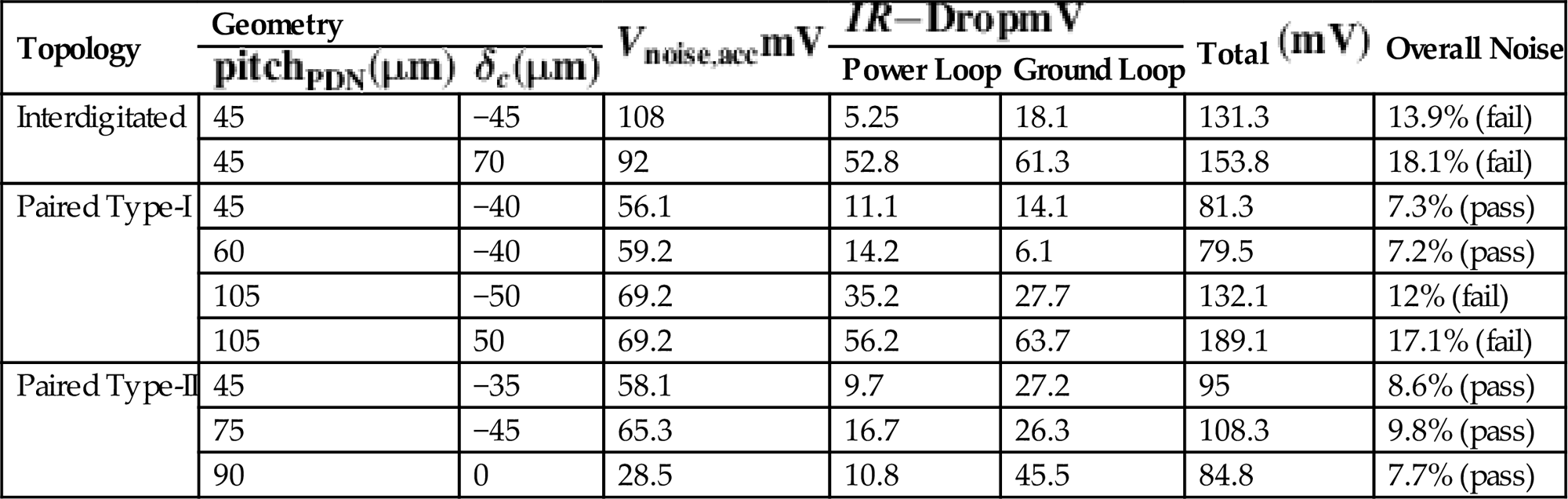
The interdigitated topology exhibits a higher sensitivity to induced noise as compared to the paired topologies. Even in the location where the induced noise is minimum, the added ![]() drop for the power and ground loops increases the total noise to prohibitive levels. Overall, a minimum noise of
drop for the power and ground loops increases the total noise to prohibitive levels. Overall, a minimum noise of ![]()
![]() is noted, surpassing the
is noted, surpassing the ![]() noise constraint.
noise constraint.
Alternatively, both paired topologies include a ![]() configuration where the overall noise is below the target limit. For the type-I topology, a noise level of
configuration where the overall noise is below the target limit. For the type-I topology, a noise level of ![]() is achieved, well below the target limit. The overall noise primarily occurs due to the induced noise, while the added
is achieved, well below the target limit. The overall noise primarily occurs due to the induced noise, while the added ![]() drop is relatively small for valid spatial positions. For the type-II topology, the ground loop
drop is relatively small for valid spatial positions. For the type-II topology, the ground loop ![]() drop significantly increases the overall noise due to the greater distance from the pads. Nevertheless, positions exist where the overall noise level is tolerable, such as the positions shown in Fig. 6.13, exhibiting an overall noise of
drop significantly increases the overall noise due to the greater distance from the pads. Nevertheless, positions exist where the overall noise level is tolerable, such as the positions shown in Fig. 6.13, exhibiting an overall noise of ![]() (listed in Table 6.2).
(listed in Table 6.2).
6.5 Intertier Power Transfer
Inductive links enable intertier communication without the need for expensive TSVs or microbumps. Moreover, through silicon communication can be supported within multiple tiers due to the low attenuation of the magnetic flux passing through the resistive substrate, in comparison, for example, to the attenuation of the electric field in capacitive links [258]. Consequently, face-up and back-to-back bonding styles can also be exploited as well as face-to-face integration. The challenge of delivering power to the upper tiers without a wired solution potentially increases cost and manufacturing complexity. Wireless power transfer is discussed in this section as a means to overcome this problem.
Similar to inductive data links, a transmitter inductor generates magnetic flux that couples to the powered tiers through the inductor at the receiver. The received magnetic flux induces a current in the receiver inductor that is rectified and regulated to behave as a DC power source, as illustrated in Fig. 6.16. On-chip wireless power transfer is achieved in several ways. Standard inductive coupling and resonant inductive coupling are examples of wireless power delivery schemes [277].
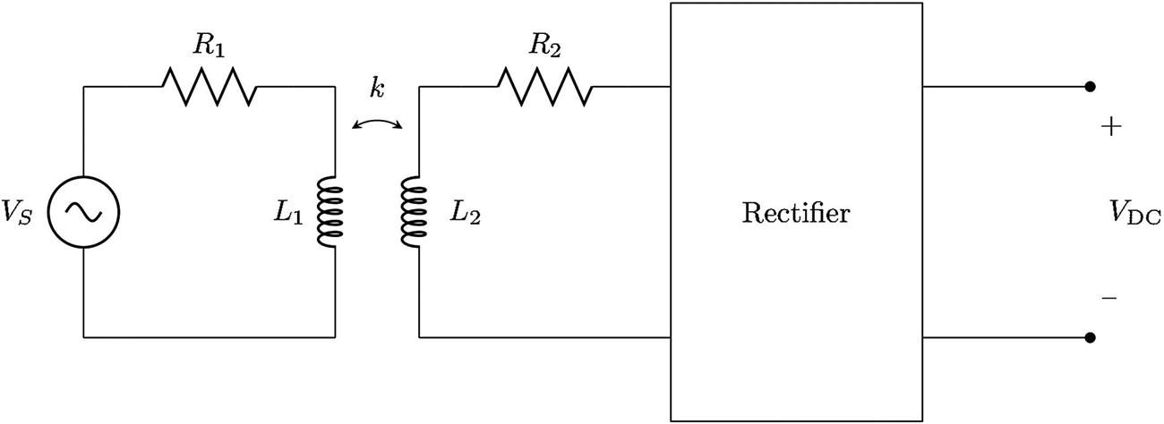
With standard inductive coupling, the parasitic impedance of the inductors, primarily the parasitic impedance of the transmitter inductor, affects the performance of the interface circuitry. The quality factor ![]() of the inductor must be increased to enhance power transmission, where
of the inductor must be increased to enhance power transmission, where ![]() is the parasitic resistance of the inductors. A low parasitic resistance
is the parasitic resistance of the inductors. A low parasitic resistance ![]() is therefore a primary issue in wireless power delivery. With a lower resistance, higher currents can flow through the high
is therefore a primary issue in wireless power delivery. With a lower resistance, higher currents can flow through the high ![]() inductor, providing greater power efficiency or support longer signal transmission distances. The operating frequency of the inductive interface is determined by the characteristics of the integrated inductors. The interface operates as a band pass filter and, therefore, appropriate selection of the operating frequency will enhance the power efficiency. Note that the transmitter and receiver inductors can exhibit different physical and electrical characteristics.
inductor, providing greater power efficiency or support longer signal transmission distances. The operating frequency of the inductive interface is determined by the characteristics of the integrated inductors. The interface operates as a band pass filter and, therefore, appropriate selection of the operating frequency will enhance the power efficiency. Note that the transmitter and receiver inductors can exhibit different physical and electrical characteristics.
A wireless power transmission interface for 3-D integrated systems is described in [278]. A power transmission of 2.5 mW is achieved for a face-to-face 3-D configuration with a communication distance below 20 μm. A ring oscillator drives the transmitter inductor, while cross-coupled PMOS diodes rectify the voltage at the receiver side. A resistive load of 100 Ω is connected to the rectifier, matching the source resistance, thereby maximizing the power transfer efficiency.
Another contactless power delivery system with improved efficiency is reported in [279]. An H-bridge circuit drives the transmitter inductor on the top tier. The substrate of the top tier is thinned to maintain operation of the link under different communication distances, specifically 15, 50, and 250 μm. Alternatively, the receiver consists of a sensing inductor and four cross-coupled diodes which function as a rectifier and a resistive load. The transceiver operates as a band pass filter with a center frequency of 140 MHz.
The power delivery efficiency depends upon the distance between the coupled inductors and the operating frequency of the transceiver. The efficiency of the power delivery scheme is dependent on the parasitic resistance and capacitance of the inductors. Since the transceiver behaves as a band pass filter, below the cutoff frequency, a higher frequency increases the reactance of the inductor, thereby more efficiently transferring power. Once the operating frequency passes beyond the center frequency, the parasitic capacitance of the inductor becomes the dominant loss factor of the filter, lowering the power transfer efficiency.
Alternatively, the communication distance affects the maximum output power delivered through a link. A longer communication distance decreases the coupling efficiency of the two inductors, reducing the available output power at the receiving tier. At a distance of 15 μm between the transmitter and receiver inductor, the transferred output power is 35 mW at the cutoff frequency [279]. As the distance increases to 50 μm, however, the output power is reduced to about 20 mW and, at 250 μm to 2 mW. Inductors of 100 μm×100 μm achieve a maximum efficiency of about 10%.
Power transmission via standard inductive coupling, therefore, suffers from low efficiency (less than 30%), large coils, and limited transmission length, as reported in [277,280]. Alternatively, resonant inductive coupling can enhance standard inductive coupling. Wireless power transfer using strong magnetic resonance was first proposed in [281] for meter scale applications. Nevertheless, the fundamental concept behind strong magnetic resonance coupling is applicable to integrated systems with on-chip components.
In resonant inductive coupling, the circuit shown in Fig. 6.16 is altered with a capacitor in series or in parallel with an on-chip inductor. An ![]() resonant tank transfers power due to the resonance of the inductor and the capacitor. This circuit supports longer coupling distances, yielding a higher power efficiency. Up to nine times increased performance of resonance inductive coupling as compared to standard inductive coupling has been demonstrated [282].
resonant tank transfers power due to the resonance of the inductor and the capacitor. This circuit supports longer coupling distances, yielding a higher power efficiency. Up to nine times increased performance of resonance inductive coupling as compared to standard inductive coupling has been demonstrated [282].
Challenges remain for the resonant inductive coupling scheme; specifically, the inductor. The characteristics of the inductor should be chosen to achieve maximum power transfer efficiency while satisfying the constraints posed by a specific system. Furthermore, the choice of operating frequency plays an important role in maximizing the transferred power. For maximum power transfer, load matching is also necessary. Load impedance matching does not waste power, ensuring higher efficiency at the interface.
6.6 Summary
Wireless on-chip communication with inductive links is described in this chapter. Several opportunities for contactless 3-D circuits are available with inductive links; however, specific design challenges also arise. The primary concepts discussed in the chapter are summarized as follows:
• Inductive links can be fabricated by conventional CMOS manufacturing processes without the need for additional masks, resulting in reduced manufacturing cost and fast prototyping of 3-D systems.
• Heterogeneous 3-D systems benefit from inductive interfaces as no requirement exists for intertier level shifters. Seamless integration of different technology nodes and disparate integration technologies can therefore be supported.
• Several transceivers for inductive links have been explored. Depending upon the intertier coupling mechanism, synchronous or asynchronous schemes can be used to communicate.
• Burst data transmission and data multiplexing can increase the efficiency of the inductive link. An inductive link requires interconnect resources, allowing the silicon underneath to be available for improving the performance of the intertier interface.
• Crosstalk between inductive links can be lowered by using time division multiple access schemes. A phase interpolator permits inductive links to operate within specific time slots without reducing the performance of the interface circuitry.
• The effect of the noise generated by the inductive link on an adjacent power delivery network can reach harmful levels if not properly considered. Appropriate design and placement of the power delivery network with respect to the inductive link are necessary for robust power delivery.
• Alternative methods for power delivery should be considered for fully contactless 3-D integrated systems. Wireless power transfer using resonant inductive links can deliver power efficiently to several tiers within a 3-D system.